http www linearcollider org http www fnal govdirectorateicfaLCparameters
- Slides: 24

http: //www. linearcollider. org http: //www. fnal. gov/directorate/icfa/LC_parameters. pdf October 5 th 2005 7 th International Conference on Large Scale Applications and Radiation Hardness of Semiconductor Detectors 1 E. Spiriti

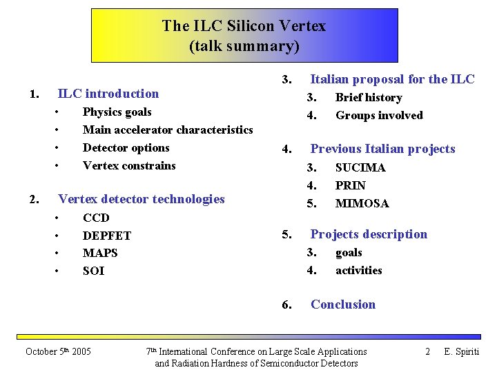
The ILC Silicon Vertex (talk summary) 1. ILC introduction • • 2. Physics goals Main accelerator characteristics Detector options Vertex constrains 3. 4. 4. CCD DEPFET MAPS SOI 5. October 5 th 2005 SUCIMA PRIN MIMOSA Projects description 3. 4. 6. Brief history Groups involved Previous Italian projects 3. 4. 5. Vertex detector technologies • • Italian proposal for the ILC goals activities Conclusion 7 th International Conference on Large Scale Applications and Radiation Hardness of Semiconductor Detectors 2 E. Spiriti

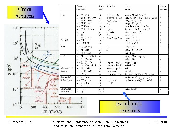
Cross sections Benchmark reactions October 5 th 2005 7 th International Conference on Large Scale Applications and Radiation Hardness of Semiconductor Detectors 3 E. Spiriti

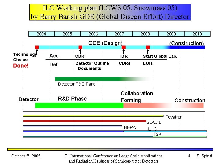
ILC Working plan (LCWS 05, Snowmass 05) by Barry Barish GDE (Global Disegn Effort) Director 2004 2005 2006 2007 2008 GDE (Design) Technology Choice Done! 2009 2010 (Construction) Acc. CDR TDR Start Global Lab. Detector Outline Documents CDRs LOIs Detector R&D Panel Detector R&D Phase Collaboration Forming Construction Tevatron SLAC B HERA October 5 th 2005 LHC T 2 K 7 th International Conference on Large Scale Applications and Radiation Hardness of Semiconductor Detectors 4 E. Spiriti

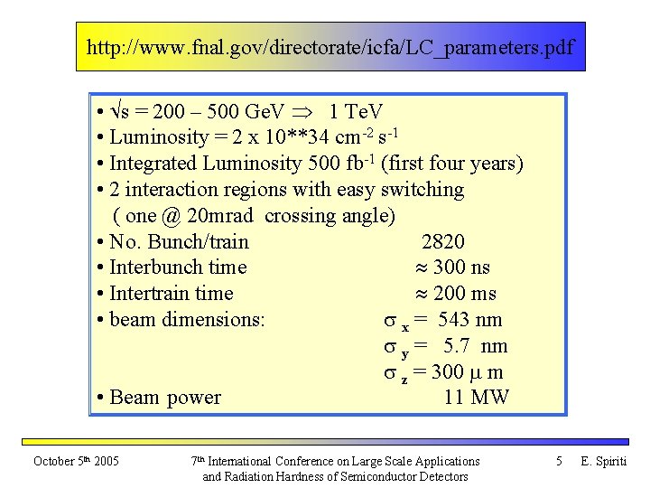
http: //www. fnal. gov/directorate/icfa/LC_parameters. pdf • s = 200 – 500 Ge. V 1 Te. V • Luminosity = 2 x 10**34 cm-2 s-1 • Integrated Luminosity 500 fb-1 (first four years) • 2 interaction regions with easy switching ( one @ 20 mrad crossing angle) • No. Bunch/train 2820 • Interbunch time 300 ns • Intertrain time 200 ms • beam dimensions: x = 543 nm y = 5. 7 nm z = 300 m • Beam power 11 MW October 5 th 2005 7 th International Conference on Large Scale Applications and Radiation Hardness of Semiconductor Detectors 5 E. Spiriti

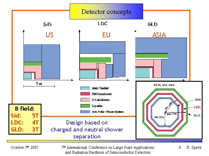
Detector concepts US B field: Sid: 5 T LDC: 4 T GLD: 3 T October 5 th 2005 EU ASIA Design based on charged and neutral shower separation 7 th International Conference on Large Scale Applications and Radiation Hardness of Semiconductor Detectors 6 E. Spiriti

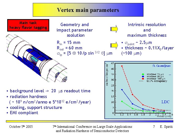
Vertex main parameters Main task heavy flavor tagging Geometry and impact parameter resolution Intrinsic resolution and maximum thickness Rin = 15 mm Rout = 60 mm ip = [5 10/p sin • point ~ 2. 5 m • thickness ~ 0. 1%X 0/layer (~100 m) 3/2 ] m • background level -> 20 s readout time • radiation hardness ( ~ 109 n/cm 2/anno e 5*1012 e/cm 2/year) • cooling, support structure • EMI compliant October 5 th 2005 7 th International Conference on Large Scale Applications and Radiation Hardness of Semiconductor Detectors 7 E. Spiriti

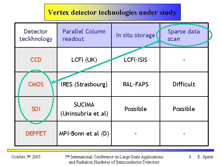
Vertex detector technologies under study Detector teckhnology Parallel Column readout In situ storage Sparse data scan CCD LCFI (UK) LCFI-ISIS - CMOS IRES (Strasbourg) RAL-FAPS Difficult SOI SUCIMA (Uninsubria et al) Possible DEPFET MPI-Bonn et al (D) - - October 5 th 2005 7 th International Conference on Large Scale Applications and Radiation Hardness of Semiconductor Detectors 8 E. Spiriti

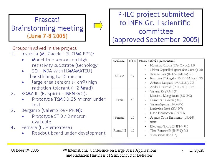
Frascati Brainstorming meeting (June 7 -8 2005) P-ILC project submitted to INFN Gr. I scientific committee (approved September 2005) Groups involved in the project 1. Insubria (M. Caccia - SUCIMA FP 5): • Monolithic sensors on high resistivity substrate (tecnology • SOI – NDA with HAMAMATSU) backthinnig to 15 micron • large area sensors (~ cm 2) high radiation tolerant (~ 2 Mrad) 2. ROMA III (E. Spiriti – INFN Gr 5): • Prototype TSMC 0. 25 micron under test 3. Bergamo (Valerio Re – PRIN): • Prototype ST 0. 13 micron available 4. Ferrara (L. Piemontese) • Readout board under development October 5 th 2005 7 th International Conference on Large Scale Applications and Radiation Hardness of Semiconductor Detectors 9 E. Spiriti

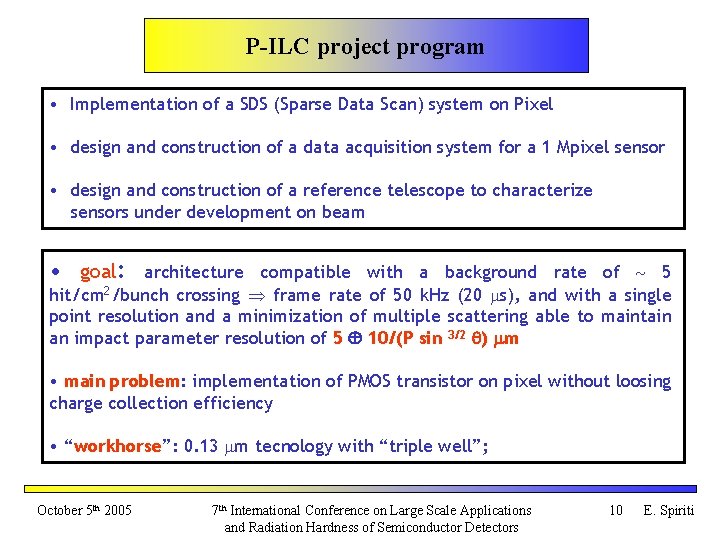
P-ILC project program • Implementation of a SDS (Sparse Data Scan) system on Pixel • design and construction of a data acquisition system for a 1 Mpixel sensor • design and construction of a reference telescope to characterize sensors under development on beam • goal: architecture compatible with a background rate of ~ 5 hit/cm 2/bunch crossing frame rate of 50 k. Hz (20 s), and with a single point resolution and a minimization of multiple scattering able to maintain an impact parameter resolution of 5 10/(P sin 3/2 ) m • main problem: implementation of PMOS transistor on pixel without loosing charge collection efficiency • “workhorse”: 0. 13 m tecnology with “triple well”; October 5 th 2005 7 th International Conference on Large Scale Applications and Radiation Hardness of Semiconductor Detectors 10 E. Spiriti

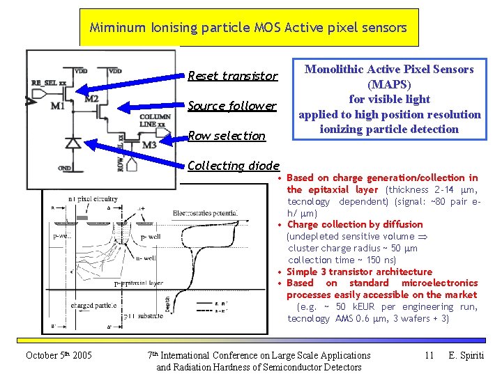
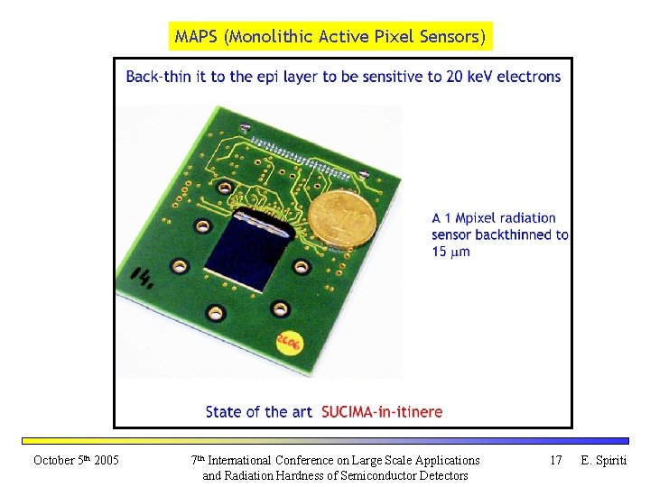
Miminum Ionising particle MOS Active pixel sensors Reset transistor Source follower Row selection Monolithic Active Pixel Sensors (MAPS) for visible light applied to high position resolution ionizing particle detection Collecting diode • Based on charge generation/collection in the epitaxial layer (thickness 2 -14 m, tecnology dependent) (signal: ~80 pair eh/ m) • Charge collection by diffusion (undepleted sensitive volume cluster charge radius ~ 50 m collection time ~ 150 ns) • Simple 3 transistor architecture • Based on standard microelectronics processes easily accessible on the market (e. g. ~ 50 k. EUR per engineering run, tecnology AMS 0. 6 m, 3 wafers + 3) October 5 th 2005 7 th International Conference on Large Scale Applications and Radiation Hardness of Semiconductor Detectors 11 E. Spiriti

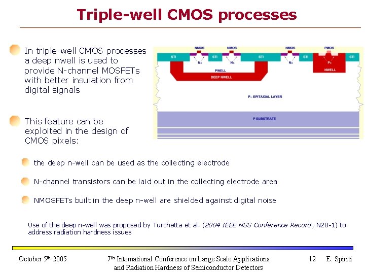
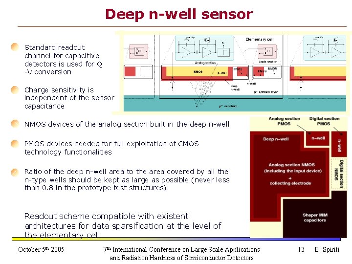
Triple-well CMOS processes In triple-well CMOS processes a deep nwell is used to provide N-channel MOSFETs with better insulation from digital signals This feature can be exploited in the design of CMOS pixels: the deep n-well can be used as the collecting electrode N-channel transistors can be laid out in the collecting electrode area NMOSFETs built in the deep n-well are shielded against digital noise Use of the deep n-well was proposed by Turchetta et al. (2004 IEEE NSS Conference Record, N 28 -1) to address radiation hardness issues October 5 th 2005 7 th International Conference on Large Scale Applications and Radiation Hardness of Semiconductor Detectors 12 E. Spiriti

Deep n-well sensor Standard readout channel for capacitive detectors is used for Q -V conversion Charge sensitivity is independent of the sensor capacitance NMOS devices of the analog section built in the deep n-well PMOS devices needed for full exploitation of CMOS technology functionalities Ratio of the deep n-well area to the area covered by all the n-type wells should be kept as large as possible (never less than 0. 8 in the prototype test structures) Readout scheme compatible with existent architectures for data sparsification at the level of the elementary cell October 5 th 2005 7 th International Conference on Large Scale Applications and Radiation Hardness of Semiconductor Detectors 13 E. Spiriti

A novel kind of CMOS MAPS has been designed and fabricated in a 0. 13 m CMOS technology Deep n-well is used as the sensitive electrode; a standard readout channel for capacitive detectors is employed to amplify the charge signal Tests with a laser source demonstrated that the sensor is capable of collecting and processing the charge Tests with radioactive sources are in progress Plans for the future: Optimization of the readout electronics and of the sensitive electrode layout (capacitance minimization) Design of a matrix with self trigger capability and sequential readout Submission of the same design in a different CMOS process (IBM, non epitaxial, triple well, 0. 13 m process, available through MOSIS, and/or CMOS process with optoelectronic features) October 5 th 2005 7 th International Conference on Large Scale Applications and Radiation Hardness of Semiconductor Detectors 14 E. Spiriti

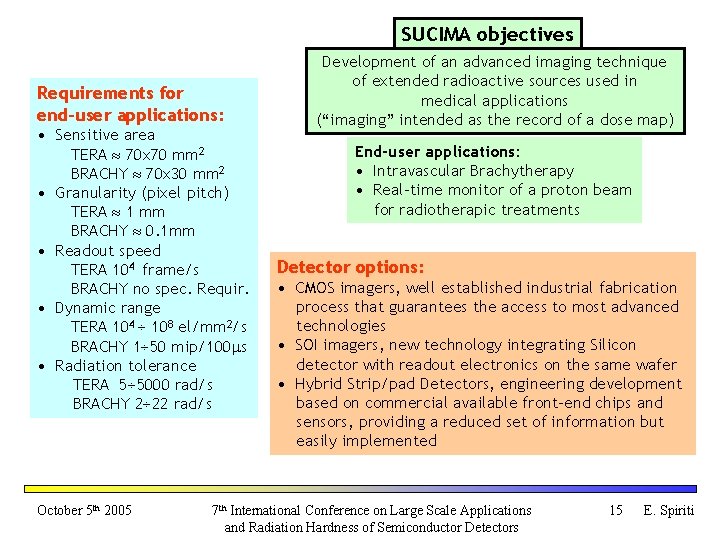
SUCIMA objectives Requirements for end-user applications: • Sensitive area TERA 70 x 70 mm 2 BRACHY 70 x 30 mm 2 • Granularity (pixel pitch) TERA 1 mm BRACHY 0. 1 mm • Readout speed TERA 104 frame/s BRACHY no spec. Requir. • Dynamic range TERA 104 108 el/mm 2/s BRACHY 1 50 mip/100 s • Radiation tolerance TERA 5 5000 rad/s BRACHY 2 22 rad/s October 5 th 2005 Development of an advanced imaging technique of extended radioactive sources used in medical applications (“imaging” intended as the record of a dose map) End-user applications: • Intravascular Brachytherapy • Real-time monitor of a proton beam for radiotherapic treatments Detector options: • CMOS imagers, well established industrial fabrication process that guarantees the access to most advanced technologies • SOI imagers, new technology integrating Silicon detector with readout electronics on the same wafer • Hybrid Strip/pad Detectors, engineering development based on commercial available front-end chips and sensors, providing a reduced set of information but easily implemented 7 th International Conference on Large Scale Applications and Radiation Hardness of Semiconductor Detectors 15 E. Spiriti

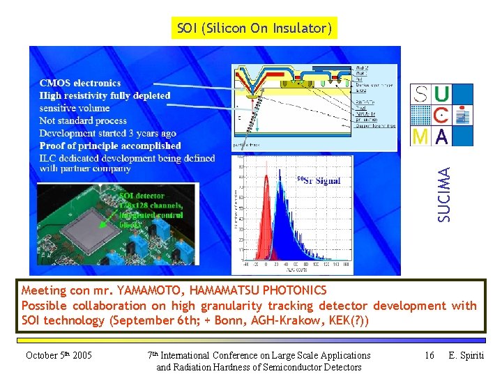
SUCIMA SOI (Silicon On Insulator) Meeting con mr. YAMAMOTO, HAMAMATSU PHOTONICS Possible collaboration on high granularity tracking detector development with SOI technology (September 6 th; + Bonn, AGH-Krakow, KEK(? )) October 5 th 2005 7 th International Conference on Large Scale Applications and Radiation Hardness of Semiconductor Detectors 16 E. Spiriti

MAPS (Monolithic Active Pixel Sensors) October 5 th 2005 7 th International Conference on Large Scale Applications and Radiation Hardness of Semiconductor Detectors 17 E. Spiriti

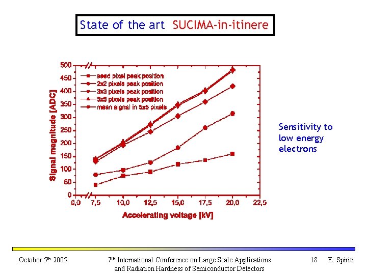
State of the art SUCIMA-in-itinere Sensitivity to low energy electrons October 5 th 2005 7 th International Conference on Large Scale Applications and Radiation Hardness of Semiconductor Detectors 18 E. Spiriti

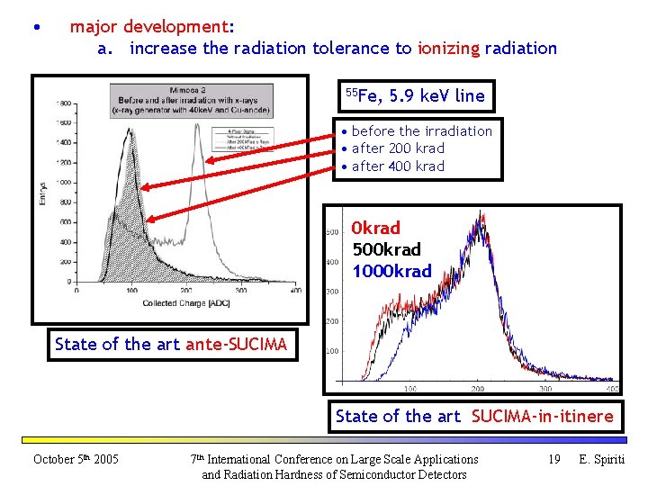
• major development: a. increase the radiation tolerance to ionizing radiation 55 Fe, 5. 9 ke. V line • before the irradiation • after 200 krad • after 400 krad 0 krad 500 krad 1000 krad State of the art ante-SUCIMA State of the art SUCIMA-in-itinere October 5 th 2005 7 th International Conference on Large Scale Applications and Radiation Hardness of Semiconductor Detectors 19 E. Spiriti

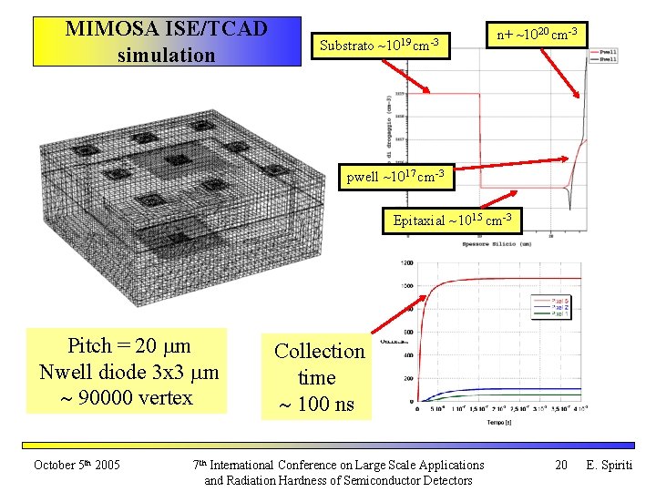
MIMOSA ISE/TCAD simulation Substrato ~1019 cm-3 n+ ~1020 cm-3 pwell ~1017 cm-3 Epitaxial ~1015 cm-3 Pitch = 20 m Nwell diode 3 x 3 m ~ 90000 vertex October 5 th 2005 Collection time ~ 100 ns 7 th International Conference on Large Scale Applications and Radiation Hardness of Semiconductor Detectors 20 E. Spiriti

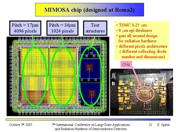
MIMOSA chip (designed at Roma 3) Pitch = 17 m 4096 pixels Pitch = 34 m 1024 pixels Test structures • TSMC 0. 25 m • 8 m epi thickness • gate all around design for radiation hardness • different pixels architecture ( different collecting diode number and dimensions) Chip October 5 th 2005 7 th International Conference on Large Scale Applications and Radiation Hardness of Semiconductor Detectors 21 E. Spiriti

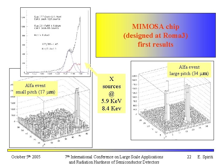
MIMOSA chip (designed at Roma 3) first results Alfa event small pitch (17 m) October 5 th 2005 X sources @ 5. 9 Ke. V 8. 4 Kev 7 th International Conference on Large Scale Applications and Radiation Hardness of Semiconductor Detectors Alfa event large pitch (34 m) 22 E. Spiriti

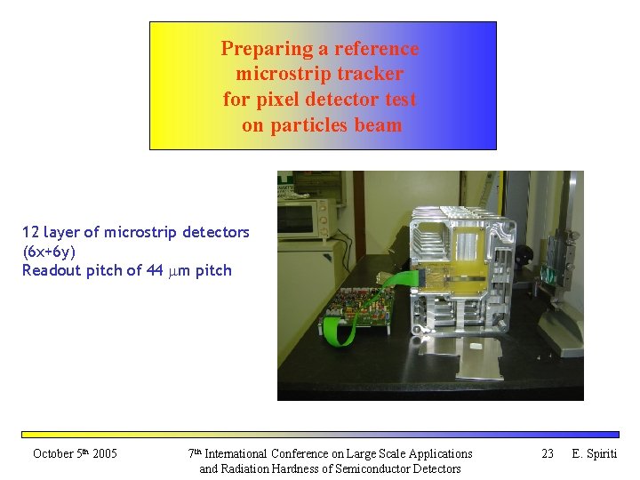
Preparing a reference microstrip tracker for pixel detector test on particles beam 12 layer of microstrip detectors (6 x+6 y) Readout pitch of 44 m pitch October 5 th 2005 7 th International Conference on Large Scale Applications and Radiation Hardness of Semiconductor Detectors 23 E. Spiriti

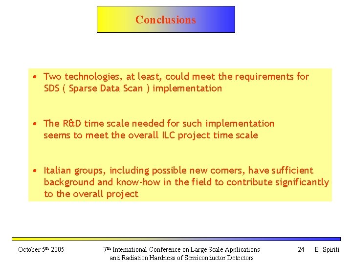
Conclusions • Two technologies, at least, could meet the requirements for SDS ( Sparse Data Scan ) implementation • The R&D time scale needed for such implementation seems to meet the overall ILC project time scale • Italian groups, including possible new comers, have sufficient background and know-how in the field to contribute significantly to the overall project October 5 th 2005 7 th International Conference on Large Scale Applications and Radiation Hardness of Semiconductor Detectors 24 E. Spiriti