HSTD8 Dec 2011 Academia Sinica Taiwan Development of

![Output of experimental vs simulation Voltage [m. V] Simulation Voltage [m. V] Experimental Time Output of experimental vs simulation Voltage [m. V] Simulation Voltage [m. V] Experimental Time](https://slidetodoc.com/presentation_image/62565ae63c4d4711a8b80d9267920d23/image-11.jpg)
![Energy spectra Isotope Counts ■ 22 Na ■ 137 Cs Energy [ke. V] MPPC Energy spectra Isotope Counts ■ 22 Na ■ 137 Cs Energy [ke. V] MPPC](https://slidetodoc.com/presentation_image/62565ae63c4d4711a8b80d9267920d23/image-12.jpg)
![Counts Coincidence timing spectrum 388 ps(FWHM) → ← Time [ns] • Coincidence of two Counts Coincidence timing spectrum 388 ps(FWHM) → ← Time [ns] • Coincidence of two](https://slidetodoc.com/presentation_image/62565ae63c4d4711a8b80d9267920d23/image-15.jpg)


- Slides: 32

HSTD-8 Dec 2011, Academia Sinica, Taiwan Development of an ultra-fast ASIC for future PET scanners using TOF-capable MPPC detectors Hidenori Matsuda (Waseda) J. Kataoka, T. Nakamori, T. Miura, T. kato (Waseda) H. Ikeda, G. Sato (JAXA) S. Nakamura, Y. Ishikawa, K. Sato, K. Yamamura, N. Kawabata (HPK. K. )

Overview Introduction - Previous work (APD-PET) - Motivation Development & performance of ASIC - Circuit architecture - Time measurement technique - Performance Summary & future prospect 2

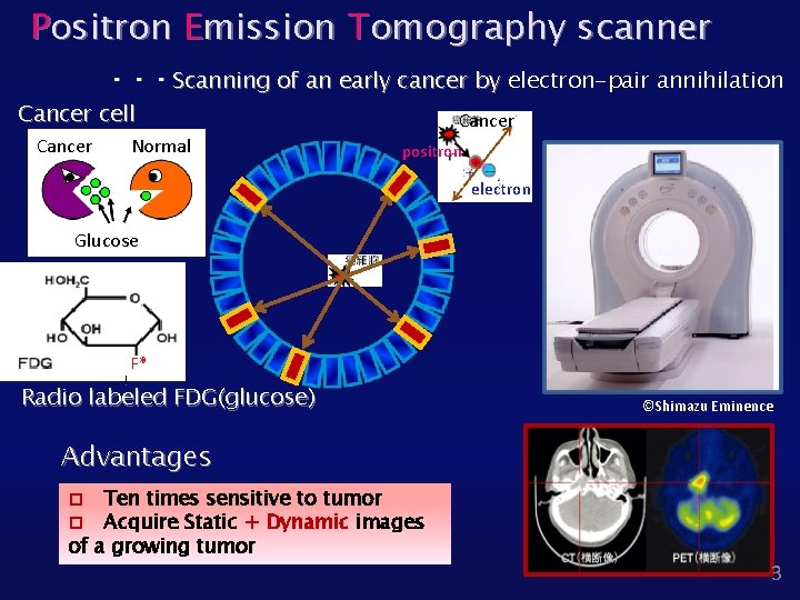
Positron Emission Tomography scanner ・・・Scanning of an early cancer by electron-pair annihilation Cancer cell Cancer Normal Cancer positron electron Glucose l F* Radio labeled FDG(glucose) ©Shimazu Eminence Advantages □ Ten times sensitive to tumor □ Acquire Static + Dynamic images of a growing tumor 3

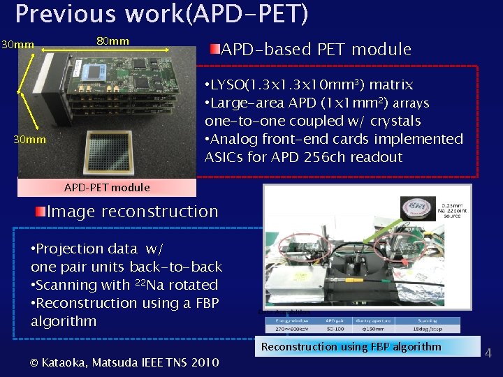
Previous work(APD-PET) 30 mm 80 mm APD-based PET module • LYSO(1. 3 x 10 mm 3) matrix • Large-area APD (1 x 1 mm 2) arrays one-to-one coupled w/ crystals • Analog front-end cards implemented ASICs for APD 256 ch readout 30 mm APD-PET module Image reconstruction • Projection data w/ one pair units back-to-back • Scanning with 22 Na rotated • Reconstruction using a FBP algorithm © Kataoka, Matsuda IEEE TNS 2010 Reconstruction using FBP algorithm 4

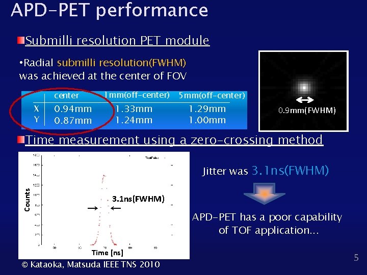
APD-PET performance Submilli resolution PET module • Radial submilli resolution(FWHM) was achieved at the center of FOV 1 mm(off-center) center X Y 0. 94 mm 0. 87 mm 1. 33 mm 1. 24 mm 5 mm(off-center) 1. 29 mm 1. 00 mm 0. 9 mm(FWHM) Time measurement using a zero-crossing method Counts Jitter was 3. 1 ns(FWHM) → ← Time [ns] © Kataoka, Matsuda IEEE TNS 2010 APD-PET has a poor capability of TOF application. . . 5

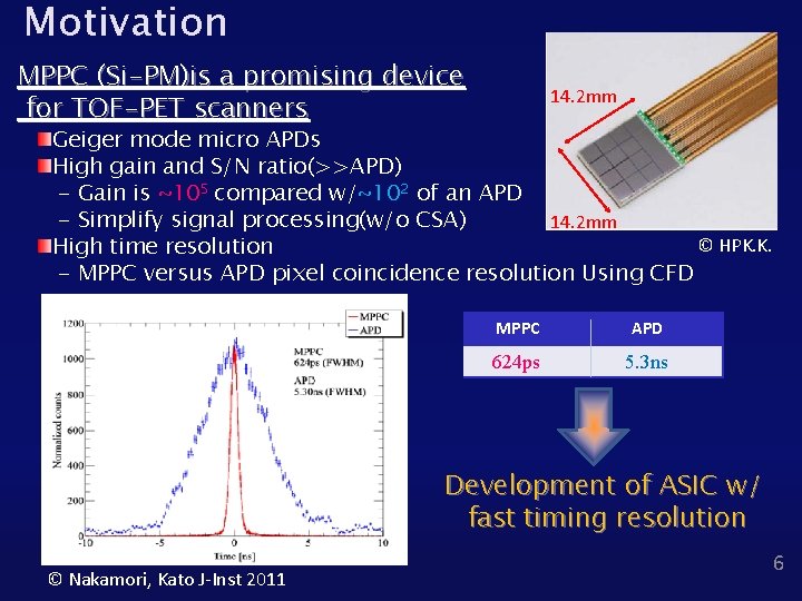
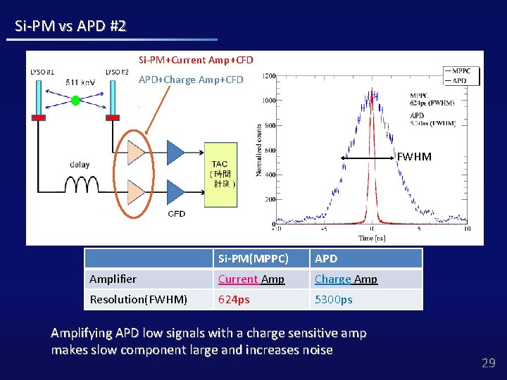
Motivation MPPC (Si-PM)is a promising device for TOF-PET scanners 14. 2 mm Geiger mode micro APDs High gain and S/N ratio(>>APD) - Gain is ~105 compared w/~102 of an APD - Simplify signal processing(w/o CSA) 14. 2 mm © HPK. K. High time resolution - MPPC versus APD pixel coincidence resolution Using CFD MPPC APD 624 ps 5. 3 ns Development of ASIC w/ fast timing resolution © Nakamori, Kato J-Inst 2011 6

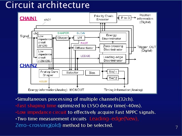
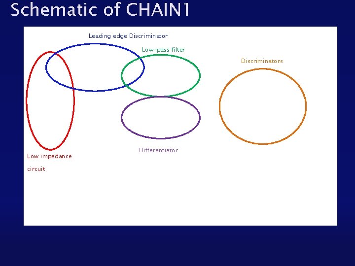
Circuit architecture CHAIN 1 CHAIN 2 • Simultaneous processing of multiple channels(32 ch). • Fast shaping time optimized to LYSO decay time(~40 ns). • Low impedance circuit to effectively acquire Fast MPPC signals. • Two time measurement circuits, Leading-edge(New), Zero-crossing(old) method to be selected. 7

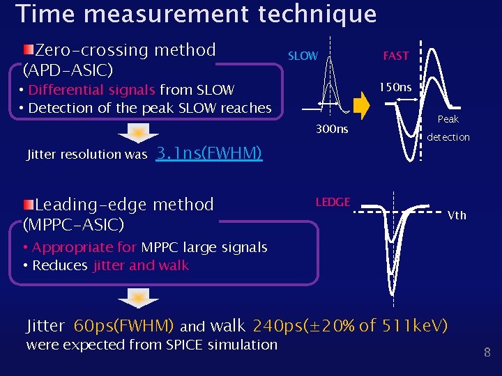
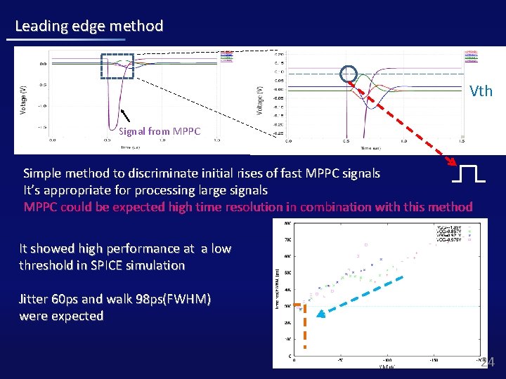
Time measurement technique Zero-crossing method (APD-ASIC) SLOW 150 ns • Differential signals from SLOW • Detection of the peak SLOW reaches 300 ns Jitter resolution was 3. 1 ns(FWHM) Leading-edge method (MPPC-ASIC) FAST LEDGE Peak detection Vth • Appropriate for MPPC large signals • Reduces jitter and walk Jitter 60 ps(FWHM) and walk 240 ps(± 20% of 511 ke. V) were expected from SPICE simulation 8

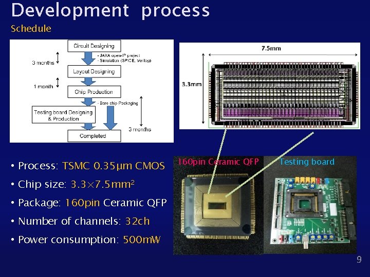
Development process Schedule • Process: TSMC 0. 35μm CMOS 160 pin Ceramic QFP Testing board • Chip size: 3. 3× 7. 5 mm 2 • Package: 160 pin Ceramic QFP • Number of channels: 32 ch • Power consumption: 500 m. W 9

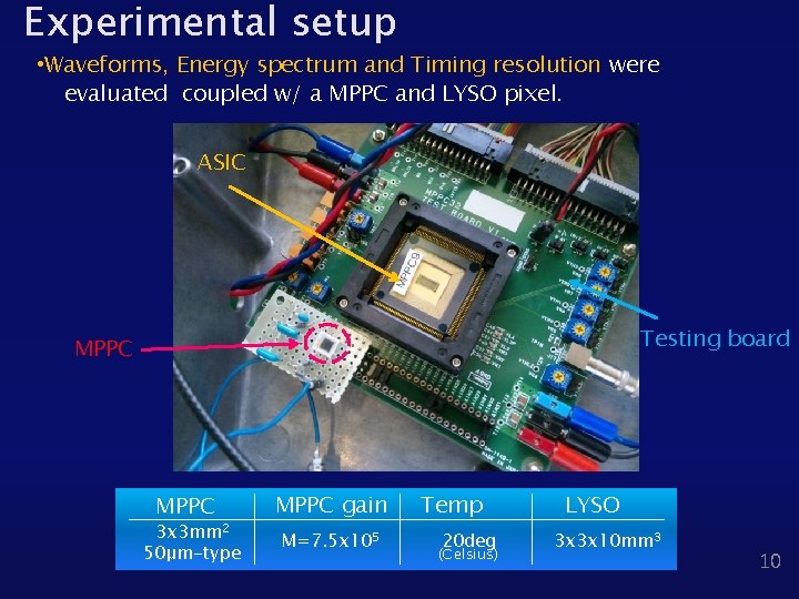
Experimental setup • Waveforms, Energy spectrum and Timing resolution were evaluated coupled w/ a MPPC and LYSO pixel. ASIC Testing board MPPC 3 x 3 mm 2 50μm-type MPPC gain M=7. 5 x 10⁵ Temp 20 deg (Celsius) LYSO 3 x 3 x 10 mm 3 10
![Output of experimental vs simulation Voltage m V Simulation Voltage m V Experimental Time Output of experimental vs simulation Voltage [m. V] Simulation Voltage [m. V] Experimental Time](https://slidetodoc.com/presentation_image/62565ae63c4d4711a8b80d9267920d23/image-11.jpg)
Output of experimental vs simulation Voltage [m. V] Simulation Voltage [m. V] Experimental Time [ns] ■LEDGE ■ASUM ■SHAPER ■SLOW ■FAST • Experimental waveforms were consistent w/ simulation results (MPPC signal input: 200 p. C, Gain=7. 5× 10⁵, 20 deg) • Gain dispersion and offset voltages were within adjustable ranges 11
![Energy spectra Isotope Counts 22 Na 137 Cs Energy ke V MPPC Energy spectra Isotope Counts ■ 22 Na ■ 137 Cs Energy [ke. V] MPPC](https://slidetodoc.com/presentation_image/62565ae63c4d4711a8b80d9267920d23/image-12.jpg)
Energy spectra Isotope Counts ■ 22 Na ■ 137 Cs Energy [ke. V] MPPC gain Energy resolution(FWHM) Cs 137 Na 22 9. 8% 10. 5% ・Excellent Resolution: 10. 5%(FWHM) @511 ke. V, 9. 8%(FWHM) @662 ke. V photopeak ⇒Nice performance for a PET device 12

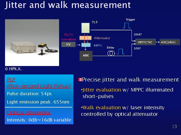
Jitter and walk measurement © HPK. K. PLP (Pico-second Light Pulsar) Pulse duration: 54 ps Light emission peak: 655 nm Optical attenuator Intensity: 0 d. B~ 16 d. B variable Precise jitter and walk measurement • Jitter evaluation w/ MPPC illuminated short-pulses • Walk evaluation w/ laser intensity controlled by optical attenuator 13

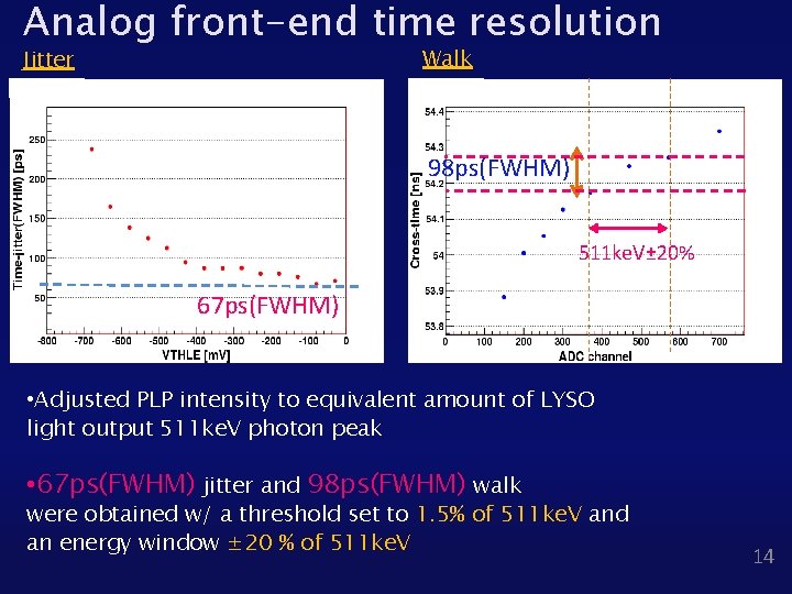
Analog front-end time resolution Walk Jitter 98 ps(FWHM) 511 ke. V± 20% 67 ps(FWHM) • Adjusted PLP intensity to equivalent amount of LYSO light output 511 ke. V photon peak • 67 ps(FWHM) jitter and 98 ps(FWHM) walk were obtained w/ a threshold set to 1. 5% of 511 ke. V and an energy window ± 20 % of 511 ke. V 14
![Counts Coincidence timing spectrum 388 psFWHM Time ns Coincidence of two Counts Coincidence timing spectrum 388 ps(FWHM) → ← Time [ns] • Coincidence of two](https://slidetodoc.com/presentation_image/62565ae63c4d4711a8b80d9267920d23/image-15.jpg)
Counts Coincidence timing spectrum 388 ps(FWHM) → ← Time [ns] • Coincidence of two MPPC modules and set a threshold at 1. 5% of 511 ke. V • Data collected at an energy window within ± 20% of 511 ke. V Coincidence time resolution 388 ps(FWHM) by simple leading-edge method 15

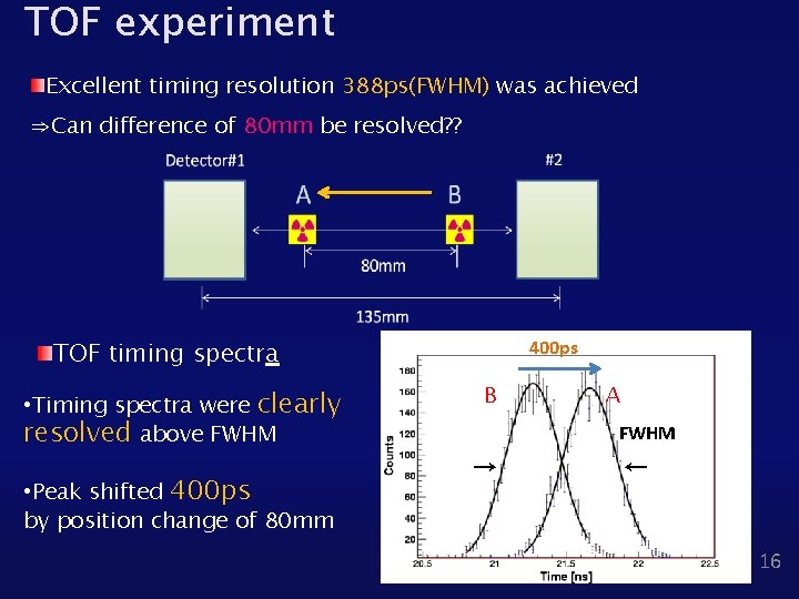
TOF experiment Excellent timing resolution 388 ps(FWHM) was achieved ⇒Can difference of 80 mm be resolved? ? 400 ps TOF timing spectra • Timing spectra were clearly resolved above FWHM • Peak shifted 400 ps by position change of 80 mm B → A FWHM ← 16

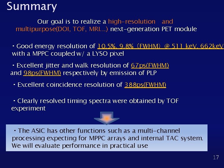
Summary Our goal is to realize a high-resolution and multipurpose(DOI, TOF, MRI. . . ) next-generation PET module ・Good energy resolution of 10. 5%, 9. 8%(FWHM)@ 511 ke. V, 662 ke. V with a MPPC coupled w/ a LYSO pixel ・Excellent jitter and walk resolution of 67 ps(FWHM) and 98 ps(FWHM) respectively by emission of PLP ・Excellent coincidence resolution of 388 ps(FWHM) ・Clearly resolved timing spectra were obtained by TOF experiment ・The ASIC has other functions such as a multi-channel processing expecting for MPPC arrays and internal TAC system. We will evaluate performance in practical use 17

THE END - Thank you!! -

APPENDIX

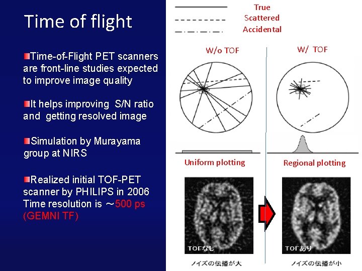
True Scattered Accidental Time of flight Time-of-Flight PET scanners are front-line studies expected to improve image quality W/o TOF W/ TOF It helps improving S/N ratio and getting resolved image Simulation by Murayama group at NIRS Realized initial TOF-PET scanner by PHILIPS in 2006 Time resolution is ~ 500 ps (GEMNI TF) Uniform plotting Regional plotting

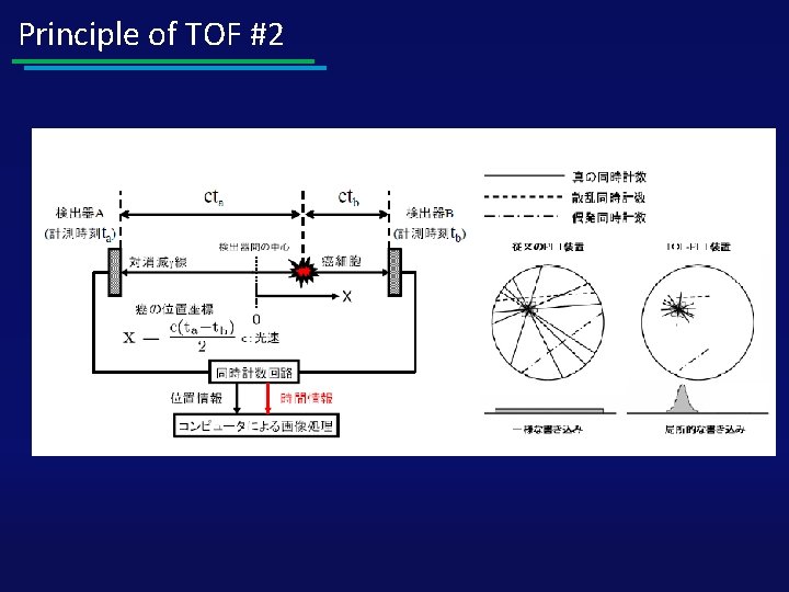
Principle of TOF #2

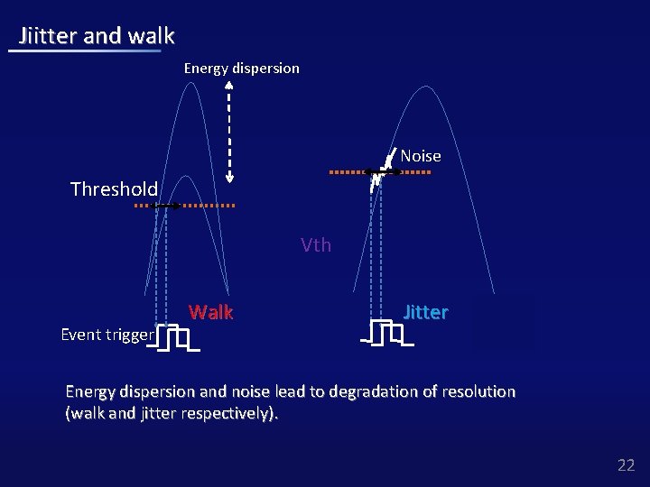
Jiitter and walk Energy dispersion Noise Threshold Vth Event trigger Walk Jitter Energy dispersion and noise lead to degradation of resolution (walk and jitter respectively). 22

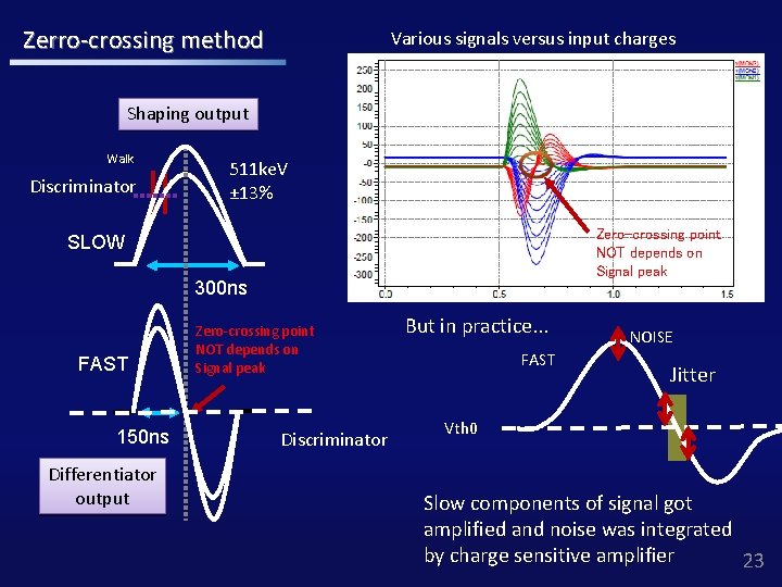
Zerro-crossing method Various signals versus input charges Shaping output Walk Discriminator 511 ke. V ± 13% Zero-crossing point NOT depends on Signal peak SLOW 300 ns FAST 150 ns Differentiator output Zero-crossing point NOT depends on Signal peak Discriminator But in practice. . . FAST NOISE Jitter Vth 0 Slow components of signal got amplified and noise was integrated by charge sensitive amplifier 23

Leading edge method Vth Signal from MPPC Simple method to discriminate initial rises of fast MPPC signals It’s appropriate for processing large signals MPPC could be expected high time resolution in combination with this method It showed high performance at a low threshold in SPICE simulation Jitter 60 ps and walk 98 ps(FWHM) were expected 24

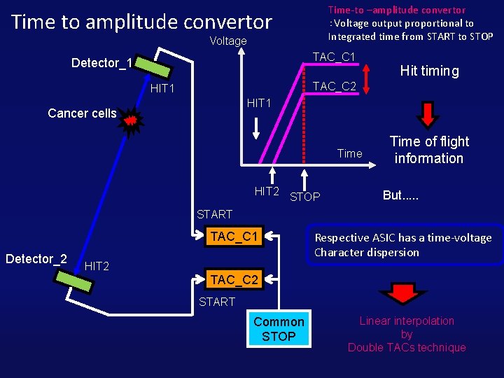
Time-to –amplitude convertor :Voltage output proportional to Integrated time from START to STOP Time to amplitude convertor Voltage TAC_C 1 Detector_1 Hit timing TAC_C 2 HIT 1 Cancer cells Time HIT 2 STOP Time of flight information But. . . START TAC_C 1 Detector_2 HIT 2 Respective ASIC has a time-voltage Character dispersion TAC_C 2 START Common STOP Linear interpolation by Double TACs technique

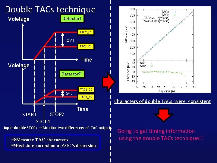
Double TACs technique Voletage Detector 1 TAC 2_C 1 ΔV 1 TAC 1_C 1 Time Voletage Detector2 TAC 2_C 2 ΔV 2 STOP 2 START STOP 1 TAC 1_C 2 Characters of double TACs were consistent Time Input double STOPs ⇒Monitor two differences of TAC outputs ⇒Measure TAC characters ⇒Real time correction of ASIC ‘s dispersion Going to get timing information using the double TACs technique!!

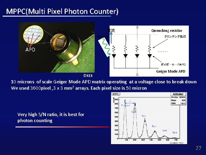
MPPC(Multi Pixel Photon Counter) 電流 Quenching resistor Photon APD ©KEK Geiger Mode APD 10 microns of scale Geiger Mode APD matrix operating at a voltage close to break down We used 3600 pixel , 3 x 3 mm 2 arrays. Each pixel size is 50 micron Very high S/N ratio, it is best for photon counting 27

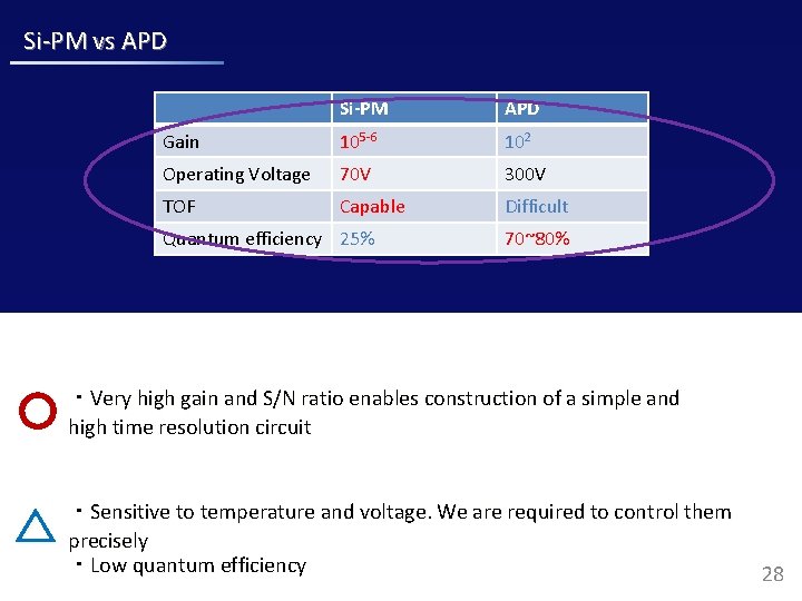
Si-PM vs APD Si-PM APD Gain 105 -6 102 Operating Voltage 70 V 300 V TOF Capable Difficult Quantum efficiency 25% 70~80% ・Very high gain and S/N ratio enables construction of a simple and high time resolution circuit △ ・Sensitive to temperature and voltage. We are required to control them precisely ・Low quantum efficiency 28

Si-PM vs APD #2 Si-PM+Current Amp+CFD APD+Charge Amp+CFD FWHM Si-PM(MPPC) APD Amplifier Current Amp Charge Amp Resolution(FWHM) 624 ps 5300 ps Amplifying APD low signals with a charge sensitive amp makes slow component large and increases noise 29

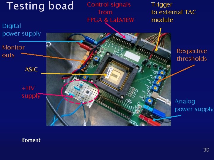
Testing boad Digital power supply Monitor outs Control signals from FPGA & Lab. VIEW Trigger to external TAC module Respective thresholds ASIC +HV supply Analog power supply Koment 30

Schematic of CHAIN 1 Leading edge Discriminator Low-pass filter Discriminators Low impedance circuit Differentiator

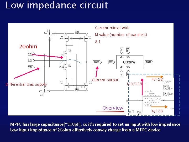
Low impedance circuit Current mirror with M value (number of parallels) 20 ohm Differential bias supply 8: 1 Current output Overview 120/128 4/128 MPPC has large capacitance(~300 p. F), so it’s required to set an input with low impedance Low Input impedance of 20 ohm effectively convey charge from a MPPC device