HPS CMS Si PM FrontEnd for HPS Sergey
- Slides: 6

HPS CMS Si. PM Front-End for HPS Sergey Los FNAL/CMS S. Los US HPS Workshop , September 27 -28, 2012 Fermilab 1

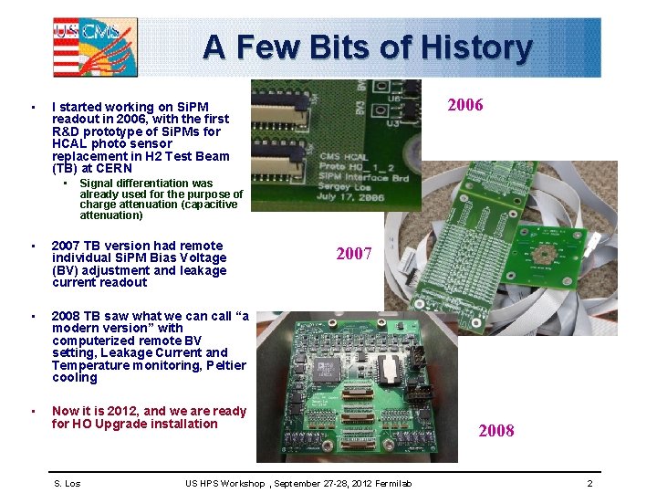
A Few Bits of History • 2006 I started working on Si. PM readout in 2006, with the first R&D prototype of Si. PMs for HCAL photo sensor replacement in H 2 Test Beam (TB) at CERN • Signal differentiation was already used for the purpose of charge attenuation (capacitive attenuation) • 2007 TB version had remote individual Si. PM Bias Voltage (BV) adjustment and leakage current readout • 2008 TB saw what we can call “a modern version” with computerized remote BV setting, Leakage Current and Temperature monitoring, Peltier cooling • Now it is 2012, and we are ready for HO Upgrade installation S. Los 2007 US HPS Workshop , September 27 -28, 2012 Fermilab 2008 2

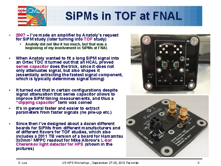
Si. PMs in TOF at FNAL • 2007 – I’ve made an amplifier by Anatoly’s request for Si. PM study (later turning into TOF study) • Anatoly did not like it too much, but that was a beginning of my involvement in Si. PMs at FNAL • When Anatoly wanted to fit a long Si. PM signal into an Ortec TDC it turned out that an HCAL proved series capacitor does the trick, since it does not only attenuates signal, but also shapes it (essentially extracting the fastest signal component, which is typically determines signal timing) • It turned out that in certain configurations despite signal attenuation that series capacitor allows to improve Si. PM timing measurements, and thus a “clipping capacitor” term was coined It’s in general faster and easier to extract parameters from faster signals (no pile-up etc. ) • • Since then I’ve designed about a dozen different boards for Si. PMs from different manufacturers and of different flavors for TOF studies, which also includes a 2011 TB version of a board for Hamamtsu 3 x 3 mm 2 MPPC readout for Mike Albrow’s L-bar Cherenkov light detector for HPS (shown in the pictures) S. Los US HPS Workshop , September 27 -28, 2012 Fermilab 3

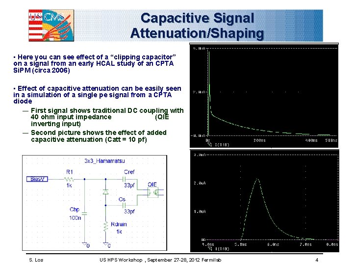
Capacitive Signal Attenuation/Shaping • Here you can see effect of a “clipping capacitor” on a signal from an early HCAL study of an CPTA Si. PM (circa 2006) • Effect of capacitive attenuation can be easily seen in a simulation of a single pe signal from a CPTA diode ― First signal shows traditional DC coupling with 40 ohm input impedance (QIE inverting input) ― Second picture shows the effect of added capacitive attenuation (Catt = 10 pf) S. Los US HPS Workshop , September 27 -28, 2012 Fermilab 4

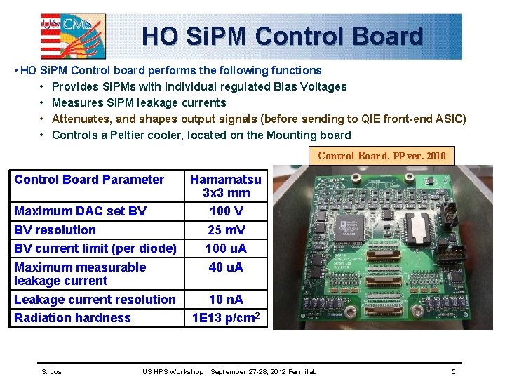
HO Si. PM Control Board • HO Si. PM Control board performs the following functions • Provides Si. PMs with individual regulated Bias Voltages • Measures Si. PM leakage currents • Attenuates, and shapes output signals (before sending to QIE front-end ASIC) • Controls a Peltier cooler, located on the Mounting board Control Board, PP ver. 2010 Control Board Parameter Maximum DAC set BV BV resolution BV current limit (per diode) Maximum measurable leakage current Leakage current resolution Radiation hardness S. Los Hamamatsu 3 x 3 mm 100 V 25 m. V 100 u. A 40 u. A 10 n. A 1 E 13 p/cm 2 US HPS Workshop , September 27 -28, 2012 Fermilab 5

HPS Si. PM Front-End Design • L-Bar Si. PM readout can be based on the 2011 TB version • Si. PM operations infrastructure can use HCAL Control board design • HCAL is I 2 C serial interface based, but can be adapted to virtually any interface • Preamplifiers with signal splitting will be integrated on the Si. PM mounting boards • Improves S/N performance • Splits signal for TOF/Trigger paths • Temperature monitoring for Si. PM gain control, no active cooling foreseen so far (might be needed to lower Si. PM noise rate if irradiation levels are high) • Hardware price is minimal, say $1000 per board (8 sets) • Most of the price is in engineering effort, my estimate is between 4 and 12 months over a 2 -year period, depending on how fancy we’d decide to go, and knowing more about operating conditions in the tunnel ($70 k-$200 k at Fermilab rates) S. Los US HPS Workshop , September 27 -28, 2012 Fermilab 6