How to use the VHDL and schematic design








- Slides: 19

How to use the VHDL and schematic design entry tools.

ABSTRACT Demonstrates how to create a top-level schematic that contains instantiations of the modules, and describe how to wire together the modules, and determine the circuit behavior by computer simulation.

Starting the Xilinx’s Software For PC users, start Xilinx program from the Start menu by selecting the following path: Start Programs Xilinx Foundation Series 2. 1 i Project Manager

Creating New Project Select OK New Project dialog box comes out Give “Name”—Lab 5; create the directory path —a: lab 5; Select OK

Creating a New Schematic Click on the third item named Schematic Editor in the first flow chart box. Schematic Editor

Schematic Editor Window Symbol Toolbox

Libraries Click on the Symbols Toolbox icon Click on Select Libraries

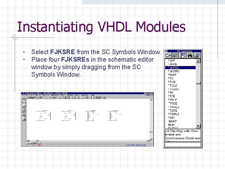
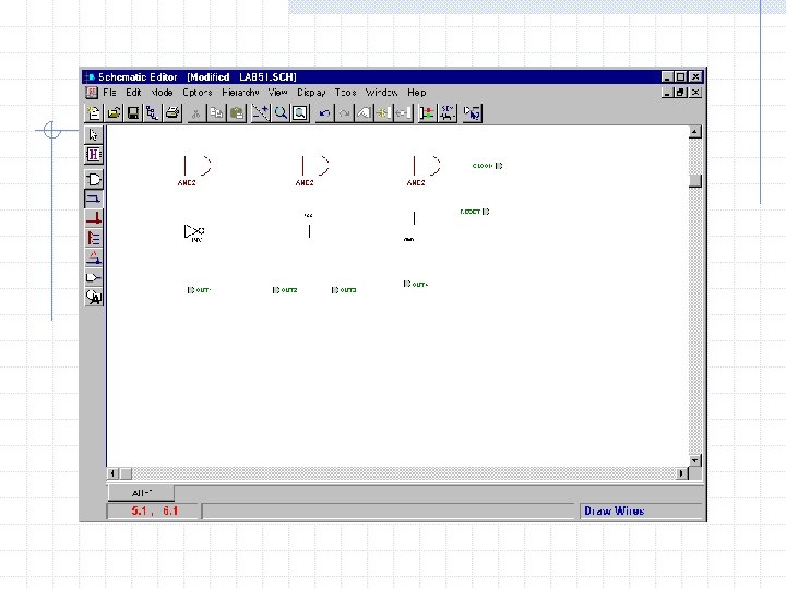
Instantiating VHDL Modules • Select FJKSRE from the SC Symbols Window. • Place four FJKSREs in the schematic editor window by simply dragging from the SC Symbols Window.

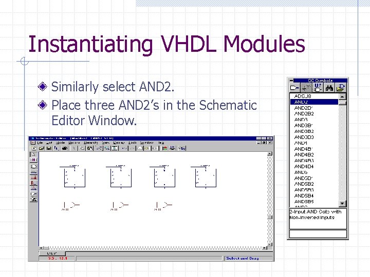
Instantiating VHDL Modules Similarly select AND 2. Place three AND 2’s in the Schematic Editor Window.

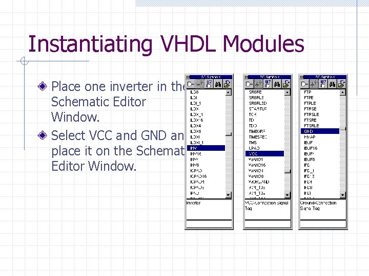
Instantiating VHDL Modules Place one inverter in the Schematic Editor Window. Select VCC and GND and place it on the Schematic Editor Window.

Adding Hierarchy Connectors Click on the Hierarchy Connector Symbol.


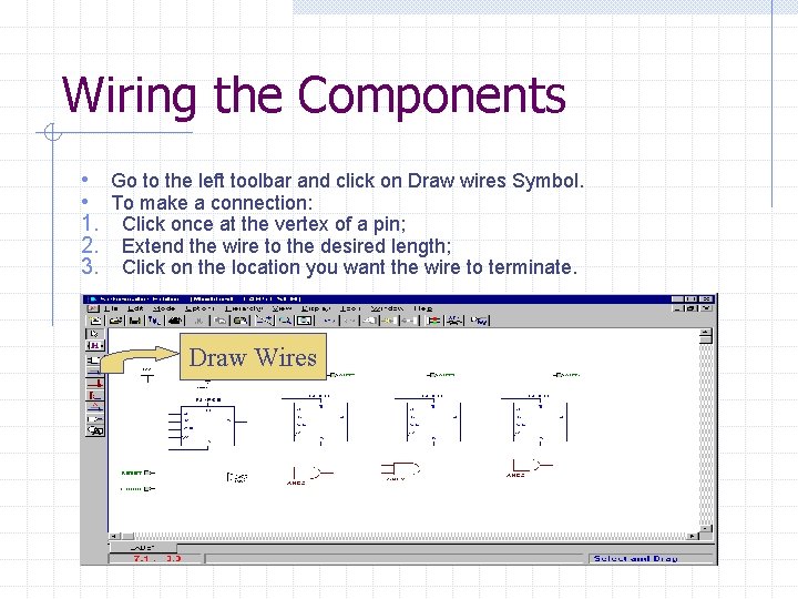
Wiring the Components • • 1. 2. 3. Go to the left toolbar and click on Draw wires Symbol. To make a connection: Click once at the vertex of a pin; Extend the wire to the desired length; Click on the location you want the wire to terminate. Draw Wires

Simulation Click on the Simulator button in the taskbar on the top of the workspace. Simulator

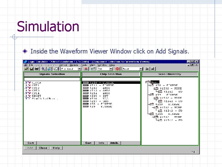
Simulation Inside the Waveform Viewer Window click on Add Signals. Double Click

Setting the Field Values Click on the text that says Clock, then click on the Select Simulator button in the Waveform Viewer Window. Select Double Simulators Click

Setting the Field Values Click on the text that says Reset, then click the Logic States Button. Simulation Step Logic States Click

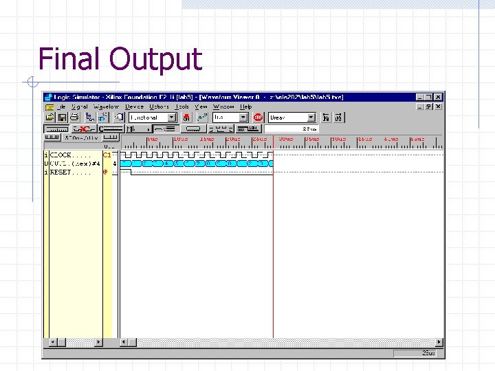
Final Output

Reference Lab Manual