How to use peripherals on MCB 1700 Vajih

How to use peripherals on MCB 1700 Vajih Montaghami Douglas W. Harder MTE 241 – Fall 2014
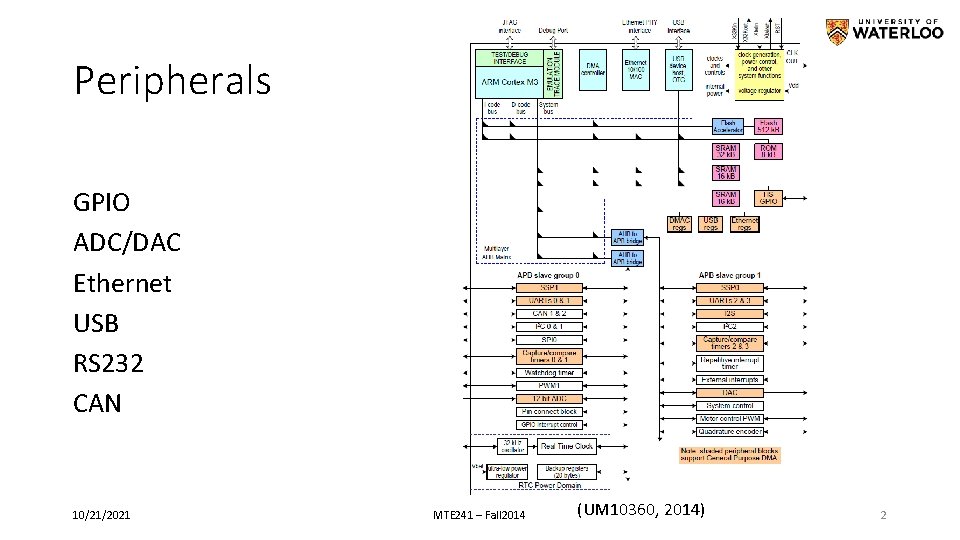
Peripherals GPIO ADC/DAC Ethernet USB RS 232 CAN 10/21/2021 MTE 241 – Fall 2014 (UM 10360, 2014) 2
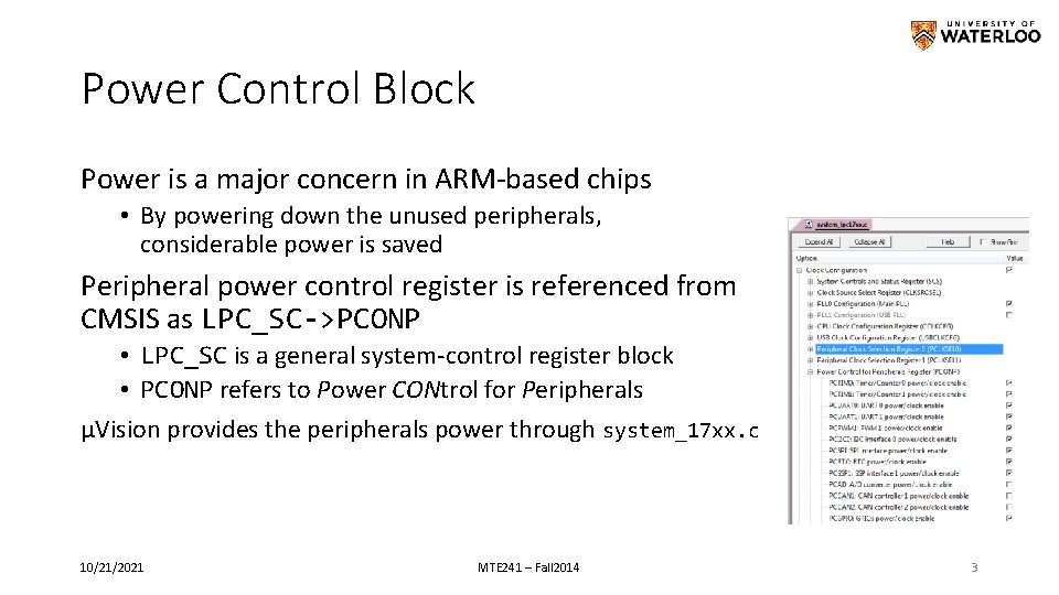
Power Control Block Power is a major concern in ARM-based chips • By powering down the unused peripherals, considerable power is saved Peripheral power control register is referenced from CMSIS as LPC_SC->PCONP • LPC_SC is a general system-control register block • PCONP refers to Power CONtrol for Peripherals µVision provides the peripherals power through system_17 xx. c 10/21/2021 MTE 241 – Fall 2014 3
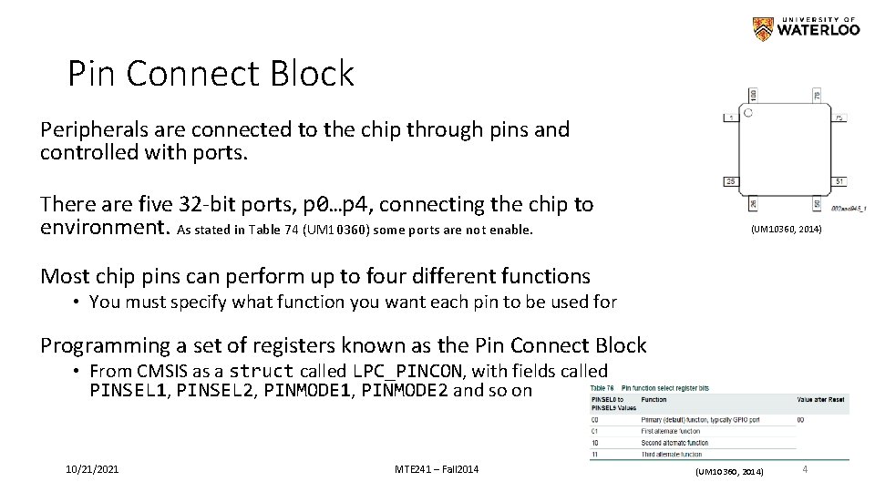
Pin Connect Block Peripherals are connected to the chip through pins and controlled with ports. There are five 32 -bit ports, p 0…p 4, connecting the chip to environment. As stated in Table 74 (UM 10360) some ports are not enable. (UM 10360, 2014) Most chip pins can perform up to four different functions • You must specify what function you want each pin to be used for Programming a set of registers known as the Pin Connect Block • From CMSIS as a struct called LPC_PINCON, with fields called PINSEL 1, PINSEL 2, PINMODE 1, PINMODE 2 and so on 10/21/2021 MTE 241 – Fall 2014 (UM 10360, 2014) 4
Interrupt Service Routine • Almost all peripherals can generate interrupts • The conditions on generating interrupts are different for each peripherals. • Interrupt Service Routines (ISR) in CMSIS is just a function with the interrupt source appended by _IRQHandler • E. g. ADC_IRQHandler • CMIS provides APIs for enabling/disabling, prioritizing, and Pending ISRs: void uint 32_t NVIC_Enable. IRQ( NVIC_Disable. IRQ( NVIC_Set. Priority( NVIC_Get. Priority( IRQn_Type IRQn ) IRQn, uint 32_t priority ) IRQn ) • Interrupts can be fired by setting an interrupt number to NVIC->STIR • But, they are cleared depending on the peripherals caused 10/21/2021 MTE 241 – Fall 2014 5
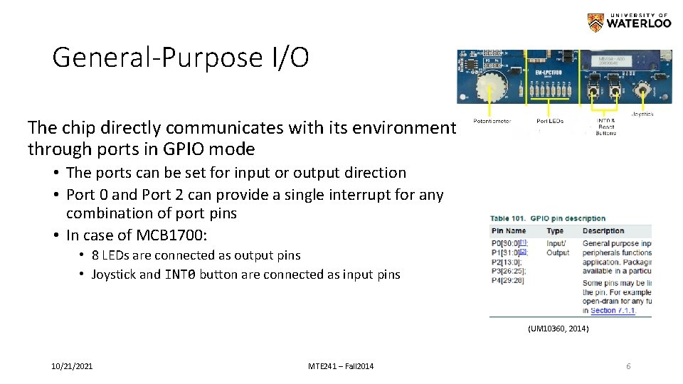
General-Purpose I/O The chip directly communicates with its environment through ports in GPIO mode • The ports can be set for input or output direction • Port 0 and Port 2 can provide a single interrupt for any combination of port pins • In case of MCB 1700: • 8 LEDs are connected as output pins • Joystick and INT 0 button are connected as input pins (UM 10360, 2014) 10/21/2021 MTE 241 – Fall 2014 6
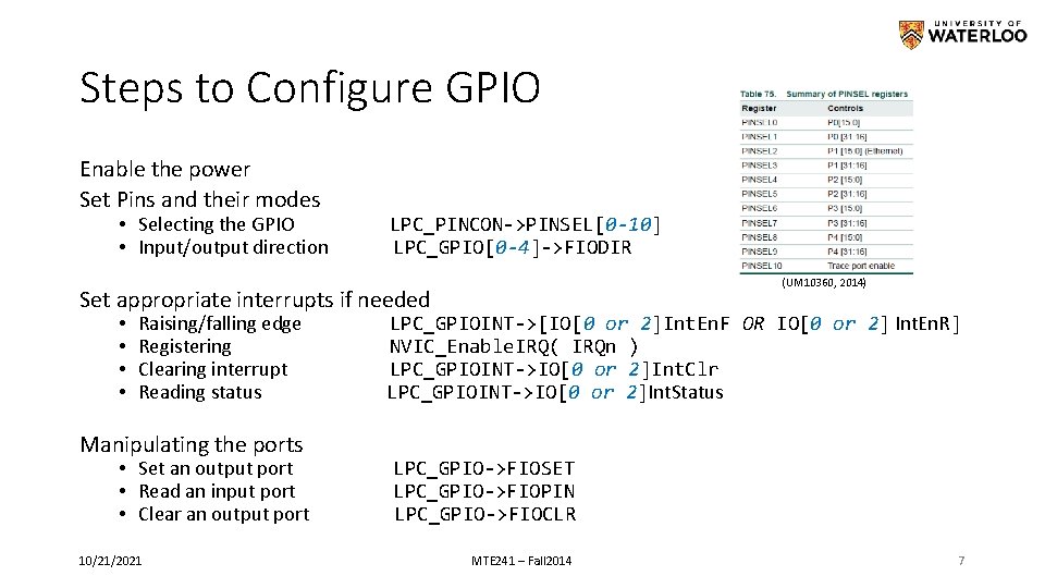
Steps to Configure GPIO Enable the power Set Pins and their modes • Selecting the GPIO • Input/output direction LPC_PINCON->PINSEL[0 -10] LPC_GPIO[0 -4]->FIODIR (UM 10360, 2014) Set appropriate interrupts if needed • • Raising/falling edge Registering Clearing interrupt Reading status Manipulating the ports • Set an output port • Read an input port • Clear an output port 10/21/2021 LPC_GPIOINT->[IO[0 or 2]Int. En. F OR IO[0 or 2] Int. En. R] NVIC_Enable. IRQ( IRQn ) LPC_GPIOINT->IO[0 or 2]Int. Clr LPC_GPIOINT->IO[0 or 2]Int. Status LPC_GPIO->FIOSET LPC_GPIO->FIOPIN LPC_GPIO->FIOCLR MTE 241 – Fall 2014 7
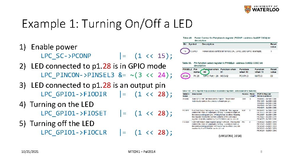
Example 1: Turning On/Off a LED 1) Enable power LPC_SC->PCONP |= (1 << 15); 2) LED connected to p 1. 28 is in GPIO mode LPC_PINCON->PINSEL 3 &= ~(3 << 24); 3) LED connected to p 1. 28 is an output pin LPC_GPIO 1 ->FIODIR 4) Turning on the LED LPC_GPIO 1 ->FIOSET 5) Turning off the LED LPC_GPIO 1 ->FIOCLR 10/21/2021 |= (1 << 28); MTE 241 – Fall 2014 (UM 10360, 2014) 8
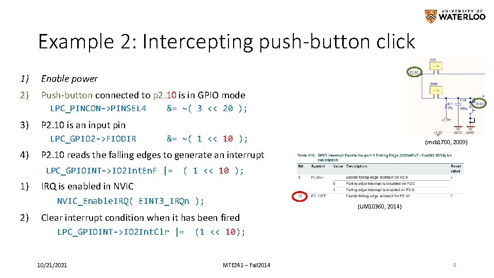
Example 2: Intercepting push-button click 1) Enable power 2) Push-button connected to p 2. 10 is in GPIO mode LPC_PINCON->PINSEL 4 3) P 2. 10 is an input pin LPC_GPIO 2 ->FIODIR 4) &= ~( 3 << 20 ); &= ~( 1 << 10 ); P 2. 10 reads the falling edges to generate an interrupt LPC_GPIOINT->IO 2 Int. En. F |= 1) ( 1 << 10 ); IRQ is enabled in NVIC_Enable. IRQ( EINT 3_IRQn ); 2) (mcb 1700, 2009) (UM 10360, 2014) Clear interrupt condition when it has been fired LPC_GPIOINT->IO 2 Int. Clr |= 10/21/2021 (1 << 10); MTE 241 – Fall 2014 9
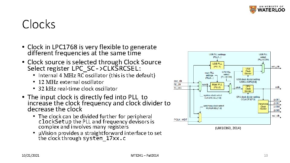
Clocks • Clock in LPC 1768 is very flexible to generate different frequencies at the same time • Clock source is selected through Clock Source Select register LPC_SC->CLKSRCSEL: • Internal 4 MHz RC oscillator (this is the default) • 12 MHz external oscillator • 32 k. Hz real-time clock oscillator • The input clock is directly fed into PLL to increase the clock frequency and clock divider to decrease the clock • The clock can be divided further for peripheral clock. Setup the PLL and frequency devisors is complex and involves many registers • µVision provides a straightforward interface to set the clock through system_17 xx. c 10/21/2021 MTE 241 – Fall 2014 (UM 10360, 2014) 10
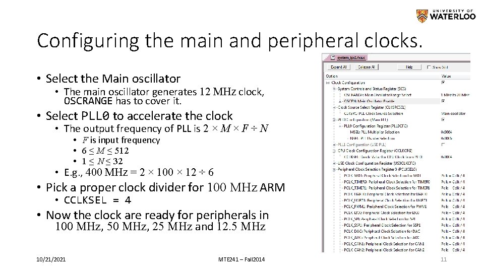
Configuring the main and peripheral clocks. • Select the Main oscillator • The main oscillator generates 12 MHz clock, OSCRANGE has to cover it. • Select PLL 0 to accelerate the clock • The output frequency of PLL is 2 × M × F ÷ N • F is input frequency • 6 ≤ M ≤ 512 • 1 ≤ N ≤ 32 • E. g. , 400 MHz = 2 × 100 × 12 ÷ 6 • Pick a proper clock divider for 100 MHz ARM • CCLKSEL = 4 • Now the clock are ready for peripherals in 100 MHz, 50 MHz, 25 MHz and 12. 5 MHz 10/21/2021 MTE 241 – Fall 2014 11
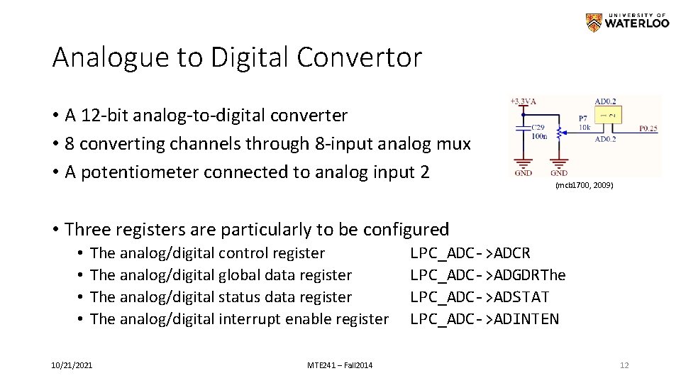
Analogue to Digital Convertor • A 12 -bit analog-to-digital converter • 8 converting channels through 8 -input analog mux • A potentiometer connected to analog input 2 (mcb 1700, 2009) • Three registers are particularly to be configured • • The analog/digital control register The analog/digital global data register The analog/digital status data register The analog/digital interrupt enable register 10/21/2021 MTE 241 – Fall 2014 LPC_ADC->ADCR LPC_ADC->ADGDRThe LPC_ADC->ADSTAT LPC_ADC->ADINTEN 12
ADC configuration steps • Set Power using PCONP register • Where is accessible in system_17 xx. c • Enable ADC 0 functionality pins through PINSEL registers • Set a Peripheral Clock using PCLKSEL 0 register • Already set through the IDE • Configure ADC through LPC_ADC->ADCR • Enable interrupts using CMSIS APIs • Now, start conversion. • Wait until the ADC status shows the conversion is done after ~52 ticks. • Response to the interrupt 10/21/2021 MTE 241 – Fall 2014 13
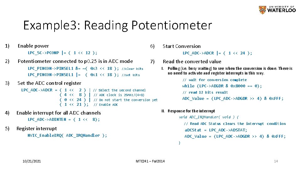
Example 3: Reading Potentiometer 1) Enable power 6) Start Conversion LPC_SC->PCONP |= ( 1 << 12 ); 2) LPC_ADC->ADCR |= ( 1 << 24 ); Potentiometer connected to p 0. 25 is in ADC mode LPC_PINCON->PINSEL 1 &= ~( 0 x 3 << 18 ); LPC_PINCON->PINSEL 1 |= ( 0 x 1 << 18 ); 3) 1 4 0 1 << 2 ) | << 8 ) | << 24 ) | << 21 ); //set bits I. Polling (i. e. busy waiting) to see when the conversion is done. There is no need to activate and register interrupts in this way. // wait for conversion complete // // while (LPC->ADGDR & 0 x 8000 == 0); Select the second channel ADC clock is 25 MHz/(4+1) Do not start the conversion yet Enable ADC Enable interrupt for all ADC channels LPC_ADC->ADINTEN = ( 1 << 5) //clear bits Read the converted value Set the ADC control register LPC_ADC->ADCR = ( ( 4) 7) // read 12 bits result ADC_Value = (LPC_ADC->ADGDR >> 4) & 0 x. FFF; II. Response for the interrupt void ADC_IRQHandler( void ) { 8); // Read ADC Status clears the interrupt condition Register interrupt a. DCStat = LPC_ADC->ADSTAT; ADC_Value = (LPC_ADC->ADGDR >> 4) & 0 x. FFF; NVIC_Enable. IRQ( ADC_IRQHandler ); } 10/21/2021 MTE 241 – Fall 2014 14
Resources Montaghami, V. I/O example: Cascading LEDs https: //ece. uwaterloo. ca/~dwharder/icsrts/Keil_board/IO_examples/src/io_example_project. zip LPC 176 x/5 x User manual. (1, April 2014). 3. 1, 846. NXP Semiconductor http: //www. nxp. com/documents/user_manual/UM 10360. pdf Roehl, B. (2011, April 18). Lab Manual for ECE 455. 39. Waterloo, ON, Canada http: //www. arm. com/files/pdf/ece 455 labmanual_preliminary. pdf Yiu, J. (2009). The Definitive Guide to the ARM® Cortex-M 3 MCB 1700 Schematic, (29, July 2009). 1. 2, 6, Keil. com http: //www. keil. com/mcb 1700 -schematics. pdf 10/21/2021 MTE 241 – Fall 2014 15
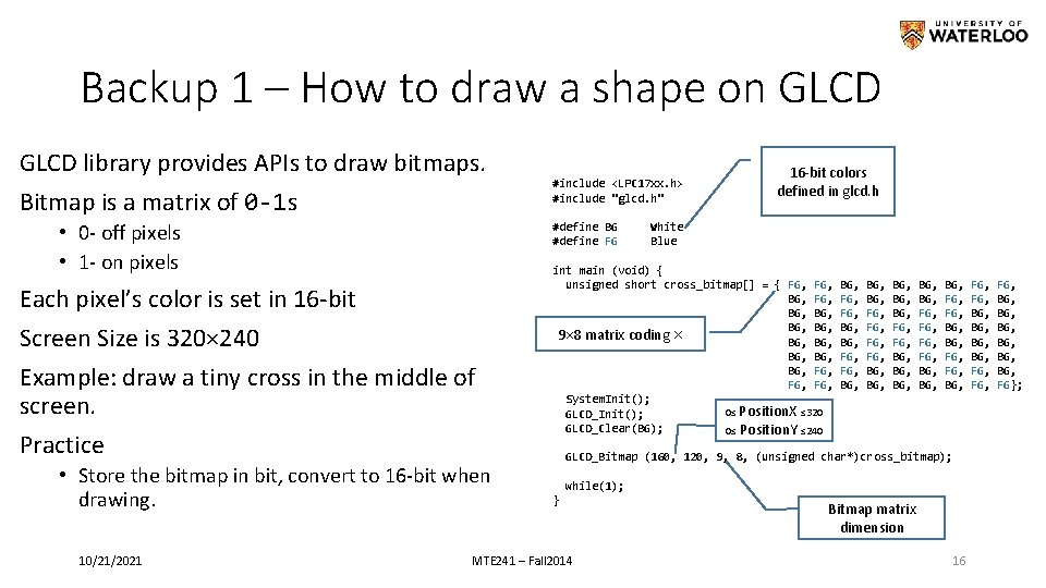
Backup 1 – How to draw a shape on GLCD library provides APIs to draw bitmaps. Bitmap is a matrix of 0 -1 s • 0 - off pixels • 1 - on pixels #define BG #define FG Each pixel’s color is set in 16 -bit Screen Size is 320× 240 Example: draw a tiny cross in the middle of screen. Practice • Store the bitmap in bit, convert to 16 -bit when drawing. 10/21/2021 #include <LPC 17 xx. h> #include "glcd. h" 16 -bit colors defined in glcd. h White Blue int main (void) { unsigned short cross_bitmap[] = { FG, BG, BG, 9× 8 matrix coding BG, BG, BG, FG, FG, System. Init(); 0≤ Position. X ≤ 320 GLCD_Init(); GLCD_Clear(BG); 0≤ Position. Y ≤ 240 × BG, FG, FG, BG, BG, BG, FG, BG, BG, BG, FG, FG, BG, GLCD_Bitmap (160, 120, 9, 8, (unsigned char*)cross_bitmap); while(1); } MTE 241 – Fall 2014 Bitmap matrix dimension 16 FG, BG, BG, FG, BG, BG, BG, FG};
- Slides: 16