Homogeneous Semiconductors Dopants Use Density of States and


 Energy Distribution Functions (Section 2. 9) Carrier Concentrations (Sections")
 can be found precisely if we know")

 conduction band EC S(E) EV valence band Ehole x")
 can be found precisely")
")
![f(E) = 1/{1+exp[(E-EF)/k. T]} 1 T=0 o. K T 1>0 T 2>T 1 f(E)](https://slidetodoc.com/presentation_image/2fb51c3615035eb279aac697e85f1ae1/image-14.jpg "f(E) = 1/{1+exp[(E-EF)/k. T]} 1 T=0 o. K T 1>0 T 2>T 1 f(E)")

![The Boltzmann Approximation If (E-EF)>k. T such that exp[(E-EF)/k. T] >> 1 then, f(E)](https://slidetodoc.com/presentation_image/2fb51c3615035eb279aac697e85f1ae1/image-16.jpg "The Boltzmann Approximation If (E-EF)>k. T such that exp[(E-EF)/k. T] >> 1 then, f(E)")
 f(E) 1 T=0 o. K T 1>0")
 fp(E) T=0 o. K 1 T 1>0")

 conduction band EC n(E) p(E) EF=Ei EV")
 conduction band EC n(E) p(E) EF EV")
 conduction band EC n(E) p(E) E EVF")


 For an intrinsic semiconductor, no=po and EF=Ei which gives")

 and ND ionized")

 1. The doping concentration")


![Summary non-degenerate: nopo= ni 2 degenerate n-type: nopo= ni 2 (ND/NC) exp[DEg*)/k. T] degenerate](https://slidetodoc.com/presentation_image/2fb51c3615035eb279aac697e85f1ae1/image-47.jpg "Summary non-degenerate: nopo= ni 2 degenerate n-type: nopo= ni 2 (ND/NC) exp[DEg*)/k. T] degenerate")
- Slides: 47
Homogeneous Semiconductors • Dopants • Use Density of States and Distribution Function to: • Find the Number of Holes and Electrons.
Energy Levels in Hydrogen Atom
Energy Levels for Electrons in a Doped Semiconductor
Assumptions for Calculation
Density of States (Appendix D) Energy Distribution Functions (Section 2. 9) Carrier Concentrations (Sections 2. 10 -12)
GOAL: • The density of electrons (no) can be found precisely if we know 1. the number of allowed energy states in a small energy range, d. E: S(E)d. E “the density of states” 2. the probability that a given energy state will be occupied by an electron: f(E) “the distribution function” no = S(E)f(E)d. E band
For quasi-free electrons in the conduction band: 1. We must use the effective mass (averaged over all directions) 2. the potential energy Ep is the edge of the conduction band (EC) For holes in the valence band: 1. We still use the effective mass (averaged over all directions) 2. the potential energy Ep is the edge of the valence band (EV)
Energy Band Diagram Eelectron E(x) conduction band EC S(E) EV valence band Ehole x note: increasing electron energy is ‘up’, but increasing hole energy is ‘down’.
Reminder of our GOAL: • The density of electrons (no) can be found precisely if we know 1. the number of allowed energy states in a small energy range, d. E: S(E)d. E “the density of states” 2. the probability that a given energy state will be occupied by an electron: f(E) “the distribution function” no = S(E)f(E)d. E band
Fermi-Dirac Distribution The probability that an electron occupies an energy level, E, is f(E) = 1/{1+exp[(E-EF)/k. T]} – where T is the temperature (Kelvin) – k is the Boltzmann constant (k=8. 62 x 10 -5 e. V/K) – EF is the Fermi Energy (in e. V) – (Can derive this – statistical mechanics. )
f(E) = 1/{1+exp[(E-EF)/k. T]} 1 T=0 o. K T 1>0 T 2>T 1 f(E) 0. 5 0 EF E All energy levels are filled with e-’s below the Fermi Energy at 0 o. K
Fermi-Dirac Distribution for holes Remember, a hole is an energy state that is NOT occupied by an electron. Therefore, the probability that a state is occupied by a hole is the probability that a state is NOT occupied by an electron: fp(E) = 1 – f(E) = 1 - 1/{1+exp[(E-EF)/k. T]} ={1+exp[(E-EF)/k. T]}/{1+exp[(E-EF)/k. T]} 1/{1+exp[(E-EF)/k. T]} = {exp[(E-EF)/k. T]}/{1+exp[(E-EF)/k. T]} =1/{exp[(EF - E)/k. T] + 1}
The Boltzmann Approximation If (E-EF)>k. T such that exp[(E-EF)/k. T] >> 1 then, f(E) = {1+exp[(E-EF)/k. T]}-1 {exp[(E-EF)/k. T]}-1 exp[-(E-EF)/k. T] …the Boltzmann approx. similarly, fp(E) is small when exp[(EF - E)/k. T]>>1: fp(E) = {1+exp[(EF - E)/k. T]}-1 {exp[(EF - E)/k. T]}-1 exp[-(EF - E)/k. T] If the Boltz. approx. is valid, we say the semiconductor is non-degenerate.
Putting the pieces together: for electrons, n(E) f(E) 1 T=0 o. K T 1>0 T 2>T 1 S(E) 0. 5 0 E EV EF EC n(E)=S(E)f(E) E
Putting the pieces together: for holes, p(E) fp(E) T=0 o. K 1 T 1>0 T 2>T 1 0. 5 S(E) 0 EV EF EC p(E)=S(E)f(E) hole energy E
Finding no and po the effective density of states in the conduction band
Energy Band Diagram intrinisic semiconductor: no=po=ni E(x) conduction band EC n(E) p(E) EF=Ei EV valence band x where Ei is the intrinsic Fermi level
Energy Band Diagram n-type semiconductor: no>po E(x) conduction band EC n(E) p(E) EF EV valence band x
Energy Band Diagram p-type semiconductor: po>no E(x) conduction band EC n(E) p(E) E EVF valence band x
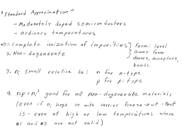
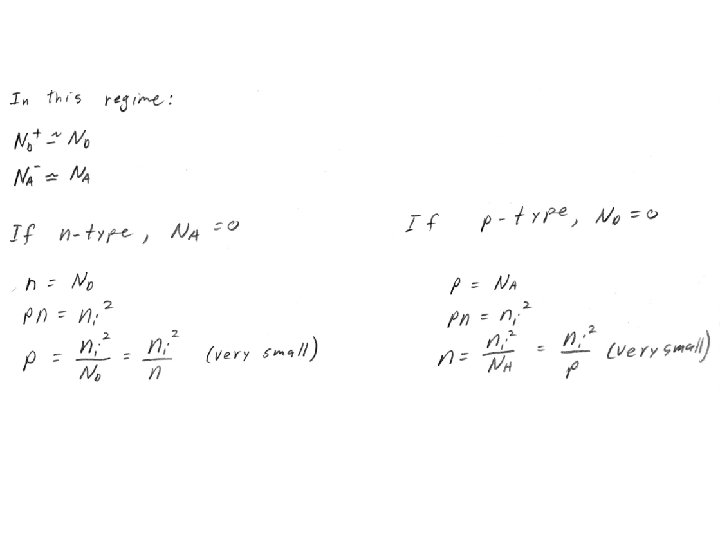
A very useful relationship …which is independent of the Fermi Energy Recall that ni = no= po for an intrinsic semiconductor, so nopo = ni 2 for all non-degenerate semiconductors. (that is as long as EF is not within a few k. T of the band edge)
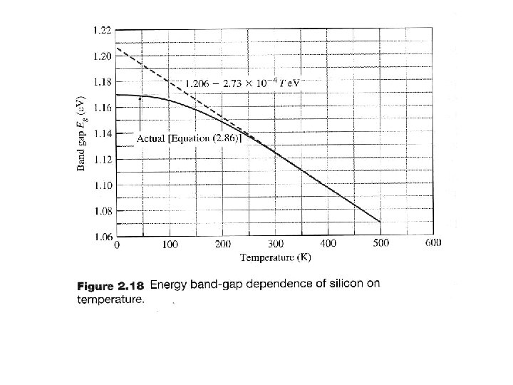
The intrinsic carrier density is sensitive to the energy bandgap, temperature, and m*
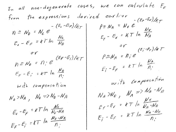
The intrinsic Fermi Energy (Ei) For an intrinsic semiconductor, no=po and EF=Ei which gives Ei = (EC + EV)/2 + (k. T/2)ln(NV/NC) so the intrinsic Fermi level is approximately in the middle of the bandgap.
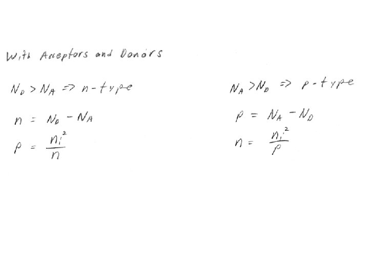
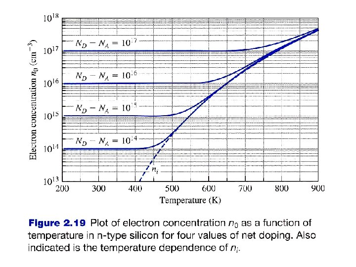
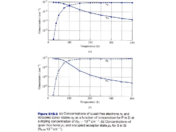
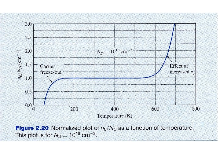
Higher Temperatures Consider a semiconductor doped with NA ionized acceptors (-q) and ND ionized donors (+q), do not assume that ni is small – high temperature expression. positive charges = negative charges po + ND = no + NA using ni 2 = nopo ni 2/no + ND = no+ NA ni 2 + no(ND-NA) - no 2 = 0 no = 0. 5(ND-NA) 0. 5[(ND-NA)2 + 4 ni 2]1/2 we use the ‘+’ solution since no should be increased by ni no = ND - NA in the limit that ni<<ND-NA
Temperature variation of some important “constants. ” Simpler Expression
Degenerate Semiconductors impurity band EC ED 1 + + Eg(ND) 1. The doping concentration is so high that EF moves within a few k. T of the band edge (EC or EV). Boltzman approximation not valid. 2. High donor concentrations cause the allowed donor wavefunctions to overlap, creating a band at Edn. First only the high states overlap, but eventually even the lowest state overlaps. Eg 0 This effectively decreases the bandgap by for ND > 1018 cm-3 in Si EV DEg = Eg 0 – Eg(ND).
Degenerate Semiconductors As the doping conc. increases more, EF rises above EC DEg available impurity band states filled impurity band states EC (intrinsic) EF EC (degenerate) ~ ED apparent band gap narrowing: DEg* (is optically measured) Eg* is the apparent band gap: - an electron must gain energy Eg* = EF-EV EV
Electron Concentration in degenerately doped n-type semiconductors The donors are fully ionized: no = ND The holes still follow the Boltz. approx. since EF-EV>>>k. T po = NV exp[-(EF-EV)/k. T] = NV exp[-(Eg*)/k. T] = NV exp[-(Ego- DEg*)/k. T] = NV exp[-Ego/k. T]exp[DEg*)/k. T] nopo = NDNVexp[-Ego/k. T] exp[DEg*)/k. T] = (ND/NC) NCNVexp[-Ego/k. T] exp[DEg*)/k. T] = (ND/NC)ni 2 exp[DEg*)/k. T]
Summary non-degenerate: nopo= ni 2 degenerate n-type: nopo= ni 2 (ND/NC) exp[DEg*)/k. T] degenerate p-type: nopo= ni 2 (NA/NV) exp[DEg*)/k. T]