History of Operating Systems Early batch system n

History of Operating Systems Early batch system n n bring cards to 1401 read cards to tape put tape on 7094 which does computing put tape on 1401 which prints output 1
 n John von Neumann invented von Neumann computer")
Long, Long Ago…(during the 1940 s) n John von Neumann invented von Neumann computer architecture n n n A CPU A memory unit I/O devices (e. g. , disks and tapes)

In von Neumann Architecture, n n n Programs are stored on storage devices Programs are copied into memory for execution CPU reads each instruction in the program and executes accordingly

A Simple CPU Model n n n Fetch-execute algorithm During a boot sequence, the program counter (PC) is loaded with the address of the first instruction The instruction register (IR) is loaded with the instruction from the address

Fetch-Execute Algorithm Simulation PC = <address of the first instruction> PC IR 3000 load r 3, b … load r 3, b 3000 load r 4, c 3004 … Memory addresses
 { // increment PC PC IR 3000 load r")
Fetch-Execute Algorithm while (not halt) { // increment PC PC IR 3000 load r 3, b … load r 3, b 3000 load r 4, c 3004 … Memory addresses
 { // increment PC PC 3004 // execute(IR) IR")
Fetch-Execute Algorithm while (not halt) { // increment PC PC 3004 // execute(IR) IR load r 3, b } // IR = memory // content of PC … load r 3, b 3000 load r 4, c 3004 … Memory addresses
 { // increment PC PC 3004 // execute(IR)")
Fetch-Execute Algorithm Simulation while (not halt) { // increment PC PC 3004 // execute(IR) IR load r 4, c } // IR = memory // content of PC … load r 3, b 3000 load r 4, c 3004 … Memory addresses

Communications devices Processing device Control unit Input devices Arithmetic/ logic unit Register storage area Memory Secondary storage Output devices

How the CPU Executes Program Instructions? n n Lets begin with one instruction only, to keep things simple Before an instruction can be executed, program instructions and data must be placed into the main memory from an input device or a secondary storage The data will probably make a temporary stop in a register Once the necessary data and instructions are in the memory, the CPU will perform the following four steps for each instruction:
 the")
The Four Steps. . . n n n 1. The CU fetches (gets) the instruction from the memory. 2. The CU decodes the instruction (decides what it means) and directs that necessary data be moved from memory to the ALU These first two steps together are called Instruction time or I-time.
… n 3. The ALU executes the arithmetic or logical instrucrtion.")
The Four Steps (contd)… n 3. The ALU executes the arithmetic or logical instrucrtion. n n n This means that the ALU is given control and it performs the actual operation on the data. 4. The ALU stores the result of this operation in memory or in a register (depending upon the requirement) Step 3 and 4 together are called Execution time or E-time. Schematic
 Decode (3) Execute I-time (1) Fetch E-time Registers")
Processing device Control unit ALU (2) Decode (3) Execute I-time (1) Fetch E-time Registers Memory (4) Store

And Then? n n n The CU eventually directs the memory to send the result to an output device (monitor etc. ) or a secondary storage device (HDD etc. ). The combination of I-time and E-time is called the machine cycle. Thus, n I-time + E-time = 1 -machine cycle

Some relevant facts… n n Each CPU has an internal clock that produces pulses at a fixed rate to synchronize all computer operations. A single machine instruction may be made up of a substantial number of sub-instructions, each of which must take at least 1 -clock cycle. Each type of CPU is designed to understand a specific group of instructions – such as ADD or MOVE – called the instruction set. Therefore, there are different instruction sets for different types of CPU’s.

Execution of an Instruction n Machine cycle n n Instruction phase n n n Instruction phase + Execution phase Step 1: Fetch instruction Step 2: Decode instruction Execute phase n n Step 3: Execute instruction Step 4: Store results

Data Storage n Short term storage n n n temp variables – e. g. , buffer containing the last key pressed program control data – e. g. , loop variables Long term storage n n Logging Data records Files
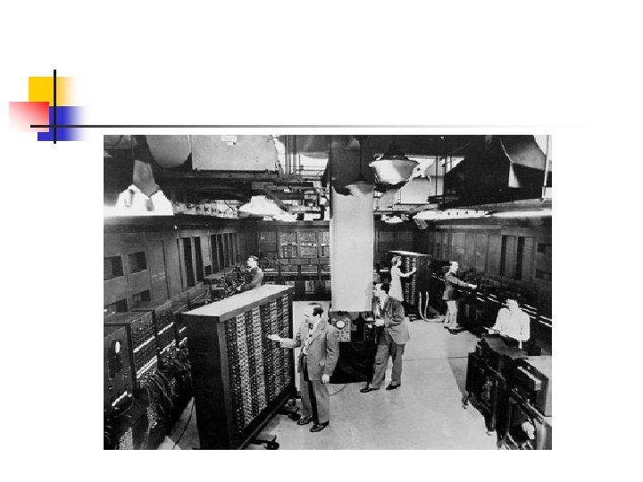
 Need: n n Army’s Ballistic Research Lab developed")
ENIAC (Electronic Numerical Integrator And Computer) Need: n n Army’s Ballistic Research Lab developed range and trajectory tables for new weapons Used >200 people with desktop calculators to create trajectory tables for weapons
 n n Mauchly (EE professor) and Eckert (grad student) at University of")
ENIAC (continued) n n Mauchly (EE professor) and Eckert (grad student) at University of Pennsylvania's Moore School of Electrical Engineering Proposed general purpose computer Started 1943 Finished 1946 n n 1 year to design 18 months to build Cost $500, 000 Too late for war effort
 General purpose nature proven by using ENIAC to perform calculations for: n")
ENIAC (continued) General purpose nature proven by using ENIAC to perform calculations for: n hydrogen bomb feasibility n weather prediction n cosmic-ray studies n thermal ignition n random-number studies n wind-tunnel design
 n n n Programmed manually by 6, 000 switches (programming took weeks)")
ENIAC (continued) n n n Programmed manually by 6, 000 switches (programming took weeks) Used 17, 468 vacuum tubes (relays had been used up to this point) Other components included 70, 000 resistors, 10, 000 capacitors, 1, 500 relays, and 5 million soldered joints 30 tons, 1800 square feet of floor space Consumed 160 kilowatts of electrical power
 n n n Twenty 10 digit accumulators Decimal (base-10) machine, each digit")
ENIAC (continued) n n n Twenty 10 digit accumulators Decimal (base-10) machine, each digit represented by one of ten tubes “ON” 5, 000 additions per second (1, 000 times faster then any other device at that time) 357 multiplications per second 38 divisions per second

ENIAC I/O n n n Constants were loaded using switches Numbers changed during the course of computation were entered using punch cards or punch tape The basic memory device was a flip-flip (latch) that had a neon lamp to represent its state

Dr. J. W. Mauchly makes an adjustment to ENIAC

http: //news. cnet. com/2009 -1006_3 -6037980. html

von Neumann/Turing Stored Program Computer n n ALU capable of operating on binary data Main memory stores both n n n instructions and data – must be considerable in order to carry out long, complicated sequences of operations Control Unit (CU) interprets instructions from memory and causes them to be executed Input and output equipment operated by control unit

von Neumann/Turing Stored Program Computer n n ALU capable of operating on binary data Both ALU & CU contain registers.
 n n n First implementation of von Neumann")
Princeton Institute for Advanced Studies (IAS) n n n First implementation of von Neumann stored program computer – the IAS computer Began in 1946 Completed in 1952

Structure of IAS machine

IAS Memory 1000 x 40 bit words of either number or instruction n Signed magnitude binary number n n n 1 sign bit 39 bits for magnitude 2 x 20 bit instructions n n n Left and right instructions (left executed first) 8 -bit opcode 12 bit address
 n n n n Memory")
IAS Registers n Set of registers (storage in CPU) n n n n Memory Buffer Register (MBR) Memory Address Register (MAR) Instruction Register (IR) Instruction Buffer Register (IBR) Program Counter (PC) Accumulator (AC) Multiplier Quotient (MQ)
: Contains a word to be")
IAS Registers n n n Memory buffer register (MBR): Contains a word to be stored in memory or sent to the I/O unit, or is used to receive a word from memory or from the I/O unit. Memory address register (MAR): Specifies the address in memory of the word to be written from or read into the MBR. Instruction register (IR): Contains the 8 -bit opcode instruction being executed.
: Employed to hold temporarily the")
IAS Registers n n n Instruction buffer register (IBR): Employed to hold temporarily the right-hand instruction from a word in memory. Program counter (PC): Contains the address of the next instruction-pair to be fetched from memory. Accumulator (AC) and multiplier quotient (MQ): Employed to hold temporarily operands and results of ALU operations. For example, the result of multiplying two 40 -bit numbers is an 80 -bit number; the most significant 40 bits are stored in the AC and the least significant in the MQ.

Structure of IAS Figure 2. 3, p. 22

Transistors n n n n Replaced vacuum tubes Smaller Cheaper Less heat dissipation Solid State device Made from Silicon (Sand) Invented 1947 at Bell Labs by William Shockley et al.

Moore’s Law n n n n n Gordon Moore - cofounder of Intel He observed (based on experience) that number of transistors on a chip doubled every year Since 1970’s growth has slowed a little Number of transistors doubles every 18 months Cost of a chip has remained almost unchanged Higher packing density means shorter electrical paths, giving higher performance Smaller size gives increased flexibility/portability Reduced power and cooling requirements Fewer system interconnections increases reliability

Growth in CPU Transistor Count

Effects of Moore’s Law The doubling of the number of transistors on a single chip every 18 months had some effects on the application of technology: n n n Costs have fallen dramatically since chip prices have not changed substantially since Moore made his prediction Tighter packaging has allowed for shorter electrical paths and therefore faster execution Smaller packaging has allowed for more applications in more environments Reduction in power and cooling requirements which also helps with portability Solder connections are not as reliable, therefore, with more functions on a single chip, there are fewer unreliable solder connections
 As technology allows for higher levels of performance, processor")
Effects of Moore’s Law (continued) As technology allows for higher levels of performance, processor designers must come up with ways to use it. n Keeping all parts of the processor busy n n Multiple processors Optimizing execution n Coordinating multiple pipelines Improved branch prediction Real-time analysis of code to “re-order” execution Speculative execution of code Incorporating multiple functions on single chip

Performance Mismatch n Experienced significant improvement n n n Processor speed Memory capacity Experienced only minor improvement n n n Memory speed Bus rates I/O device performance

Remember This? 42

Now Remember This Also! n Typical Memory Hierarchy n numbers shown are rough approximations 43

Memory Organization • In a typical computer system, the storage system is organized according to the following heirarchy: slow access (1 -5 s. ) and large capacity (almost unlimited) Archival Storage (magnetic tape or photographic) Moving head disk (magnetic or optical) High speed drum decreasing cost/bit Charge Coupled Device Main memory Cache Internal fast access (1 -20 ns. ) and small capacity (1 -4 K byte) decreasing access time
- Slides: 44