
HighPerformance System Design Prof Vojin G Oklobdzija September

High-Performance System Design Prof. Vojin G. Oklobdzija September 1, 2003 Prof. V. G. Oklobdzija: High. Performance System Design

Overview of the course Requirements: • Knowledge of CMOS digital circuits • Basic knowledge of analog circuits • Knowledge of Logic Design Textbook: • “High-Performance System Design: Circuits and Logic”, by V. G. Oklobdzija, IEEE Press 1999. • “Design of High-Performance Microprocessor Circuits”, by A. Chandrakasan, W. Bowhill, F. Fox, IEEE Press 2000. September 1, 2003 Prof. V. G. Oklobdzija: High-Performance System Design 2
Topics to be covered: I. Logic Design: A. Basic relations and analysis of CMOS B. Differential Logic – Issues II. High-performance sub-micron CMOS circuits. A. New Pass-Transistor Differential CMOS B. High-Speed and Low Power CMOS C. Examples from DPL and CPL. III. Low-Power Logic: IV. Timing and Clocking: V. Arithmetic Algorithms and Technology Mapping: September 1, 2003 Prof. V. G. Oklobdzija: High-Performance System Design 3

Grading • Quizzes & Take Home Exams……………. . 60% • Midterm Exam …………. . 40% • This may be adjusted after the second week of classes September 1, 2003 Prof. V. G. Oklobdzija: High-Performance System Design 4

Historical Overview • Invention of the transistor by Bardeen, Brattain and Shockley unveiled by Bell Laboratories on June 30, 1948. September 1, 2003 Prof. V. G. Oklobdzija: High-Performance System Design 5
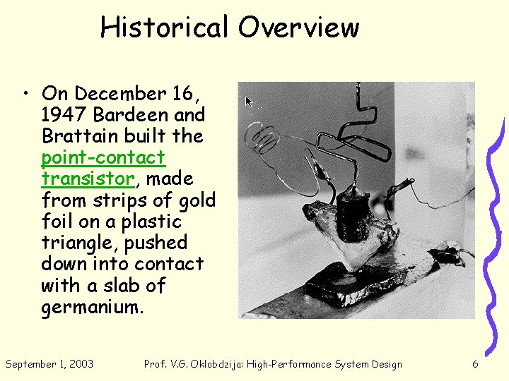
Historical Overview • On December 16, 1947 Bardeen and Brattain built the point-contact transistor, made from strips of gold foil on a plastic triangle, pushed down into contact with a slab of germanium. September 1, 2003 Prof. V. G. Oklobdzija: High-Performance System Design 6
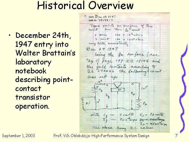
Historical Overview • December 24 th, 1947 entry into Walter Brattain’s laboratory notebook describing pointcontact transistor operation. September 1, 2003 Prof. V. G. Oklobdzija: High-Performance System Design 7
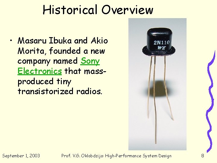
Historical Overview • Masaru Ibuka and Akio Morita, founded a new company named Sony Electronics that massproduced tiny transistorized radios. September 1, 2003 Prof. V. G. Oklobdzija: High-Performance System Design 8
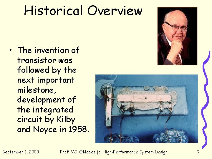
Historical Overview • The invention of transistor was followed by the next important milestone, development of the integrated circuit by Kilby and Noyce in 1958. September 1, 2003 Prof. V. G. Oklobdzija: High-Performance System Design 9
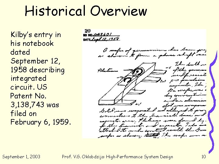
Historical Overview Kilby’s entry in his notebook dated September 12, 1958 describing integrated circuit. US Patent No. 3, 138, 743 was filed on February 6, 1959. September 1, 2003 Prof. V. G. Oklobdzija: High-Performance System Design 10
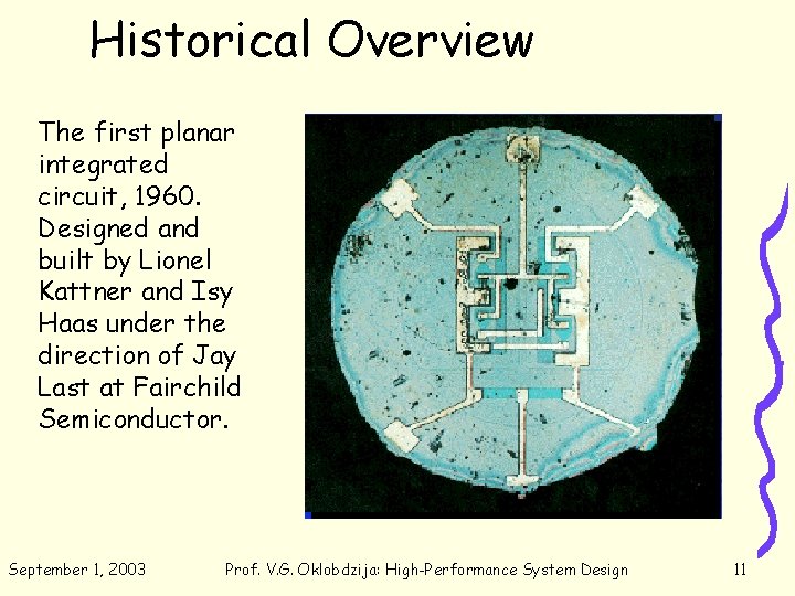
Historical Overview The first planar integrated circuit, 1960. Designed and built by Lionel Kattner and Isy Haas under the direction of Jay Last at Fairchild Semiconductor. September 1, 2003 Prof. V. G. Oklobdzija: High-Performance System Design 11
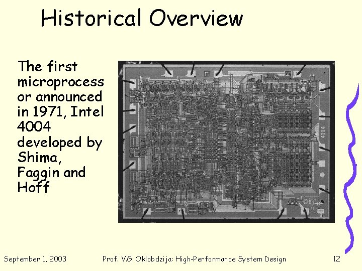
Historical Overview The first microprocess or announced in 1971, Intel 4004 developed by Shima, Faggin and Hoff September 1, 2003 Prof. V. G. Oklobdzija: High-Performance System Design 12
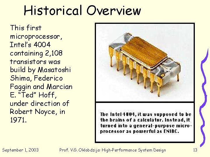
Historical Overview This first microprocessor, Intel’s 4004 containing 2, 108 transistors was build by Masatoshi Shima, Federico Faggin and Marcian E. “Ted” Hoff, under direction of Robert Noyce, in 1971. September 1, 2003 Prof. V. G. Oklobdzija: High-Performance System Design 13
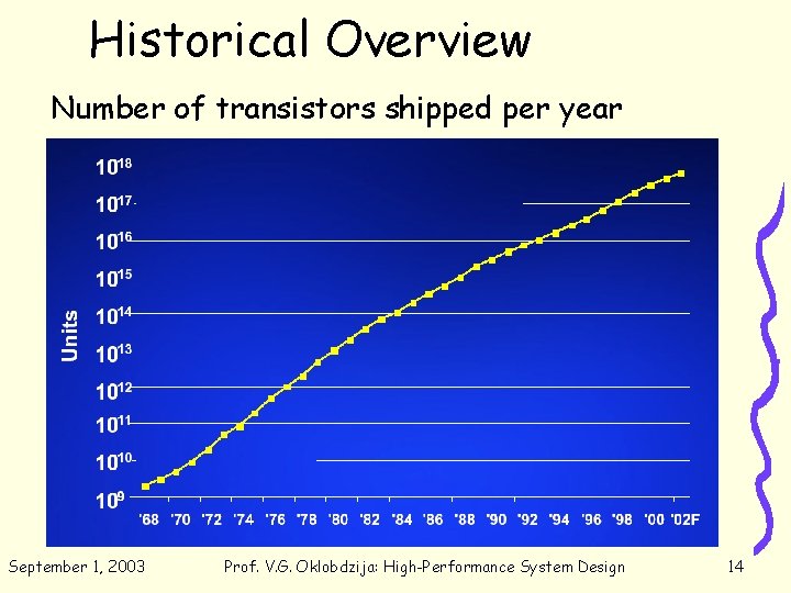
Historical Overview Number of transistors shipped per year September 1, 2003 Prof. V. G. Oklobdzija: High-Performance System Design 14

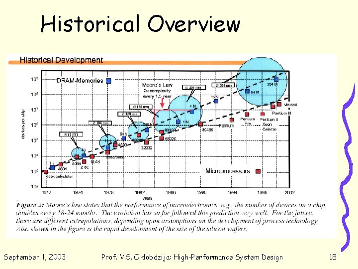
Historical Overview Moore’s law September 1, 2003 Prof. V. G. Oklobdzija: High-Performance System Design 15
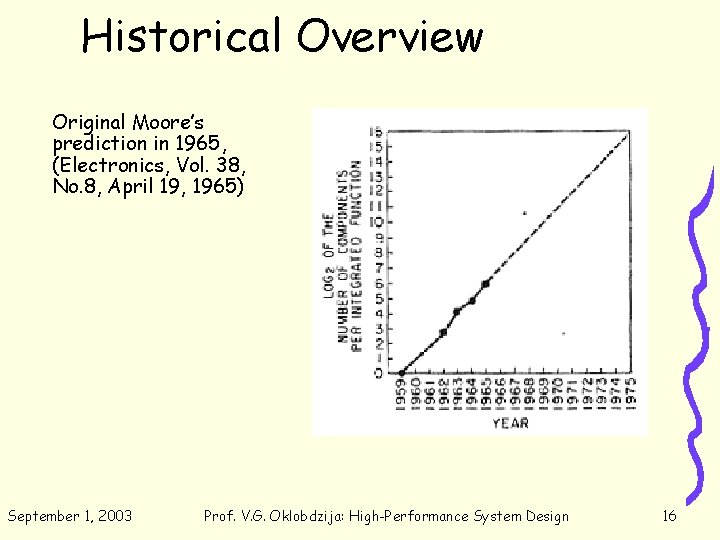
Historical Overview Original Moore’s prediction in 1965, (Electronics, Vol. 38, No. 8, April 19, 1965) September 1, 2003 Prof. V. G. Oklobdzija: High-Performance System Design 16
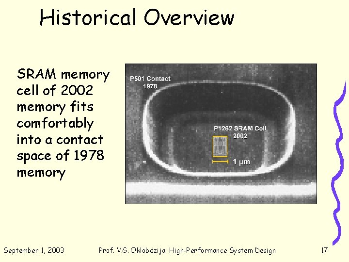
Historical Overview SRAM memory cell of 2002 memory fits comfortably into a contact space of 1978 memory September 1, 2003 Prof. V. G. Oklobdzija: High-Performance System Design 17
Historical Overview September 1, 2003 Prof. V. G. Oklobdzija: High-Performance System Design 18
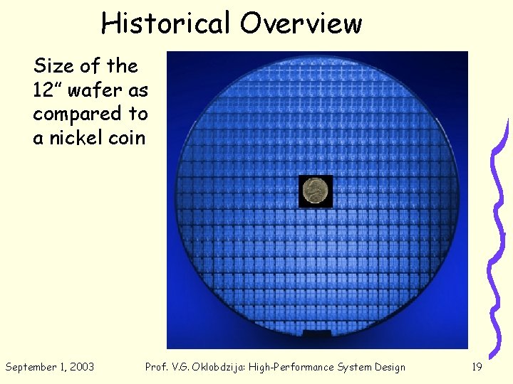
Historical Overview Size of the 12” wafer as compared to a nickel coin September 1, 2003 Prof. V. G. Oklobdzija: High-Performance System Design 19
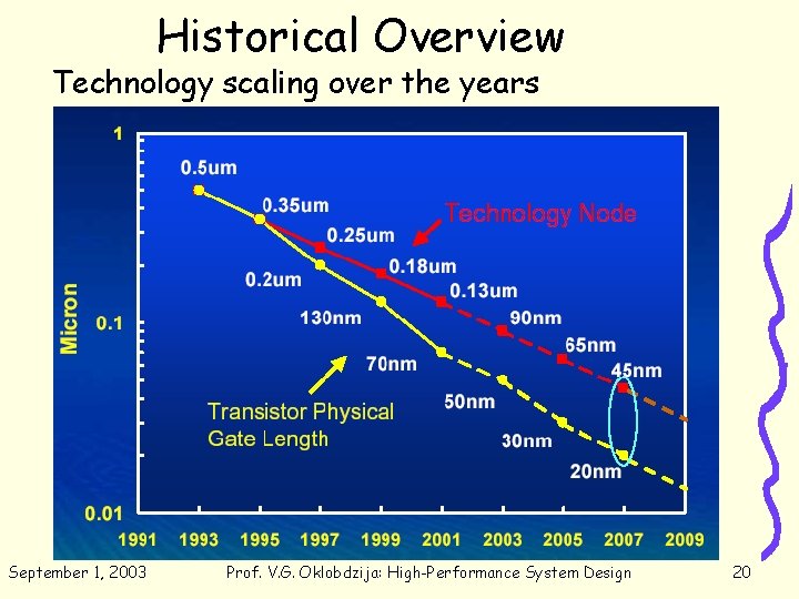
Historical Overview Technology scaling over the years September 1, 2003 Prof. V. G. Oklobdzija: High-Performance System Design 20
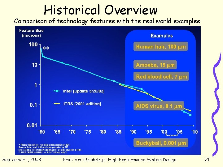
Historical Overview Comparison of technology features with the real world examples September 1, 2003 Prof. V. G. Oklobdzija: High-Performance System Design 21
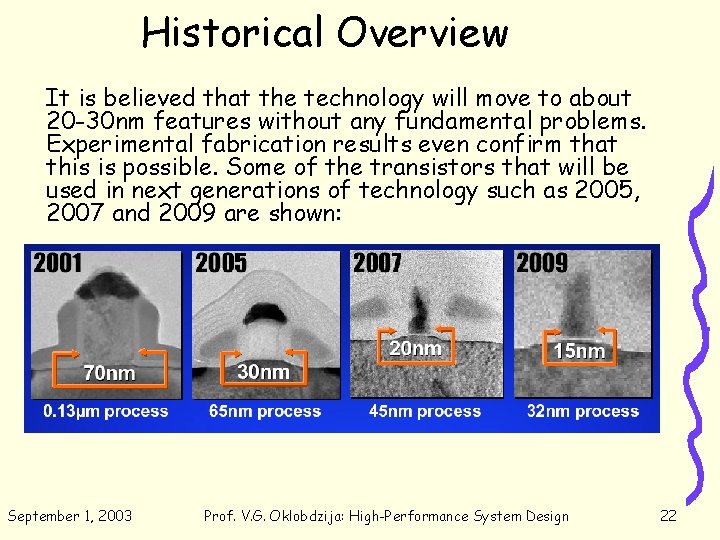
Historical Overview It is believed that the technology will move to about 20 -30 nm features without any fundamental problems. Experimental fabrication results even confirm that this is possible. Some of the transistors that will be used in next generations of technology such as 2005, 2007 and 2009 are shown: September 1, 2003 Prof. V. G. Oklobdzija: High-Performance System Design 22
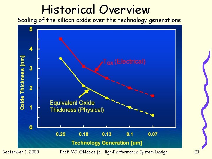
Historical Overview Scaling of the silicon oxide over the technology generations September 1, 2003 Prof. V. G. Oklobdzija: High-Performance System Design 23
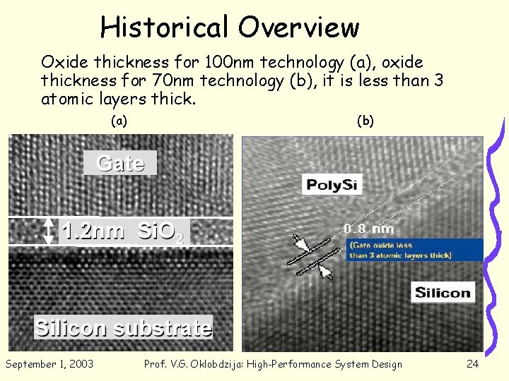
Historical Overview Oxide thickness for 100 nm technology (a), oxide thickness for 70 nm technology (b), it is less than 3 atomic layers thick. (a) September 1, 2003 (b) Prof. V. G. Oklobdzija: High-Performance System Design 24

Historical Overview: Future Experimental three-gate transistor structure (the channel is surrounded by the gate on all three sides) September 1, 2003 Prof. V. G. Oklobdzija: High-Performance System Design 25
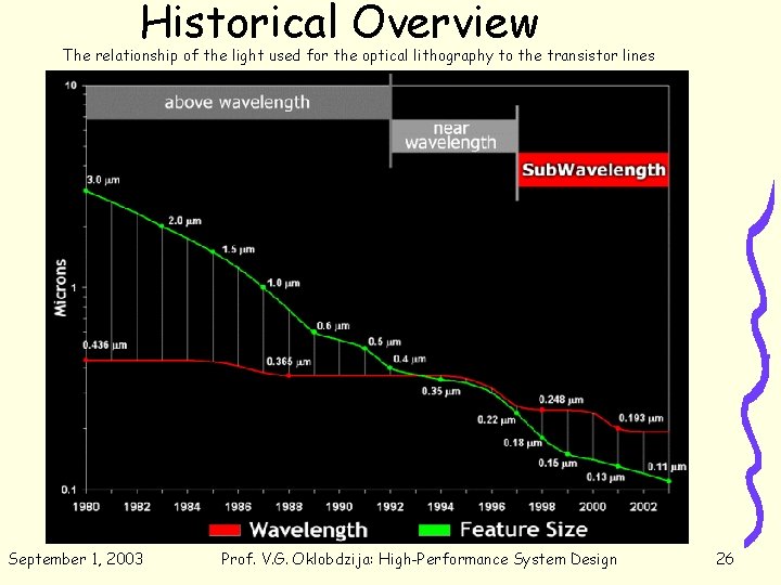
Historical Overview The relationship of the light used for the optical lithography to the transistor lines September 1, 2003 Prof. V. G. Oklobdzija: High-Performance System Design 26
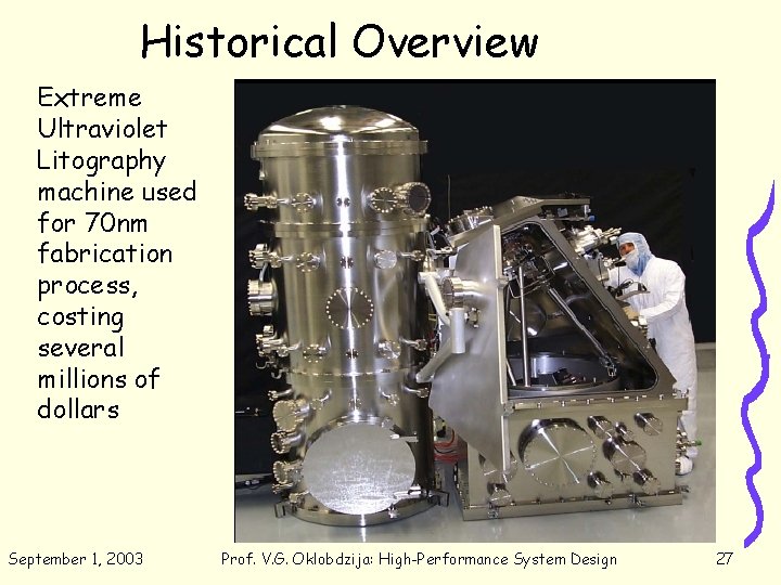
Historical Overview Extreme Ultraviolet Litography machine used for 70 nm fabrication process, costing several millions of dollars September 1, 2003 Prof. V. G. Oklobdzija: High-Performance System Design 27

Historical Overview Total power consumption increase in the world due to personal computer CPU chips only September 1, 2003 Prof. V. G. Oklobdzija: High-Performance System Design 28
- Slides: 28