Highlevel Power Reduction and Management Copyright Agarwal Srivaths

![Gated Clock Architecture : Redundant Clocking Detection q Idea [Ohnishi 97]: ■ Redundant clockings Gated Clock Architecture : Redundant Clocking Detection q Idea [Ohnishi 97]: ■ Redundant clockings](https://slidetodoc.com/presentation_image_h2/65979bd7d649971a044aaad450fd3d1d/image-6.jpg)
![Pre-computation q [Devadas 95] An Example ■ N-bit comparator ■ Pre-computation circuit based on Pre-computation q [Devadas 95] An Example ■ N-bit comparator ■ Pre-computation circuit based on](https://slidetodoc.com/presentation_image_h2/65979bd7d649971a044aaad450fd3d1d/image-16.jpg)
![Performance Optimization Transformations on an Example Behavior [Chandraskan 95] q Example Behavior of an Performance Optimization Transformations on an Example Behavior [Chandraskan 95] q Example Behavior of an](https://slidetodoc.com/presentation_image_h2/65979bd7d649971a044aaad450fd3d1d/image-27.jpg)
![Transformation (3): Pipelining Source: [Chandraskan 95] Copyright Agarwal & Srivaths, 2007 Low-Power Design and Transformation (3): Pipelining Source: [Chandraskan 95] Copyright Agarwal & Srivaths, 2007 Low-Power Design and](https://slidetodoc.com/presentation_image_h2/65979bd7d649971a044aaad450fd3d1d/image-32.jpg)
![Common Case Computation: A Power. Optimization Technique [Lakshminarayana 99] q Recall Amdahl’s law ! Common Case Computation: A Power. Optimization Technique [Lakshminarayana 99] q Recall Amdahl’s law !](https://slidetodoc.com/presentation_image_h2/65979bd7d649971a044aaad450fd3d1d/image-33.jpg)
![CCC: Example [Lakshminarayana 99] GCD Behavior STG annotated with state and state transition probabilities CCC: Example [Lakshminarayana 99] GCD Behavior STG annotated with state and state transition probabilities](https://slidetodoc.com/presentation_image_h2/65979bd7d649971a044aaad450fd3d1d/image-34.jpg)
![CCC: Example [Lakshminarayana 99] Identified common case behavior if (x != y) { if CCC: Example [Lakshminarayana 99] Identified common case behavior if (x != y) { if](https://slidetodoc.com/presentation_image_h2/65979bd7d649971a044aaad450fd3d1d/image-35.jpg)
![Operation Reduction: Distributivity [Chandrakasan 95] Reducing operations reduces the switched order polynomial example capacitance Operation Reduction: Distributivity [Chandrakasan 95] Reducing operations reduces the switched order polynomial example capacitance](https://slidetodoc.com/presentation_image_h2/65979bd7d649971a044aaad450fd3d1d/image-38.jpg)
![Operation Reduction: Distributivity [Chandrakasan 95] q 3 rd Reducing operations reduces the switched capacitance Operation Reduction: Distributivity [Chandrakasan 95] q 3 rd Reducing operations reduces the switched capacitance](https://slidetodoc.com/presentation_image_h2/65979bd7d649971a044aaad450fd3d1d/image-39.jpg)
![Power Supply Gating: An Example [OMAP-ISSCC 05] 90 nm OMAP 2420 So. C Power Power Supply Gating: An Example [OMAP-ISSCC 05] 90 nm OMAP 2420 So. C Power](https://slidetodoc.com/presentation_image_h2/65979bd7d649971a044aaad450fd3d1d/image-45.jpg)
![Power Supply Gating: An Example [OMAPISSCC 05] q Leakage currents compared between ■ All Power Supply Gating: An Example [OMAPISSCC 05] q Leakage currents compared between ■ All](https://slidetodoc.com/presentation_image_h2/65979bd7d649971a044aaad450fd3d1d/image-46.jpg)
![Data Retention Integrated Scan Retention Courtesy: [Zyuban-ISLPED 02] Save and Restore Operations Copyright Agarwal Data Retention Integrated Scan Retention Courtesy: [Zyuban-ISLPED 02] Save and Restore Operations Copyright Agarwal](https://slidetodoc.com/presentation_image_h2/65979bd7d649971a044aaad450fd3d1d/image-49.jpg)
![References q Survey Papers ■ [Devadas 95] S. Devadas, S. Malik: A Survey of References q Survey Papers ■ [Devadas 95] S. Devadas, S. Malik: A Survey of](https://slidetodoc.com/presentation_image_h2/65979bd7d649971a044aaad450fd3d1d/image-50.jpg)
- Slides: 50

High-level Power Reduction and Management Copyright Agarwal & Srivaths, 2007 Low-Power Design and Test, Lecture 7

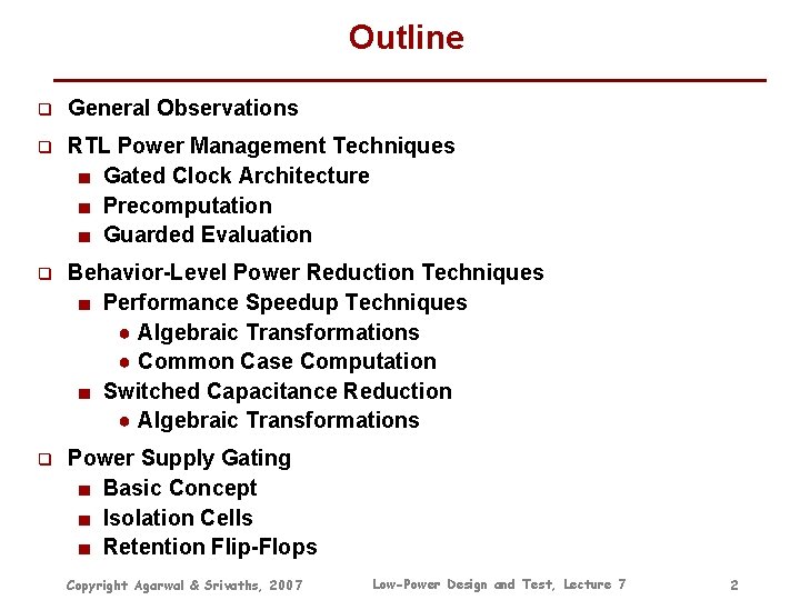
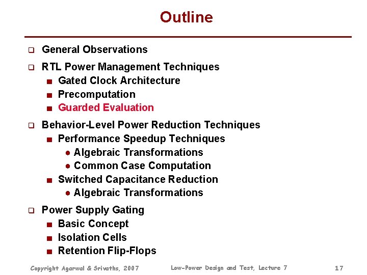
Outline q General Observations q RTL Power Management Techniques ■ Gated Clock Architecture ■ Precomputation ■ Guarded Evaluation q Behavior-Level Power Reduction Techniques ■ Performance Speedup Techniques ● Algebraic Transformations ● Common Case Computation ■ Switched Capacitance Reduction ● Algebraic Transformations q Power Supply Gating ■ Basic Concept ■ Isolation Cells ■ Retention Flip-Flops Copyright Agarwal & Srivaths, 2007 Low-Power Design and Test, Lecture 7 2

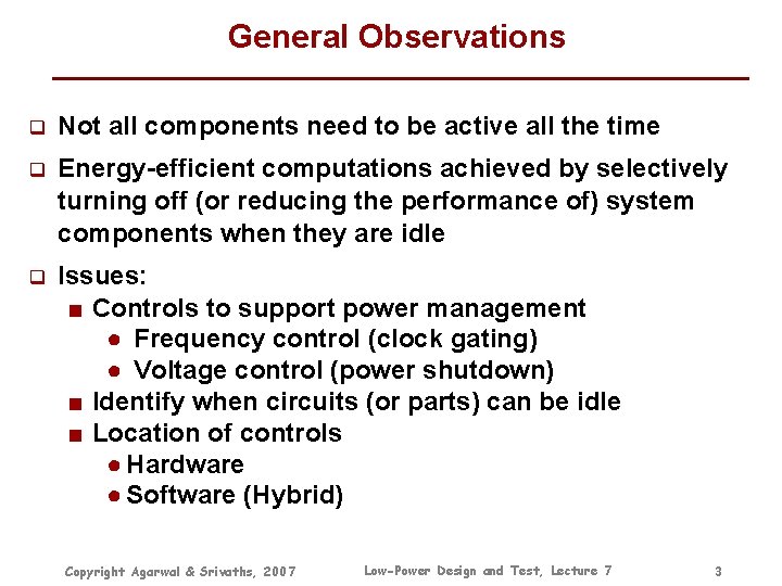
General Observations q Not all components need to be active all the time q Energy-efficient computations achieved by selectively turning off (or reducing the performance of) system components when they are idle q Issues: ■ Controls to support power management ● Frequency control (clock gating) ● Voltage control (power shutdown) ■ Identify when circuits (or parts) can be idle ■ Location of controls ● Hardware ● Software (Hybrid) Copyright Agarwal & Srivaths, 2007 Low-Power Design and Test, Lecture 7 3

Outline q General Observations q RTL Power Management Techniques ■ Gated Clock Architecture ■ Precomputation ■ Guarded Evaluation q Behavior-Level Power Reduction Techniques ■ Performance Speedup Techniques ● Algebraic Transformations ● Common Case Computation ■ Switched Capacitance Reduction ● Algebraic Transformations q Power Supply Gating ■ Basic Concept ■ Isolation Cells ■ Retention Flip-Flops Copyright Agarwal & Srivaths, 2007 Low-Power Design and Test, Lecture 7 4

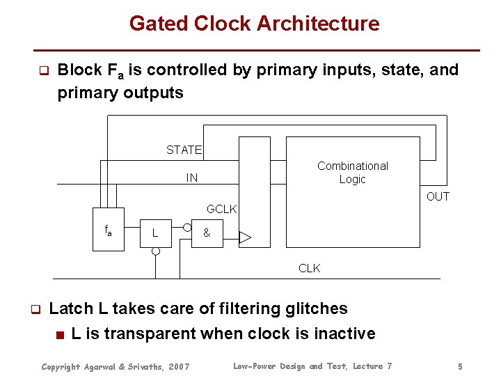
Gated Clock Architecture q Block Fa is controlled by primary inputs, state, and primary outputs STATE Combinational Logic IN OUT GCLK fa L & CLK q Latch L takes care of filtering glitches ■ L is transparent when clock is inactive Copyright Agarwal & Srivaths, 2007 Low-Power Design and Test, Lecture 7 5
![Gated Clock Architecture Redundant Clocking Detection q Idea Ohnishi 97 Redundant clockings Gated Clock Architecture : Redundant Clocking Detection q Idea [Ohnishi 97]: ■ Redundant clockings](https://slidetodoc.com/presentation_image_h2/65979bd7d649971a044aaad450fd3d1d/image-6.jpg)
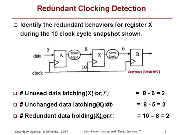
Gated Clock Architecture : Redundant Clocking Detection q Idea [Ohnishi 97]: ■ Redundant clockings activate registers unnecessarily ■ Use application profiles to detect redundant clockings ● Difference in the numbers of incoming and outgoing data of a register ■ Gated clock scheme designed using this information q Redundant behaviors of a register ■ Unused data latching: Data not transferred to a destination ■ Unchanged data latching: Register re-stores data already present from source ■ Redundant data holding: Register re-stores data Low-Power Design and Test, Lecture 7 Copyright Agarwal & Srivaths, 2007 6

Redundant Clocking Detection q Identify the redundant behaviors for register X during the 10 clock cycle snapshot shown. Courtesy: [Ohnishi 97] q # Unused data latching(X) or = 8 -6=2 q # Unchanged data latching(X) or = 8 -5=3 q # Redundant data holding(X) or = 10 – 8 = 2 Copyright Agarwal & Srivaths, 2007 Low-Power Design and Test, Lecture 7 7

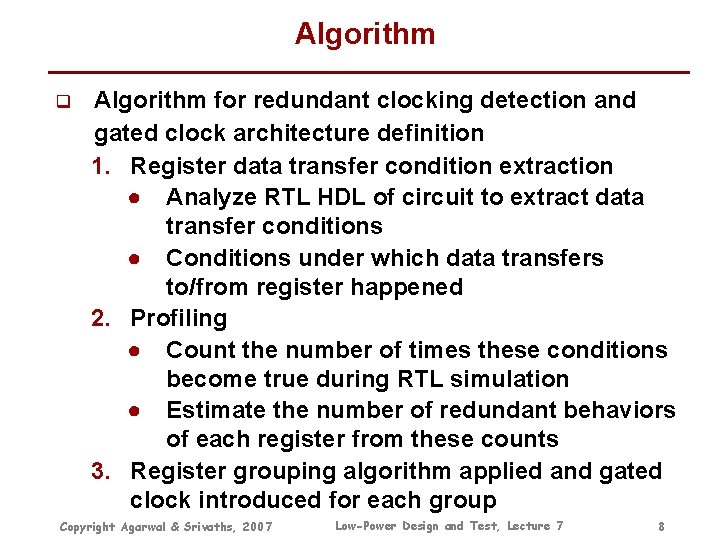
Algorithm q Algorithm for redundant clocking detection and gated clock architecture definition 1. Register data transfer condition extraction ● Analyze RTL HDL of circuit to extract data transfer conditions ● Conditions under which data transfers to/from register happened 2. Profiling ● Count the number of times these conditions become true during RTL simulation ● Estimate the number of redundant behaviors of each register from these counts 3. Register grouping algorithm applied and gated clock introduced for each group Copyright Agarwal & Srivaths, 2007 Low-Power Design and Test, Lecture 7 8

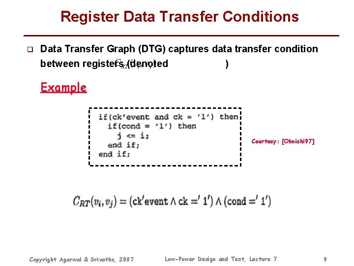
Register Data Transfer Conditions q Data Transfer Graph (DTG) captures data transfer condition between registers (denoted ) Example Courtesy: [Ohnishi 97] Copyright Agarwal & Srivaths, 2007 Low-Power Design and Test, Lecture 7 9

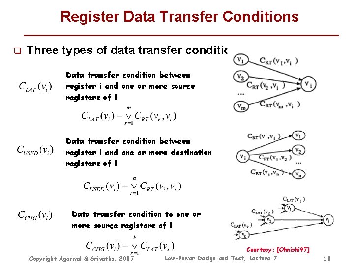
Register Data Transfer Conditions q Three types of data transfer conditions Data transfer condition between register i and one or more source registers of i Data transfer condition between register i and one or more destination registers of i Data transfer condition to one or more source registers of i Copyright Agarwal & Srivaths, 2007 Courtesy: [Ohnishi 97] Low-Power Design and Test, Lecture 7 10

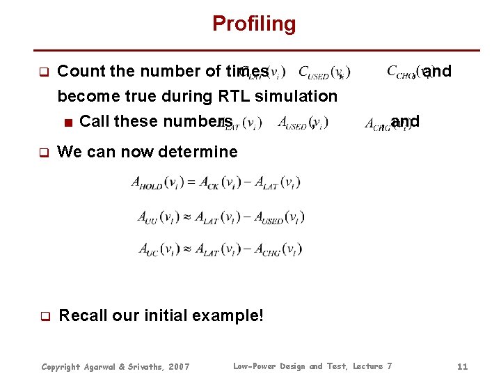
Profiling q Count the number of times , become true during RTL simulation ■ Call these numbers , q We can now determine q Recall our initial example! Copyright Agarwal & Srivaths, 2007 , and Low-Power Design and Test, Lecture 7 11

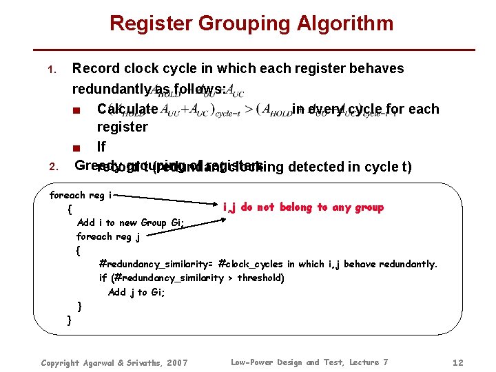
Register Grouping Algorithm 1. 2. Record clock cycle in which each register behaves redundantly as follows: ■ Calculate in every cycle for each register ■ If Greedy grouping of registers record t (redundant clocking detected in cycle t) foreach reg i i, j do not belong to any group { Add i to new Group Gi; foreach reg j { #redundancy_similarity= #clock_cycles in which i, j behave redundantly. if (#redundancy_similarity > threshold) Add j to Gi; } } Copyright Agarwal & Srivaths, 2007 Low-Power Design and Test, Lecture 7 12

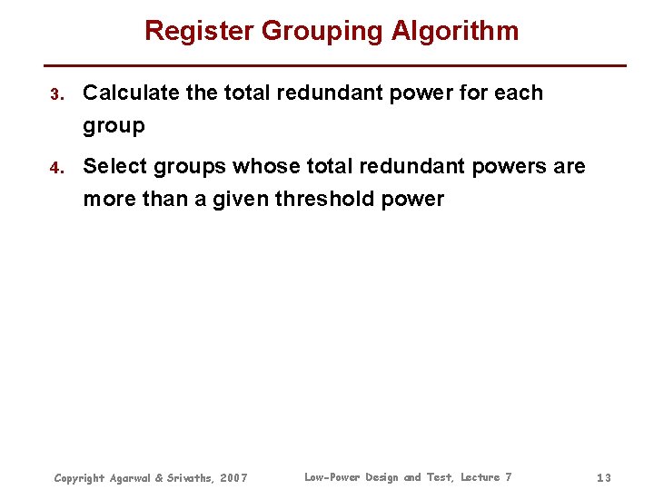
Register Grouping Algorithm 3. Calculate the total redundant power for each group 4. Select groups whose total redundant powers are more than a given threshold power Copyright Agarwal & Srivaths, 2007 Low-Power Design and Test, Lecture 7 13

Outline q General Observations q RTL Power Management Techniques ■ Gated Clock Architecture ■ Precomputation ■ Guarded Evaluation q Behavior-Level Power Reduction Techniques ■ Performance Speedup Techniques ● Algebraic Transformations ● Common Case Computation ■ Switched Capacitance Reduction ● Algebraic Transformations q Power Supply Gating ■ Basic Concept ■ Isolation Cells ■ Retention Flip-Flops Copyright Agarwal & Srivaths, 2007 Low-Power Design and Test, Lecture 7 14

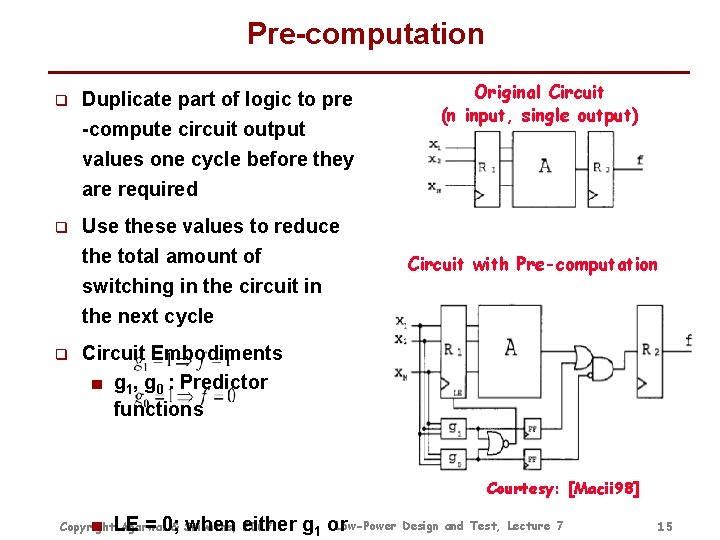
Pre-computation q Duplicate part of logic to pre -compute circuit output values one cycle before they are required q Use these values to reduce the total amount of switching in the circuit in the next cycle q Original Circuit (n input, single output) Circuit with Pre-computation Circuit Embodiments ■ g 1, g 0 : Predictor functions Courtesy: [Macii 98] Low-Power Design and Test, Lecture 7 ■ LE = 0; when either g 1 or Copyright Agarwal & Srivaths, 2007 15
![Precomputation q Devadas 95 An Example Nbit comparator Precomputation circuit based on Pre-computation q [Devadas 95] An Example ■ N-bit comparator ■ Pre-computation circuit based on](https://slidetodoc.com/presentation_image_h2/65979bd7d649971a044aaad450fd3d1d/image-16.jpg)
Pre-computation q [Devadas 95] An Example ■ N-bit comparator ■ Pre-computation circuit based on the behavior of the comparison operation ● If the MSBs of C and D are not equal, C>D can be evaluated just using the MSBs ● Otherwise, the rest of the bits (of C and D) are also needed. ■ Therefore, LE is given by Copyright Agarwal & Srivaths, 2007 Comparator Circuit XNOR Comparator Circuit with pre-computation Low-Power Design and Test, Lecture 7 16

Outline q General Observations q RTL Power Management Techniques ■ Gated Clock Architecture ■ Precomputation ■ Guarded Evaluation q Behavior-Level Power Reduction Techniques ■ Performance Speedup Techniques ● Algebraic Transformations ● Common Case Computation ■ Switched Capacitance Reduction ● Algebraic Transformations q Power Supply Gating ■ Basic Concept ■ Isolation Cells ■ Retention Flip-Flops Copyright Agarwal & Srivaths, 2007 Low-Power Design and Test, Lecture 7 17

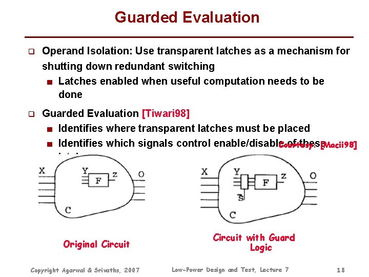
Guarded Evaluation q Operand Isolation: Use transparent latches as a mechanism for shutting down redundant switching ■ Latches enabled when useful computation needs to be done q Guarded Evaluation [Tiwari 98] ■ Identifies where transparent latches must be placed ■ Identifies which signals control enable/disable of these Courtesy: [Macii 98] latches Original Circuit Copyright Agarwal & Srivaths, 2007 Circuit with Guard Logic Low-Power Design and Test, Lecture 7 18

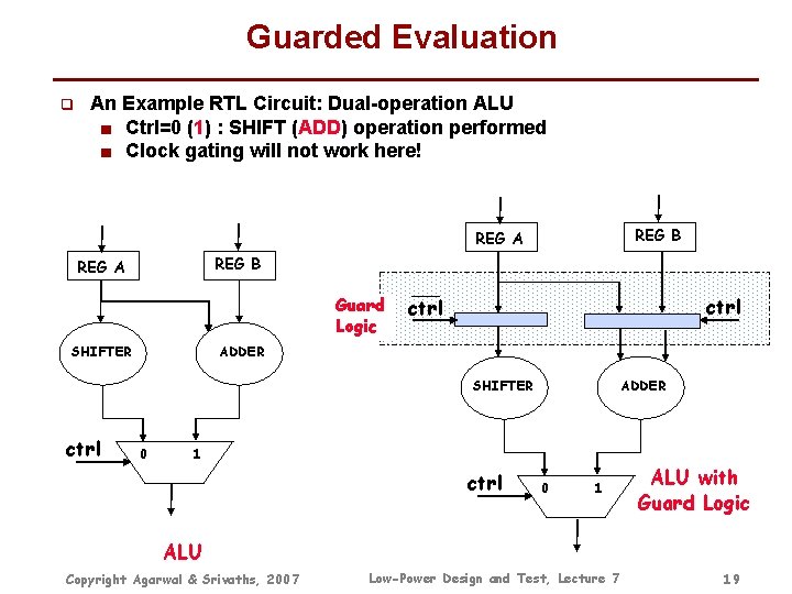
Guarded Evaluation q An Example RTL Circuit: Dual-operation ALU ■ Ctrl=0 (1) : SHIFT (ADD) operation performed ■ Clock gating will not work here! REG B REG A Guard Logic SHIFTER ctrl ADDER SHIFTER ctrl 0 ADDER 1 ctrl 0 1 ALU with Guard Logic ALU Copyright Agarwal & Srivaths, 2007 Low-Power Design and Test, Lecture 7 19

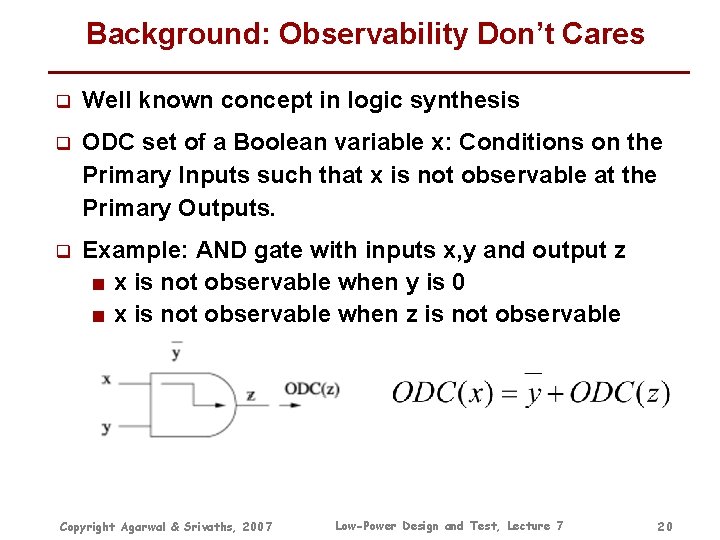
Background: Observability Don’t Cares q Well known concept in logic synthesis q ODC set of a Boolean variable x: Conditions on the Primary Inputs such that x is not observable at the Primary Outputs. q Example: AND gate with inputs x, y and output z ■ x is not observable when y is 0 ■ x is not observable when z is not observable Copyright Agarwal & Srivaths, 2007 Low-Power Design and Test, Lecture 7 20

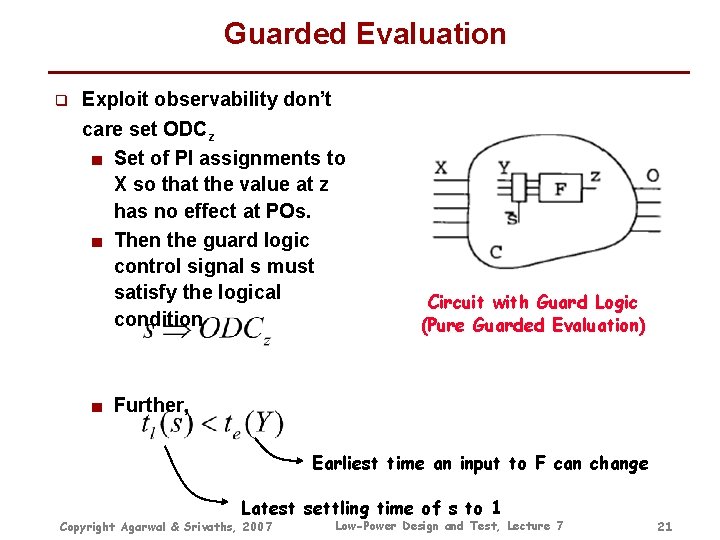
Guarded Evaluation q Exploit observability don’t care set ODCz ■ Set of PI assignments to X so that the value at z has no effect at POs. ■ Then the guard logic control signal s must satisfy the logical condition Circuit with Guard Logic (Pure Guarded Evaluation) ■ Further, Earliest time an input to F can change Latest settling time of s to 1 Copyright Agarwal & Srivaths, 2007 Low-Power Design and Test, Lecture 7 21

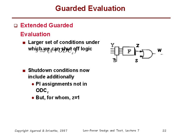
Guarded Evaluation q Extended Guarded Evaluation ■ Larger set of conditions under which we can shut off logic z w s ■ Shutdown conditions now include additionally ● PI assignments not in ODCz ● But, for whom, z=1 Copyright Agarwal & Srivaths, 2007 Low-Power Design and Test, Lecture 7 22

Outline q General Observations q RTL Power Management Techniques ■ Gated Clock Architecture ■ Precomputation ■ Guarded Evaluation q Behavior-Level Power Reduction Techniques ■ Performance Speedup Techniques ● Algebraic Transformations ● Common Case Computation ■ Switched Capacitance Reduction ● Algebraic Transformations q Power Supply Gating ■ Basic Concept ■ Isolation Cells ■ Retention Flip-Flops Copyright Agarwal & Srivaths, 2007 Low-Power Design and Test, Lecture 7 23

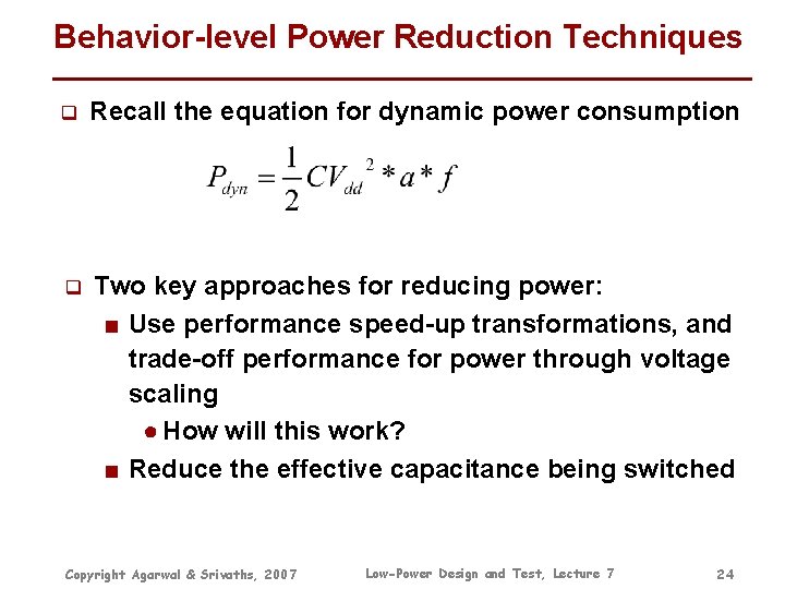
Behavior-level Power Reduction Techniques q Recall the equation for dynamic power consumption q Two key approaches for reducing power: ■ Use performance speed-up transformations, and trade-off performance for power through voltage scaling ● How will this work? ■ Reduce the effective capacitance being switched Copyright Agarwal & Srivaths, 2007 Low-Power Design and Test, Lecture 7 24

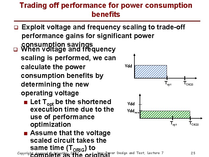
Trading off performance for power consumption benefits q q Exploit voltage and frequency scaling to trade-off performance gains for significant power consumption savings When voltage and frequency scaling is performed, we can Vdd calculate the power consumption benefits by T T determining the new operating voltage ■ Let Topt be the shortened Vdd execution time due to the Vdd use of performance T optimization ■ Assume that the voltage scaled circuit takes the same time (TORIG) to opt ORIG new opt Copyright Agarwal & Srivaths, 2007 Low-Power Design and Test, Lecture 7 TORIG 25

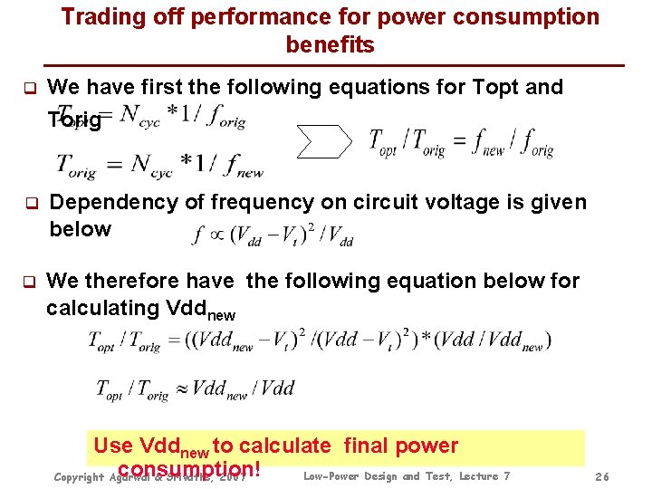
Trading off performance for power consumption benefits q We have first the following equations for Topt and Torig q Dependency of frequency on circuit voltage is given below q We therefore have the following equation below for calculating Vddnew Use Vddnew to calculate final power consumption! Low-Power Design and Test, Lecture 7 Copyright Agarwal & Srivaths, 2007 26
![Performance Optimization Transformations on an Example Behavior Chandraskan 95 q Example Behavior of an Performance Optimization Transformations on an Example Behavior [Chandraskan 95] q Example Behavior of an](https://slidetodoc.com/presentation_image_h2/65979bd7d649971a044aaad450fd3d1d/image-27.jpg)
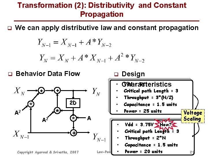
Performance Optimization Transformations on an Example Behavior [Chandraskan 95] q Example Behavior of an IIR Filter q Behavior Data Flow + * D A Copyright Agarwal & Srivaths, 2007 q • • • Design Characteristics Vdd = 5 V Critical path Length = 2 Throughput = 2*N Capacitance = 1 unit Power = 25 units Low-Power Design and Test, Lecture 7 27

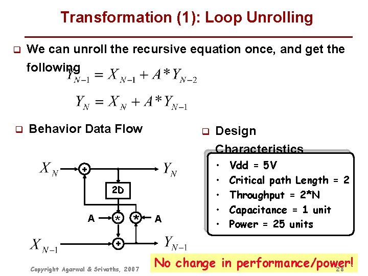
Transformation (1): Loop Unrolling q We can unroll the recursive equation once, and get the following q Behavior Data Flow q + 2 D A * * A Design Characteristics • • • Vdd = 5 V Critical path Length = 2 Throughput = 2*N Capacitance = 1 unit Power = 25 units + Copyright Agarwal & Srivaths, 2007 No Low-Power change in performance/power! Design and Test, Lecture 7 28

Transformation (2): Distributivity and Constant Propagation q We can apply distributive law and constant propagation q Behavior Data Flow + A 2 q • • • + 2 D * A 2 * * A + Copyright Agarwal & Srivaths, 2007 Low-Power Design Vdd = 5 V Characteristics Critical path Length = 3 Throughput = 3*(N/2) Capacitance = 1. 5 units Power = 25 units • Vdd = 3. 75 V How? • Critical path Length = 3 • Throughput = 2*N • Capacitance = 1. 5 units • Power = 20 units 7 Design and Test, Lecture Voltage Scaling 29

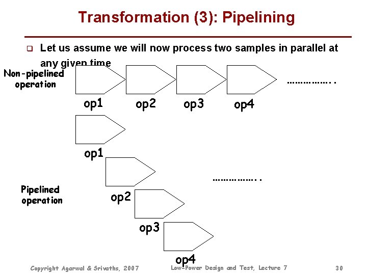
Transformation (3): Pipelining q Let us assume we will now process two samples in parallel at any given time Non-pipelined operation ……………. . op 1 op 2 op 3 op 4 op 1 Pipelined operation ……………. . op 2 op 3 Copyright Agarwal & Srivaths, 2007 op 4 Low-Power Design and Test, Lecture 7 30

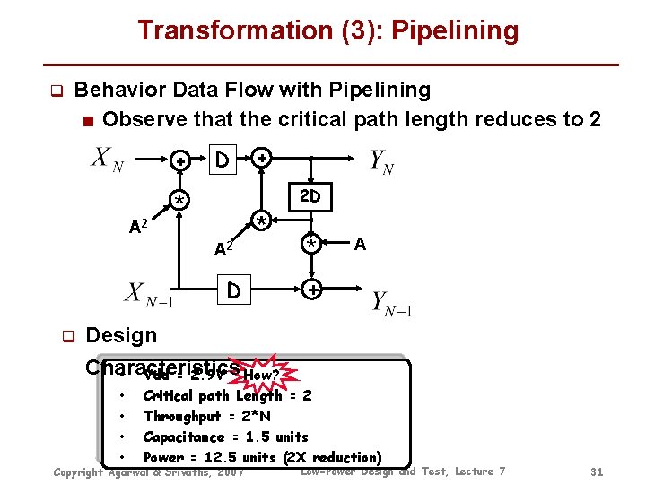
Transformation (3): Pipelining q Behavior Data Flow with Pipelining ■ Observe that the critical path length reduces to 2 + A 2 D + 2 D * A 2 * D q * A + Design Characteristics • Vdd = 2. 9 V How? • • Critical path Length = 2 Throughput = 2*N Capacitance = 1. 5 units Power = 12. 5 units (2 X reduction) Copyright Agarwal & Srivaths, 2007 Low-Power Design and Test, Lecture 7 31
![Transformation 3 Pipelining Source Chandraskan 95 Copyright Agarwal Srivaths 2007 LowPower Design and Transformation (3): Pipelining Source: [Chandraskan 95] Copyright Agarwal & Srivaths, 2007 Low-Power Design and](https://slidetodoc.com/presentation_image_h2/65979bd7d649971a044aaad450fd3d1d/image-32.jpg)
Transformation (3): Pipelining Source: [Chandraskan 95] Copyright Agarwal & Srivaths, 2007 Low-Power Design and Test, Lecture 7 32
![Common Case Computation A Power Optimization Technique Lakshminarayana 99 q Recall Amdahls law Common Case Computation: A Power. Optimization Technique [Lakshminarayana 99] q Recall Amdahl’s law !](https://slidetodoc.com/presentation_image_h2/65979bd7d649971a044aaad450fd3d1d/image-33.jpg)
Common Case Computation: A Power. Optimization Technique [Lakshminarayana 99] q Recall Amdahl’s law ! q Idea ■ Identify computations or sequence of computations in behavior that occur most frequently ■ Design separate circuit that implements common-case behavior Copyright Agarwal & Srivaths, 2007 Generic Architecture ORIGINAL CIRCUIT Common-case Detection & execution circuit Activity of energy optimized circuit Low-Power Design and Test, Lecture 7 33
![CCC Example Lakshminarayana 99 GCD Behavior STG annotated with state and state transition probabilities CCC: Example [Lakshminarayana 99] GCD Behavior STG annotated with state and state transition probabilities](https://slidetodoc.com/presentation_image_h2/65979bd7d649971a044aaad450fd3d1d/image-34.jpg)
CCC: Example [Lakshminarayana 99] GCD Behavior STG annotated with state and state transition probabilities from simulation profiles while (x != y) { if (x > y) { x : = x - y; } else { y : = y - x; } } Copyright Agarwal & Srivaths, 2007 Low-Power Design and Test, Lecture 7 34
![CCC Example Lakshminarayana 99 Identified common case behavior if x y if CCC: Example [Lakshminarayana 99] Identified common case behavior if (x != y) { if](https://slidetodoc.com/presentation_image_h2/65979bd7d649971a044aaad450fd3d1d/image-35.jpg)
CCC: Example [Lakshminarayana 99] Identified common case behavior if (x != y) { if (x > y) { x : = x -y; }} Tempx : = x - 4 y; if (Tempx > 0) { x : = Tempx; } y x Common Case Execution Copyright Agarwal & Srivaths, 2007 Simplified common case behavior 2 Common Case Detection 0 Low-Power Design and Test, Lecture 7 35

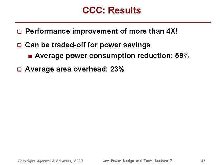
CCC: Results q Performance improvement of more than 4 X! q Can be traded-off for power savings ■ Average power consumption reduction: 59% q Average area overhead: 23% Copyright Agarwal & Srivaths, 2007 Low-Power Design and Test, Lecture 7 36

Outline q General Observations q RTL Power Management Techniques ■ Gated Clock Architecture ■ Precomputation ■ Guarded Evaluation q Behavior-Level Power Reduction Techniques ■ Performance Speedup Techniques ● Algebraic Transformations ● Common Case Computation ■ Switched Capacitance Reduction ● Algebraic Transformations q Power Supply Gating ■ Basic Concept ■ Isolation Cells ■ Retention Flip-Flops Copyright Agarwal & Srivaths, 2007 Low-Power Design and Test, Lecture 7 37
![Operation Reduction Distributivity Chandrakasan 95 Reducing operations reduces the switched order polynomial example capacitance Operation Reduction: Distributivity [Chandrakasan 95] Reducing operations reduces the switched order polynomial example capacitance](https://slidetodoc.com/presentation_image_h2/65979bd7d649971a044aaad450fd3d1d/image-38.jpg)
Operation Reduction: Distributivity [Chandrakasan 95] Reducing operations reduces the switched order polynomial example capacitance q 2 nd can be rewritten as X X A * + X + A * * + X B B X q One lesser multiplication! q Same throughput q No change to the critical path Copyright Agarwal & Srivaths, 2007 + Low-Power Design and Test, Lecture 7 38
![Operation Reduction Distributivity Chandrakasan 95 q 3 rd Reducing operations reduces the switched capacitance Operation Reduction: Distributivity [Chandrakasan 95] q 3 rd Reducing operations reduces the switched capacitance](https://slidetodoc.com/presentation_image_h2/65979bd7d649971a044aaad450fd3d1d/image-39.jpg)
Operation Reduction: Distributivity [Chandrakasan 95] q 3 rd Reducing operations reduces the switched capacitance ■ Can also increase the critical path (can mean higher voltage to realize the same throughput) order polynomial example can be rewritten as A X * + + * X A + X B X + B + * * C #Operations=7 Critical path=4 Copyright Agarwal & Srivaths, 2007 #Operations=5 Critical path=5 Low-Power Design and Test, Lecture 7 * X + C 39

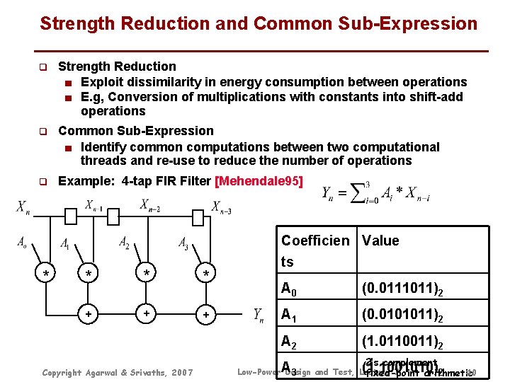
Strength Reduction and Common Sub-Expression q Strength Reduction ■ Exploit dissimilarity in energy consumption between operations ■ E. g, Conversion of multiplications with constants into shift-add operations q Common Sub-Expression ■ Identify common computations between two computational threads and re-use to reduce the number of operations q Example: 4 -tap FIR Filter [Mehendale 95] * * + + + Copyright Agarwal & Srivaths, 2007 Coefficien Value ts A 0 (0. 0111011)2 A 1 (0. 0101011)2 A 2 (1. 0110011)2 A 2’s complement (1. 1001010) Low-Power Design and Test, Lecture 7 3 2 40 fixed-point arithmetic

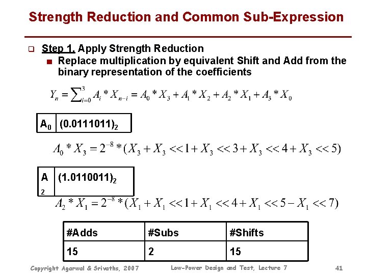
Strength Reduction and Common Sub-Expression q Step 1. Apply Strength Reduction ■ Replace multiplication by equivalent Shift and Add from the binary representation of the coefficients A 0 (0. 0111011)2 A (1. 0110011)2 2 #Adds #Subs #Shifts 15 2 15 Copyright Agarwal & Srivaths, 2007 Low-Power Design and Test, Lecture 7 41

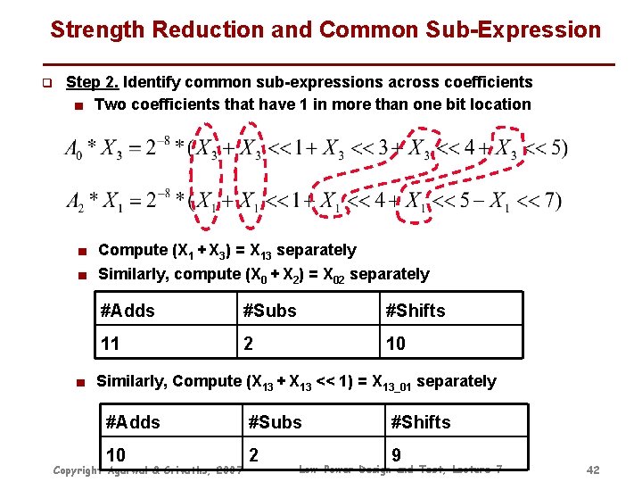
Strength Reduction and Common Sub-Expression q Step 2. Identify common sub-expressions across coefficients ■ Two coefficients that have 1 in more than one bit location ■ Compute (X 1 + X 3) = X 13 separately ■ Similarly, compute (X 0 + X 2) = X 02 separately #Adds #Subs #Shifts 11 2 10 ■ Similarly, Compute (X 13 + X 13 << 1) = X 13_01 separately #Adds #Subs #Shifts 10 2 9 Copyright Agarwal & Srivaths, 2007 Low-Power Design and Test, Lecture 7 42

Outline q General Observations q RTL Power Management Techniques ■ Gated Clock Architecture ■ Precomputation ■ Guarded Evaluation q Behavior-Level Power Reduction Techniques ■ Performance Speedup Techniques ● Algebraic Transformations ● Common Case Computation ■ Switched Capacitance Reduction ● Algebraic Transformations q Power Supply Gating ■ Power Switches ■ Isolation Cells ■ Retention Flip-Flops Copyright Agarwal & Srivaths, 2007 Low-Power Design and Test, Lecture 7 43

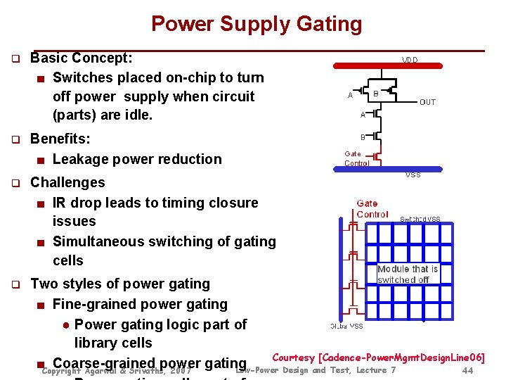
Power Supply Gating q Basic Concept: ■ Switches placed on-chip to turn off power supply when circuit (parts) are idle. q Benefits: ■ Leakage power reduction q Challenges ■ IR drop leads to timing closure issues ■ Simultaneous switching of gating cells q Two styles of power gating ■ Fine-grained power gating ● Power gating logic part of library cells Courtesy [Cadence-Power. Mgmt. Design. Line 06] ■Copyright Coarse-grained power gating Low-Power Design and Test, Lecture 7 Agarwal & Srivaths, 2007 44
![Power Supply Gating An Example OMAPISSCC 05 90 nm OMAP 2420 So C Power Power Supply Gating: An Example [OMAP-ISSCC 05] 90 nm OMAP 2420 So. C Power](https://slidetodoc.com/presentation_image_h2/65979bd7d649971a044aaad450fd3d1d/image-45.jpg)
Power Supply Gating: An Example [OMAP-ISSCC 05] 90 nm OMAP 2420 So. C Power Switch used in OMAP q 5 power domains in OMAP So. C enabled by power gating q Power switches gate VDD, consists of ■ Weak PMOS: Sinks low current for power restore ■ Strong PMOS: Deliver current for normal operation q 2 -pass power turn-on mechanism to prevent current surges ■ Weak switches turned on first to almost fully restore VDD(local), and then the strong switches are turned on to support normal operation Copyright Agarwal & Srivaths, 2007 Low-Power Design and Test, Lecture 7 45
![Power Supply Gating An Example OMAPISSCC 05 q Leakage currents compared between All Power Supply Gating: An Example [OMAPISSCC 05] q Leakage currents compared between ■ All](https://slidetodoc.com/presentation_image_h2/65979bd7d649971a044aaad450fd3d1d/image-46.jpg)
Power Supply Gating: An Example [OMAPISSCC 05] q Leakage currents compared between ■ All power domains ON ■ Wk. Up domain only ON q Nearly 40 X reduction seen at room temperature Copyright Agarwal & Srivaths, 2007 Low-Power Design and Test, Lecture 7 46

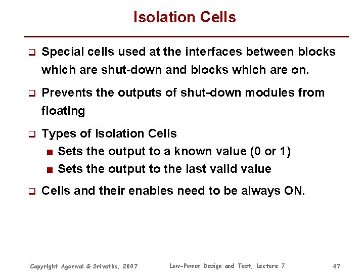
Isolation Cells q Special cells used at the interfaces between blocks which are shut-down and blocks which are on. q Prevents the outputs of shut-down modules from floating q Types of Isolation Cells ■ Sets the output to a known value (0 or 1) ■ Sets the output to the last valid value q Cells and their enables need to be always ON. Copyright Agarwal & Srivaths, 2007 Low-Power Design and Test, Lecture 7 47

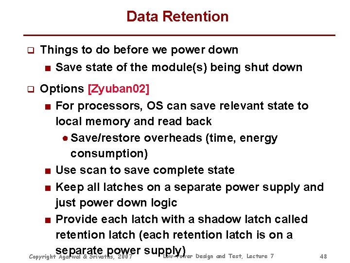
Data Retention q Things to do before we power down ■ Save state of the module(s) being shut down Options [Zyuban 02] ■ For processors, OS can save relevant state to local memory and read back ● Save/restore overheads (time, energy consumption) ■ Use scan to save complete state ■ Keep all latches on a separate power supply and just power down logic ■ Provide each latch with a shadow latch called retention latch (each retention latch is on a separate power supply) Low-Power Design and Test, Lecture 7 Copyright Agarwal & Srivaths, 2007 48 q
![Data Retention Integrated Scan Retention Courtesy ZyubanISLPED 02 Save and Restore Operations Copyright Agarwal Data Retention Integrated Scan Retention Courtesy: [Zyuban-ISLPED 02] Save and Restore Operations Copyright Agarwal](https://slidetodoc.com/presentation_image_h2/65979bd7d649971a044aaad450fd3d1d/image-49.jpg)
Data Retention Integrated Scan Retention Courtesy: [Zyuban-ISLPED 02] Save and Restore Operations Copyright Agarwal & Srivaths, 2007 Low-Power Design and Test, Lecture 7 49
![References q Survey Papers Devadas 95 S Devadas S Malik A Survey of References q Survey Papers ■ [Devadas 95] S. Devadas, S. Malik: A Survey of](https://slidetodoc.com/presentation_image_h2/65979bd7d649971a044aaad450fd3d1d/image-50.jpg)
References q Survey Papers ■ [Devadas 95] S. Devadas, S. Malik: A Survey of Optimization Techniques Targeting Low Power VLSI Circuits. DAC 1995: 242 -247 ■ [Macii 98] E. Macii, M. Pedram, F. Somenzi: High-level power modeling, estimation, and optimization. IEEE Trans. on CAD of Integrated Circuits and Systems 17(11): 1061 -1079 (1998) ■ [Chandrakasan 95 a] A. P. Chandrakasan, M. Potkonjak, R. Mehra, J. Rabaey, and R. Brodersen, ``Optimizing power using transformations, '' IEEE Trans. Computer-Aided Design, vol. 14, pp. 12 --31, Jan. 1995. q RTL Power Management ■ [Ohnishi 97] M. Ohnishi, A. Yamada, H. Noda, and T. Kambe, ``A Method of Redundant Clocking Detection and Power Reduction at the RTL level, '' in Proc. Int. Symp. Low Power Electronics & Design (ISLPED), pp. 131 -136, Aug. 1997. ■ [Tiwari 98] V. Tiwari, S. Malik, P. Ashar: Guarded evaluation: pushing power management to logic synthesis/design. IEEE Trans. on CAD of Integrated Circuits and Systems (TCAD) 17(10): 1051 -1060 (1998) q Behavioral Power Optimization ■ [Mehendale 95] M. Mehendale, S. D. Sherlekar, G. Venkatesh, “Synthesis of multiplier-less FIR filters with minimum number of additions”. ICCAD 1995: 668 -671 ■ [Lakshminarayana 99] G. Lakshminarayana, A. Raghunathan, K. S. Khouri, N. K. Jha, S. Dey: Common-Case Computation: A High-Level Technique for Power and Performance Optimization. DAC 1999: 56 -61 Power Supply Gating ■ [Cadence-Power. Mgmt. Design. Line 06] Anand Iyer, “Demystify power gating and stop leakage cold”, Power Management Design. Line, 03/03/06 ■ [Zyuban 02] V. Zyuban, S. V. Kosonocky: Low power integrated scan-retention mechanism. ISLPED 2002: 98 -102 ■ [OMAP-ISSCC 05] P. Royannez, H. Mair, F. Dahan, M. Wagner et. al. ; "90 nm Low Leakage So. C Design Techniques for Wireless Applications"; Low-Power ISSCC'05, Feb 2005 Design and Test, Lecture 7 Copyright Agarwal & Srivaths, 2007 50 q