HighDensity AcDc Power Supplies using ActiveClamp Flyback Topology

High-Density Ac-Dc Power Supplies using Active-Clamp Flyback Topology Ajay Hari, Bryan Mc. Coy
Agenda • Introduction to active-clamp flyback operation (ACF) • ACF light-load efficiency challenge • Introduction to the NCP 1568 – Ac-Dc ACF PWM IC. • Light load and standby solution • Design equations for transformer selection of the ACF • Primary and secondary component selection considerations • Performance data of ultra-high density active-clamp flyback board. 2
Introduction to Active-Clamp Flyback Operation (ACF) 3
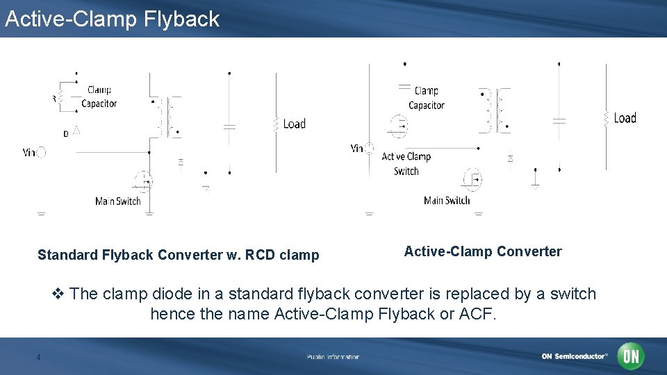
Active-Clamp Flyback Standard Flyback Converter w. RCD clamp Active-Clamp Converter v The clamp diode in a standard flyback converter is replaced by a switch hence the name Active-Clamp Flyback or ACF. 4
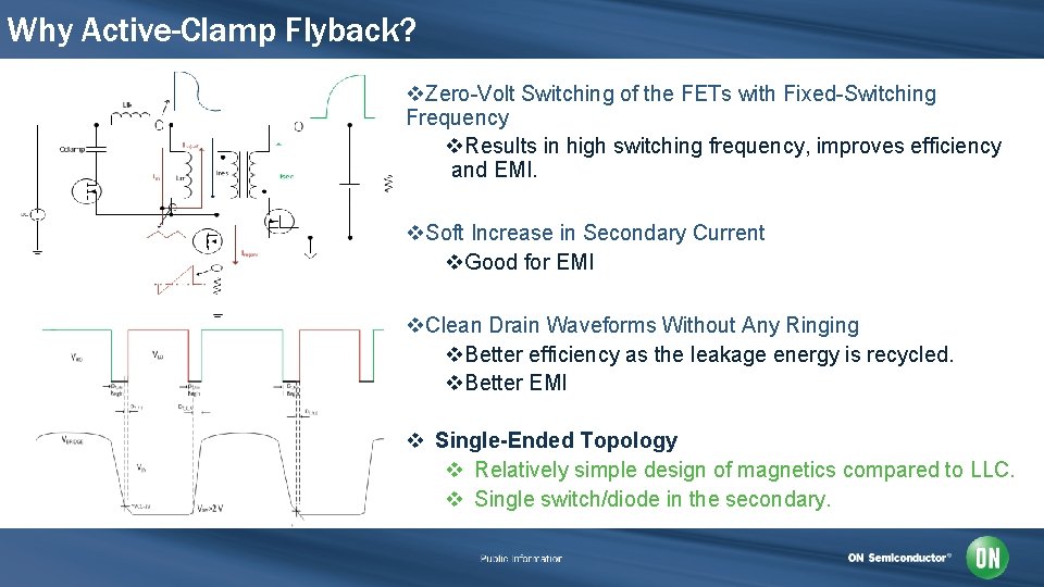
Why Active-Clamp Flyback? v. Zero-Volt Switching of the FETs with Fixed-Switching Frequency v. Results in high switching frequency, improves efficiency and EMI. v. Soft Increase in Secondary Current v. Good for EMI v. Clean Drain Waveforms Without Any Ringing v. Better efficiency as the leakage energy is recycled. v. Better EMI v Single-Ended Topology v Relatively simple design of magnetics compared to LLC. v Single switch/diode in the secondary.
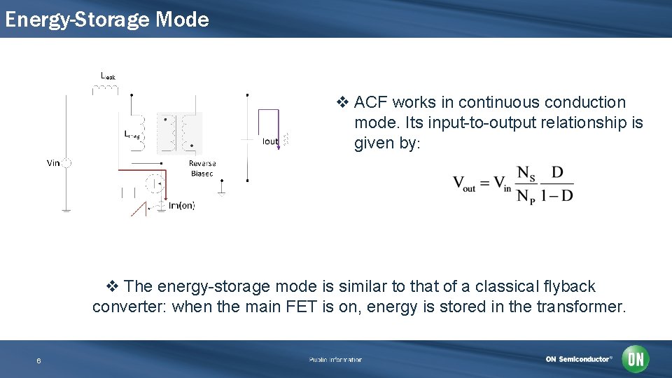
Energy-Storage Mode v ACF works in continuous conduction mode. Its input-to-output relationship is given by: v The energy-storage mode is similar to that of a classical flyback converter: when the main FET is on, energy is stored in the transformer. 6
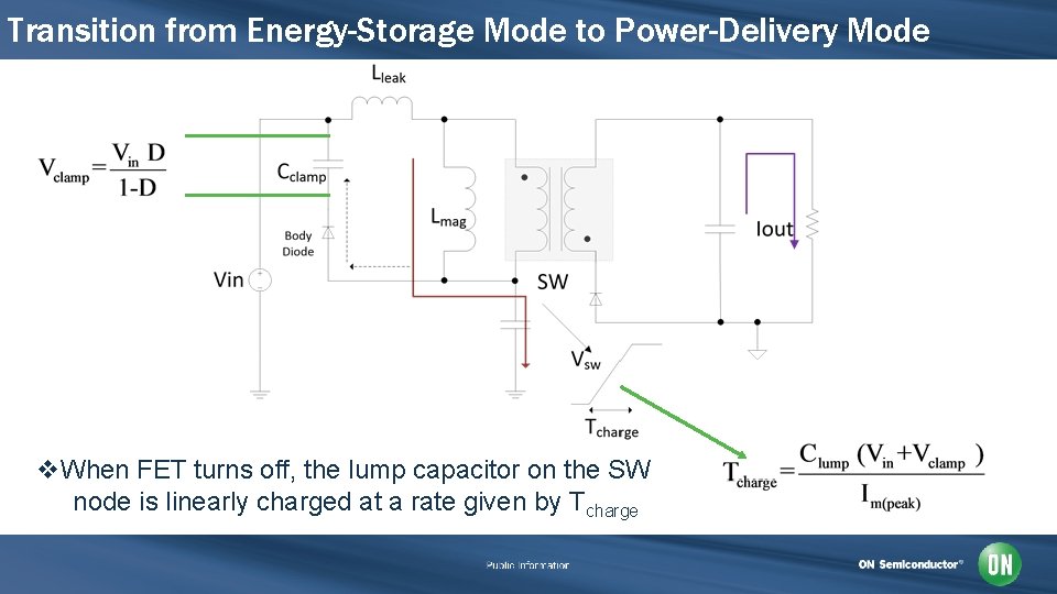
Transition from Energy-Storage Mode to Power-Delivery Mode v. When FET turns off, the lump capacitor on the SW node is linearly charged at a rate given by Tcharge
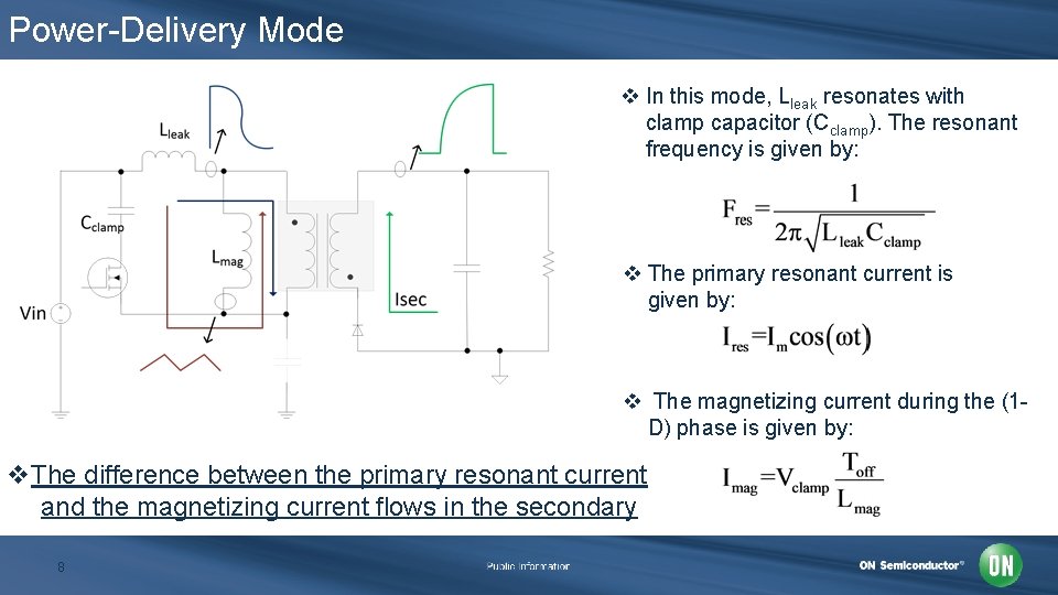
Power-Delivery Mode v In this mode, Lleak resonates with clamp capacitor (Cclamp). The resonant frequency is given by: v The primary resonant current is given by: v The magnetizing current during the (1 D) phase is given by: v. The difference between the primary resonant current and the magnetizing current flows in the secondary 8
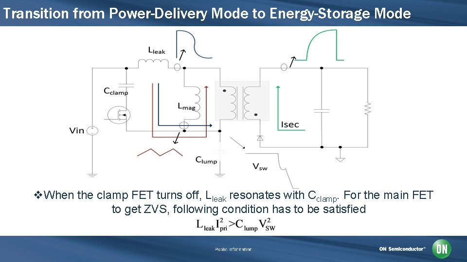
Transition from Power-Delivery Mode to Energy-Storage Mode v. When the clamp FET turns off, Lleak resonates with Cclamp. For the main FET to get ZVS, following condition has to be satisfied
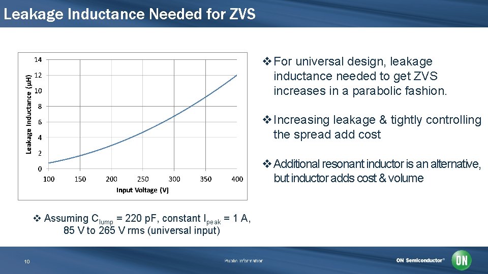
Leakage Inductance Needed for ZVS v. For universal design, leakage inductance needed to get ZVS increases in a parabolic fashion. v. Increasing leakage & tightly controlling the spread add cost v. Additional resonant inductor is an alternative, but inductor adds cost & volume v Assuming Clump = 220 p. F, constant Ipeak = 1 A, 85 V to 265 V rms (universal input) 10
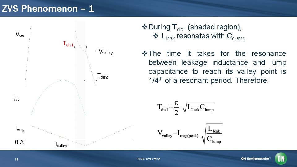
ZVS Phenomenon – 1 v. During Tdis 1 (shaded region), v Lleak resonates with Cclamp. v. The time it takes for the resonance between leakage inductance and lump capacitance to reach its valley point is 1/4 th of a resonant period. Therefore: 11
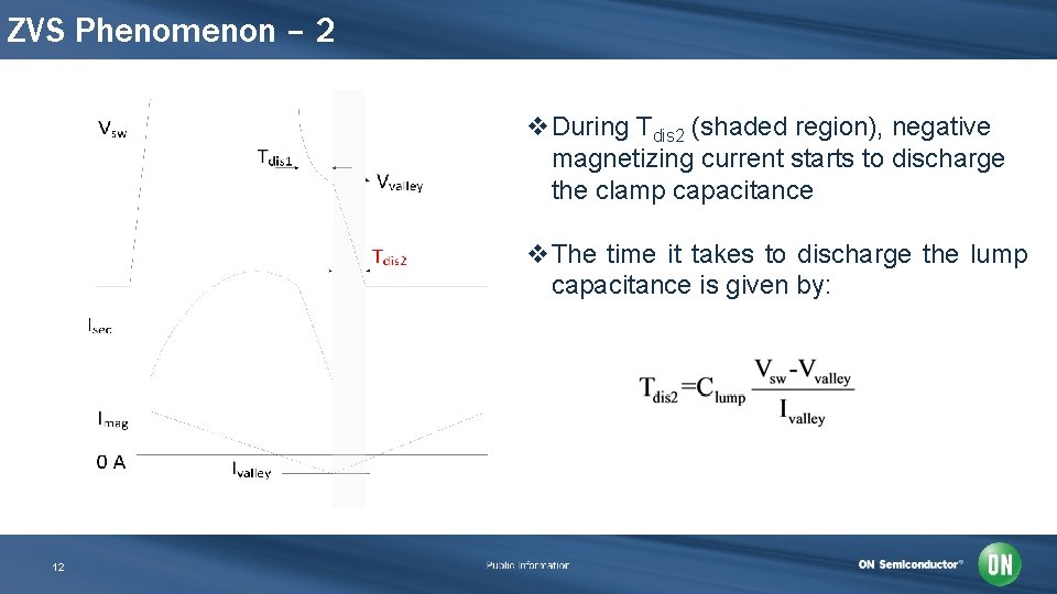
ZVS Phenomenon – 2 v. During Tdis 2 (shaded region), negative magnetizing current starts to discharge the clamp capacitance v. The time it takes to discharge the lump capacitance is given by: 12
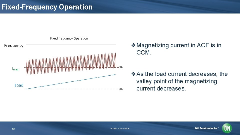
Fixed-Frequency Operation v. Magnetizing current in ACF is in CCM. v. As the load current decreases, the valley point of the magnetizing current decreases. 13
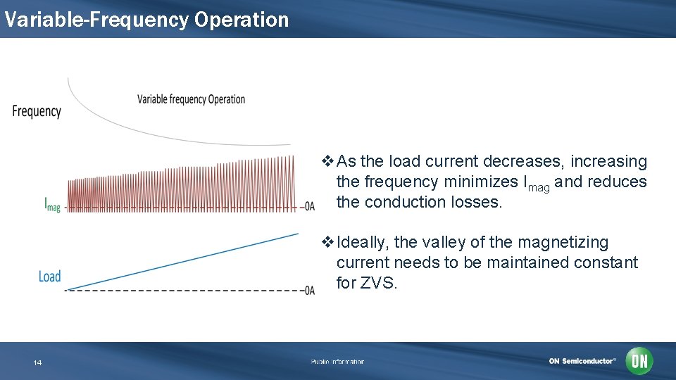
Variable-Frequency Operation v. As the load current decreases, increasing the frequency minimizes Imag and reduces the conduction losses. v. Ideally, the valley of the magnetizing current needs to be maintained constant for ZVS. 14
Light-Load Efficiency & Standby Power Challenge 15
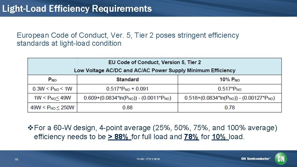
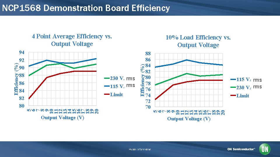
Light-Load Efficiency Requirements European Code of Conduct, Ver. 5, Tier 2 poses stringent efficiency standards at light-load condition v. For a 60 -W design, 4 -point average (25%, 50%, 75%, and 100% average) efficiency needs to be > 88% for full load and 78% for 10% load. 16
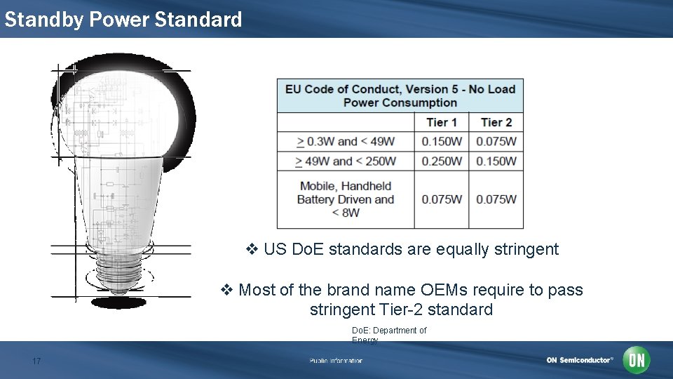
Standby Power Standard v US Do. E standards are equally stringent v Most of the brand name OEMs require to pass stringent Tier-2 standard Do. E: Department of Energy 17
ACF Specific Light-Load Challenges v. Magnetizing current is in CCM. v. Frequency modulation results in high-frequency operation at light load v. Classical frequency foldback is not possible to implement when magnetizing current is in CCM 18
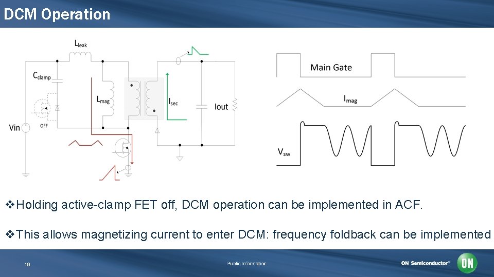
DCM Operation v. Holding active-clamp FET off, DCM operation can be implemented in ACF. v. This allows magnetizing current to enter DCM: frequency foldback can be implemented 19
Introduction to NCP 1568 Ac-Dc PWM Controller for ACF 20
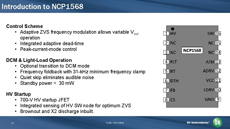
Introduction to NCP 1568 Control Scheme • Adaptive ZVS frequency modulation allows variable Vout operation • Integrated adaptive dead-time • Peak-current-mode control DCM & Light-Load Operation • Optional transition to DCM mode • Frequency foldback with 31 -k. Hz minimum frequency clamp • Quiet skip eliminates audible noise • Standby power < 30 m. W HV Startup • 700 -V HV startup JFET • Integrated sensing of HV SW node for optimum ZVS • Brownout and X 2 discharge inbuilt. 21
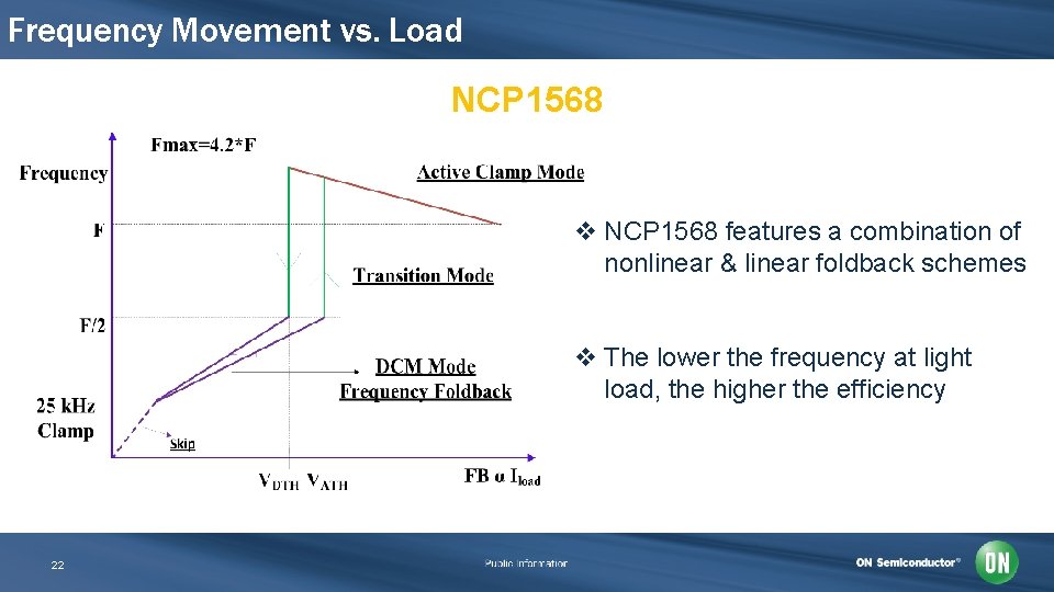
Frequency Movement vs. Load NCP 1568 v NCP 1568 features a combination of nonlinear & linear foldback schemes v The lower the frequency at light load, the higher the efficiency 22
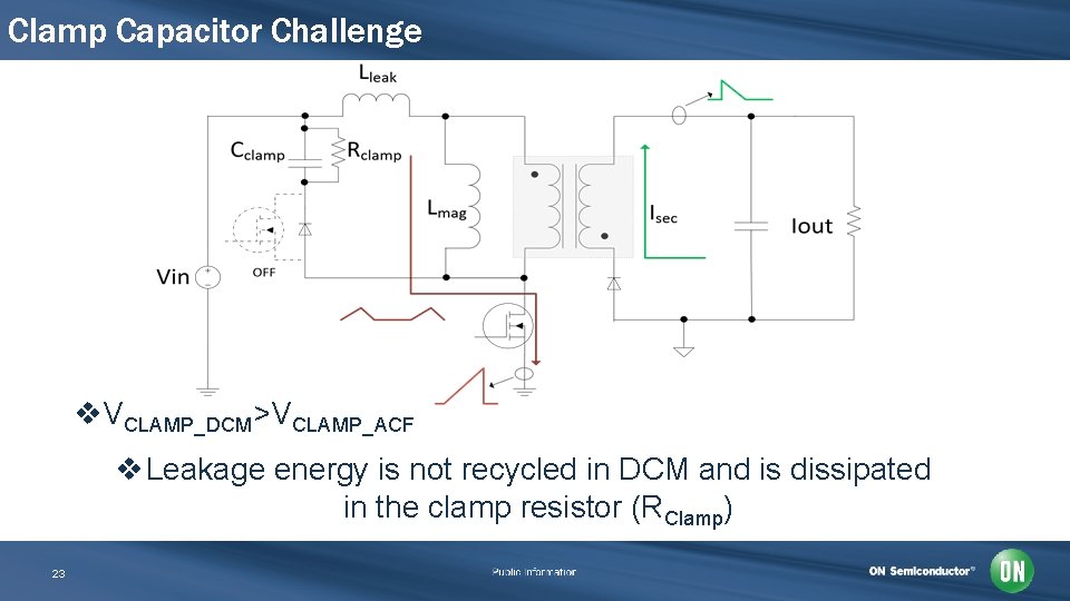
Clamp Capacitor Challenge v. VCLAMP_DCM>VCLAMP_ACF v Leakage energy is not recycled in DCM and is dissipated in the clamp resistor (RClamp) 23
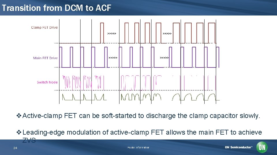
Transition from DCM to ACF v. Active-clamp FET can be soft-started to discharge the clamp capacitor slowly. v. Leading-edge modulation of active-clamp FET allows the main FET to achieve ZVS 24
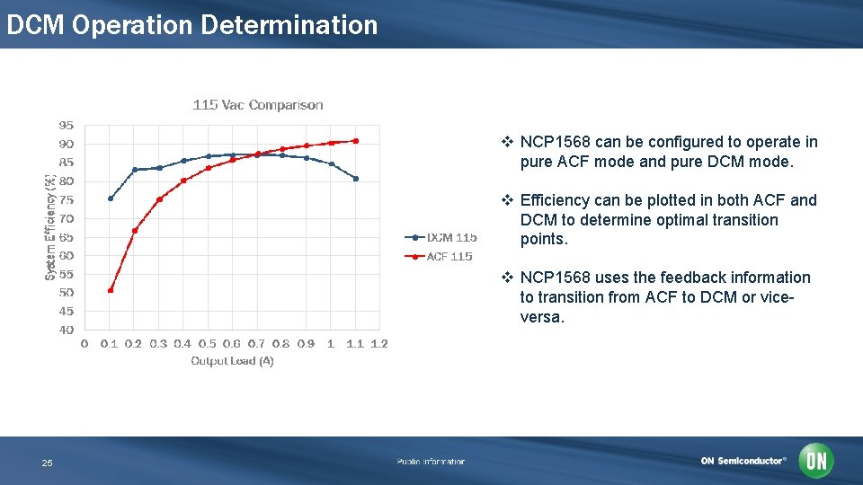
DCM Operation Determination v NCP 1568 can be configured to operate in pure ACF mode and pure DCM mode. v Efficiency can be plotted in both ACF and DCM to determine optimal transition points. v NCP 1568 uses the feedback information to transition from ACF to DCM or viceversa. 25
Key Components Selection Transformer Design & Key Equations 26
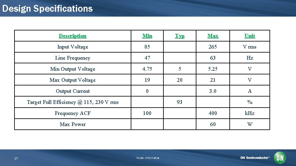
Design Specifications 27 Description Min Typ Max Unit Input Voltage 85 265 V rms Line Frequency 47 63 Hz Min Output Voltage 4. 75 5 5. 25 V Max Output Voltage 19 20 21 V Output Current 0 3. 0 A Target Full Efficiency @ 115, 230 V rms 93 % Frequency ACF 100 400 k. Hz Max Power 60 W
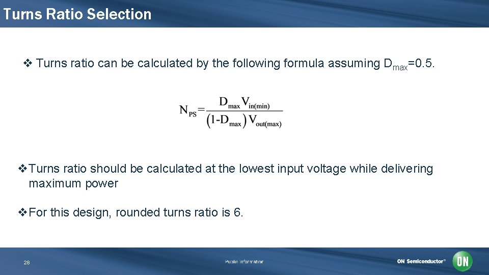
Turns Ratio Selection v Turns ratio can be calculated by the following formula assuming Dmax=0. 5. v. Turns ratio should be calculated at the lowest input voltage while delivering maximum power v. For this design, rounded turns ratio is 6. 28
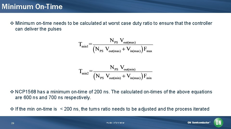
Minimum On-Time v Minimum on-time needs to be calculated at worst case duty ratio to ensure that the controller can deliver the pulses v NCP 1568 has a minimum on-time of 200 ns. The calculated on-times of the above equations are 600 ns and 700 ns respectively. v If the min on-time is < 200 ns, the turns ratio needs to be adjusted and the process iterated 29
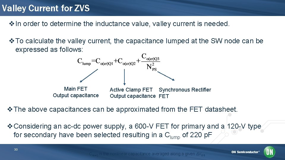
Valley Current for ZVS v. In order to determine the inductance value, valley current is needed. v. To calculate the valley current, the capacitance lumped at the SW node can be expressed as follows: Main FET Output capacitance Active Clamp FET Synchronous Rectifier Output capacitance FET v. The above capacitances can be approximated from the FET datasheet. v. Considering an ac-dc power supply, a 600 -V FET for primary and a 120 -V type for secondary have been selected resulting in a Clump of 220 p. F 30 Co(er) is the nonlinear capacitance averaged along a given VDS
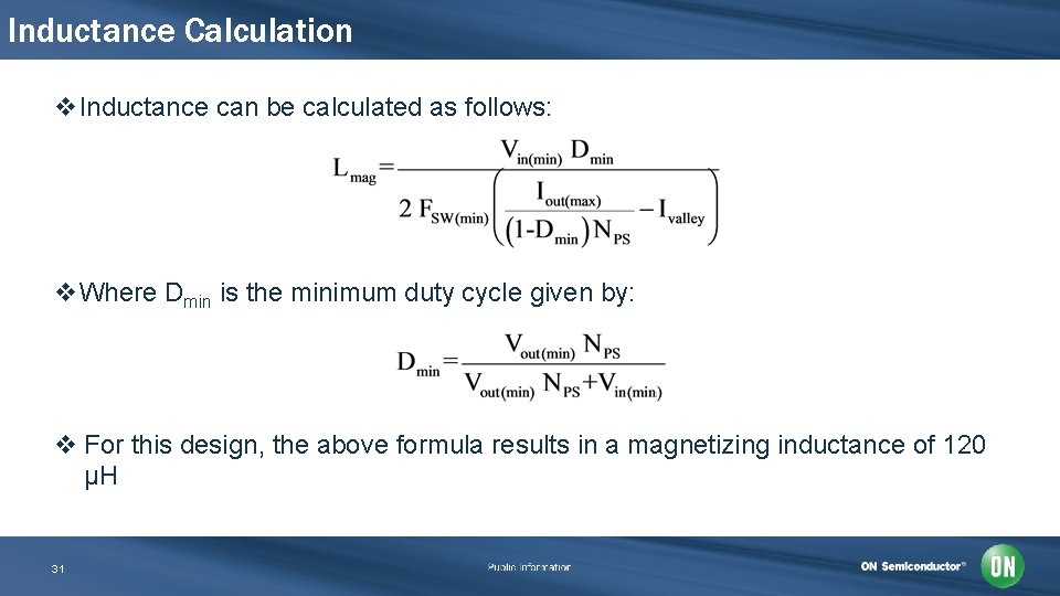
Inductance Calculation v. Inductance can be calculated as follows: v. Where Dmin is the minimum duty cycle given by: v For this design, the above formula results in a magnetizing inductance of 120 µH 31
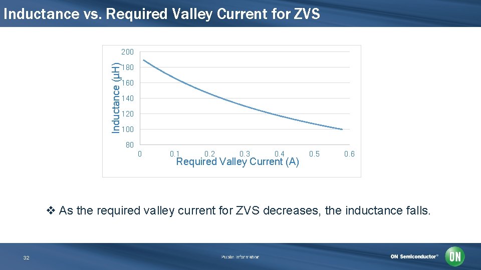
Inductance vs. Required Valley Current for ZVS Inductance (µH) 200 180 160 140 120 100 80 0 0. 1 0. 2 0. 3 0. 4 Required Valley Current (A) 0. 5 0. 6 v As the required valley current for ZVS decreases, the inductance falls. 32
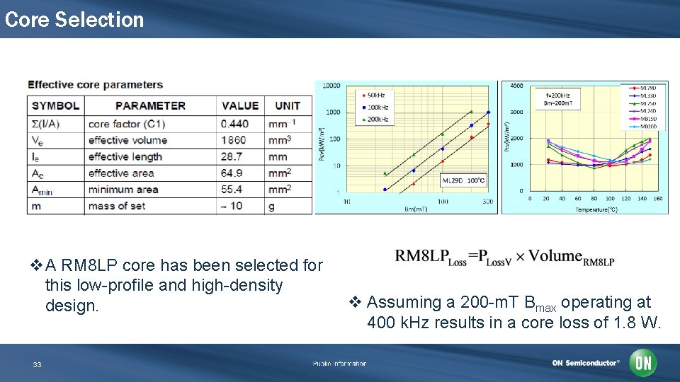
Core Selection v. A RM 8 LP core has been selected for this low-profile and high-density design. 33 v Assuming a 200 -m. T Bmax operating at 400 k. Hz results in a core loss of 1. 8 W.
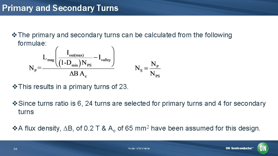
Primary and Secondary Turns v. The primary and secondary turns can be calculated from the following formulae: v. This results in a primary turns of 23. v. Since turns ratio is 6, 24 turns are selected for primary turns and 4 for secondary turns v. A flux density, ∆B, of 0. 2 T & Ae of 65 mm 2 have been assumed for this design. 34
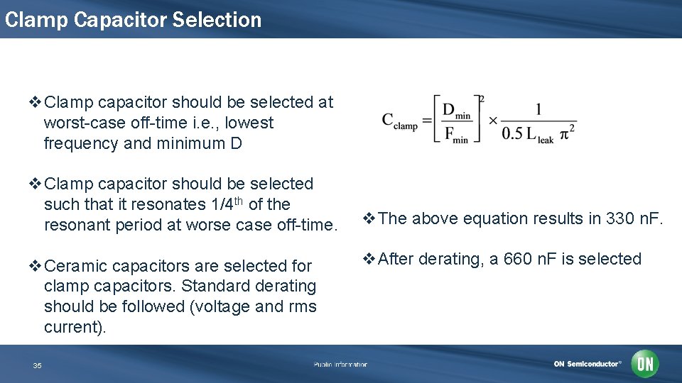
Clamp Capacitor Selection v. Clamp capacitor should be selected at worst-case off-time i. e. , lowest frequency and minimum D v. Clamp capacitor should be selected such that it resonates 1/4 th of the resonant period at worse case off-time. v. Ceramic capacitors are selected for clamp capacitors. Standard derating should be followed (voltage and rms current). 35 v. The above equation results in 330 n. F. v. After derating, a 660 n. F is selected
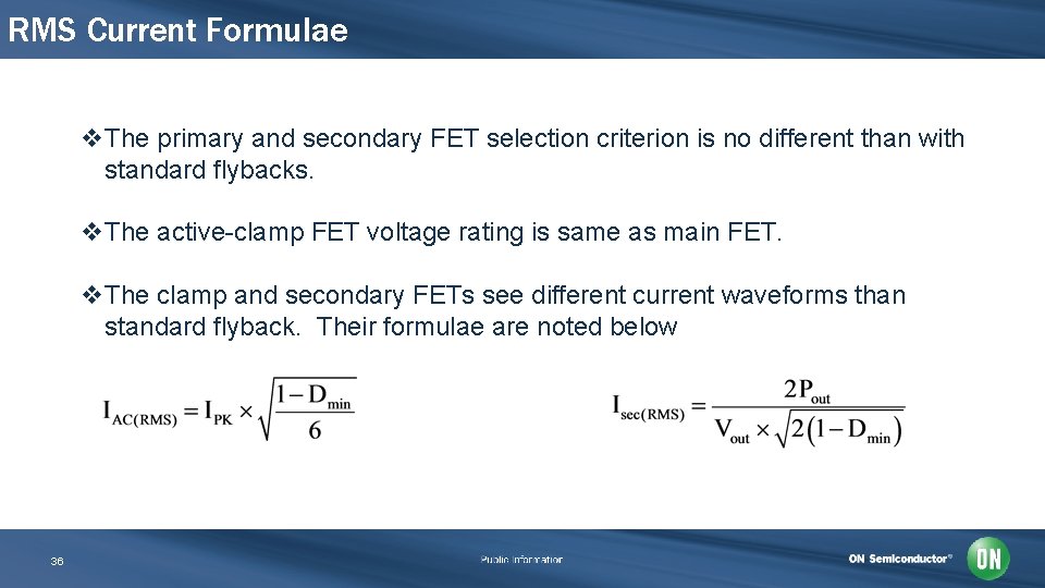
RMS Current Formulae v. The primary and secondary FET selection criterion is no different than with standard flybacks. v. The active-clamp FET voltage rating is same as main FET. v. The clamp and secondary FETs see different current waveforms than standard flyback. Their formulae are noted below 36
60 -W UHD-Board Performance 37
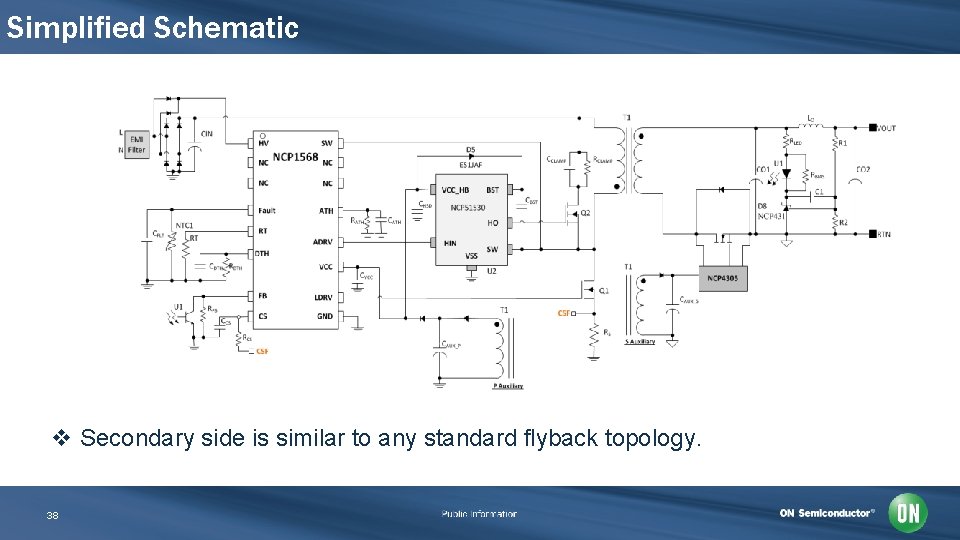
Simplified Schematic v Secondary side is similar to any standard flyback topology. 38
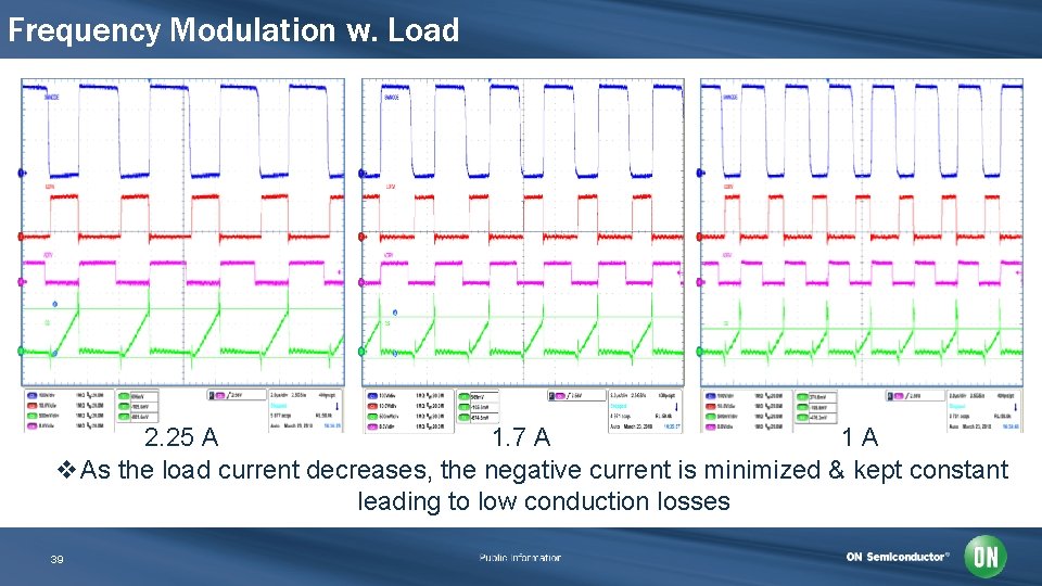
Frequency Modulation w. Load 1 A 2. 25 A 1. 7 A v. As the load current decreases, the negative current is minimized & kept constant leading to low conduction losses 39
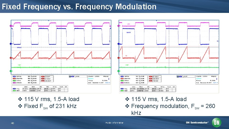
Fixed Frequency vs. Frequency Modulation v 115 V rms, 1. 5 -A load v Fixed Fsw of 231 k. Hz 40 v 115 V rms, 1. 5 -A load v Frequency modulation, Fsw = 260 k. Hz
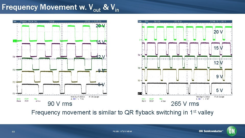
Frequency Movement w. Vout & Vin 20 V 15 V 12 V 9 V 9 V 5 V 5 V 265 V rms 90 V rms Frequency movement is similar to QR flyback switching in 1 st valley 41
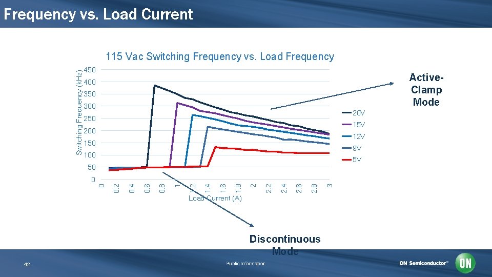
Frequency vs. Load Current Switching Frequency (k. Hz) 115 Vac Switching Frequency vs. Load Frequency 450 Active. Clamp Mode 400 350 300 20 V 250 15 V 200 12 V 150 9 V 100 5 V Load Current (A) Discontinuous Mode 42 3 2. 8 2. 6 2. 4 2. 2 2 1. 8 1. 6 1. 4 1. 2 1 0. 8 0. 6 0. 4 0. 2 0 0 50
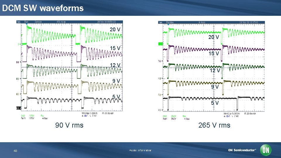
DCM SW waveforms 20 V 15 V 12 V 9 V 5 V 5 V 90 V rms 43 265 V rms
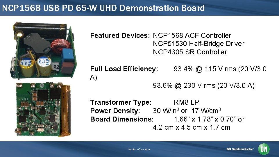
NCP 1568 USB PD 65 -W UHD Demonstration Board Featured Devices: NCP 1568 ACF Controller NCP 51530 Half-Bridge Driver NCP 4305 SR Controller Full Load Efficiency: 93. 4% @ 115 V rms (20 V/3. 0 A) 93. 6% @ 230 V rms (20 V/3. 0 A) Transformer Type: RM 8 LP Power Density: 30 W/in 3 or 17 W/cm 3 Board Dimensions: 1. 66” x 1. 78” x 0. 70” or 4. 2 cm x 4. 5 cm x 1. 7 cm
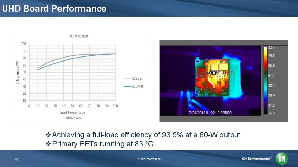
UHD Board Performance v. Achieving a full-load efficiency of 93. 5% at a 60 -W output v. Primary FETs running at 83 C 45
NCP 1568 Demonstration Board Efficiency Limit Output Voltage (V) 88 86 84 82 80 78 76 74 72 70 115 VAC rms 230 VAC Limit 5 6 7 8 9 10 11 12 13 14 15 16 17 18 19 20 230 VAC rms 115 VAC 10% Load Efficiency vs. Output Voltage Efficiency (%) 94 92 90 88 86 84 82 80 5 6 7 8 9 10 11 12 13 14 15 16 17 18 19 20 Efficiency (%) 4 Point Average Efficiency vs. Output Voltage (V)
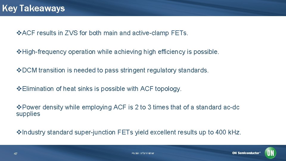
Key Takeaways v. ACF results in ZVS for both main and active-clamp FETs. v. High-frequency operation while achieving high efficiency is possible. v. DCM transition is needed to pass stringent regulatory standards. v. Elimination of heat sinks is possible with ACF topology. v. Power density while employing ACF is 2 to 3 times that of a standard ac-dc supplies v. Industry standard super-junction FETs yield excellent results up to 400 k. Hz. 47
- Slides: 47