HIGH SPEED ELECTRICAL TRANSMISSION LINE DESIGN AND CHARACTERISATION
![d. B SIMULATIONS f [10 GHz] • Linear distributions (acausal), low transmission loss (few d. B SIMULATIONS f [10 GHz] • Linear distributions (acausal), low transmission loss (few](https://slidetodoc.com/presentation_image_h/b60a4131acdf5f4d22135e0ee7d6ac59/image-21.jpg)
![SIMULATIONS d. B DIFFERENT CONDUCTOR RADIUS COMPARAISON f [10 GHz] Larger radius gives better SIMULATIONS d. B DIFFERENT CONDUCTOR RADIUS COMPARAISON f [10 GHz] Larger radius gives better](https://slidetodoc.com/presentation_image_h/b60a4131acdf5f4d22135e0ee7d6ac59/image-37.jpg)
- Slides: 38

HIGH SPEED ELECTRICAL TRANSMISSION LINE DESIGN AND CHARACTERISATION TWEPP 2016 Leyre Flores, Richard Bates, Craig Buttar, Jan Buytaert, Lars Eklund, Iain Longstaff, Sneha Naik, Stephanie Sullivan, Kenneth Wraight

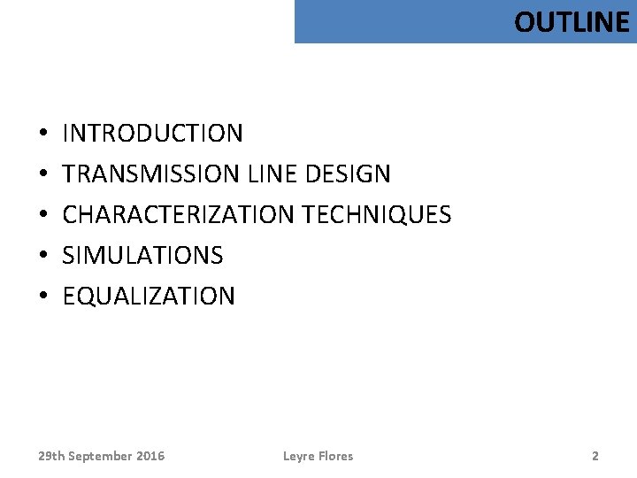
OUTLINE • • • INTRODUCTION TRANSMISSION LINE DESIGN CHARACTERIZATION TECHNIQUES SIMULATIONS EQUALIZATION 29 th September 2016 Leyre Flores 2

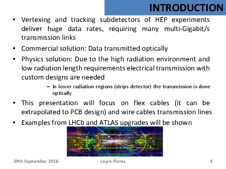
INTRODUCTION • Vertexing and tracking subdetectors of HEP experiments deliver huge data rates, requiring many multi-Gigabit/s transmission links • Commercial solution: Data transmitted optically • Physics solution: Due to the high radiation environment and low radiation length requirements electrical transmission with custom designs are needed – In lower radiation regions (strips detector) the transmission is done optically • This presentation will focus on flex cables (it can be extrapolated to PCB design) and wire cables transmission lines • Examples from LHCb and ATLAS upgrades will be shown 29 th September 2016 Leyre Flores 3

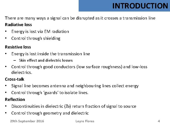
INTRODUCTION There are many ways a signal can be disrupted as it crosses a transmission line Radiative loss • Energy is lost via EM radiation • Control through shielding Resistive loss • Energy is lost inside the transmission line – Skin effect and dielectric losses • Control through good conductors (low surface roughness) and low-loss dielectrics. Cross-talk • Signal line becomes antenna and neighbouring lines collect energy • Control through ‘guards’ to isolate lines. Reflection • Discontinuities in dielectric (Z 0) return fraction of signal to source • Control through geometry and dielectric 29 th September 2016 Leyre Flores 4

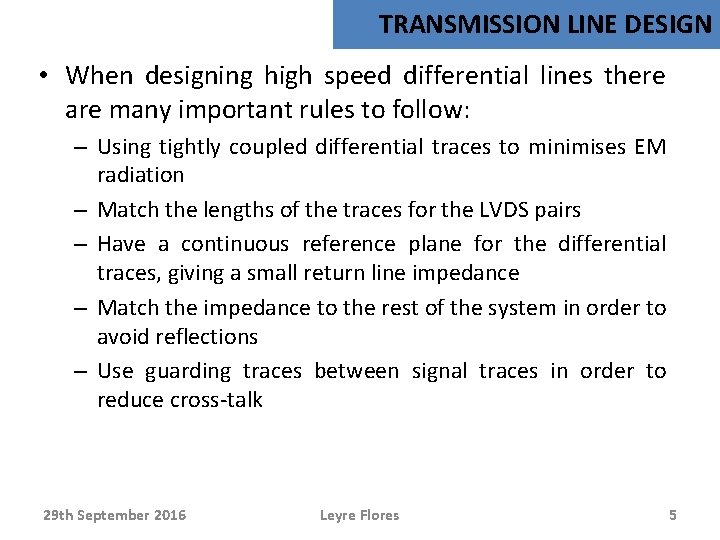
TRANSMISSION LINE DESIGN • When designing high speed differential lines there are many important rules to follow: – Using tightly coupled differential traces to minimises EM radiation – Match the lengths of the traces for the LVDS pairs – Have a continuous reference plane for the differential traces, giving a small return line impedance – Match the impedance to the rest of the system in order to avoid reflections – Use guarding traces between signal traces in order to reduce cross-talk 29 th September 2016 Leyre Flores 5

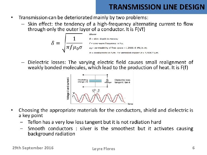
TRANSMISSION LINE DESIGN • 29 th September 2016 Leyre Flores 6

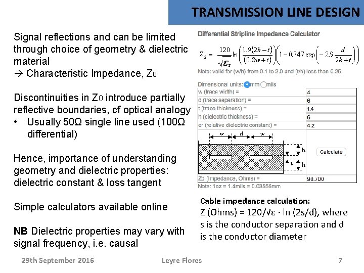
TRANSMISSION LINE DESIGN Signal reflections and can be limited through choice of geometry & dielectric material Characteristic Impedance, Z 0 Discontinuities in Z 0 introduce partially reflective boundaries, cf optical analogy • Usually 50Ω single line used (100Ω differential) Hence, importance of understanding geometry and dielectric properties: dielectric constant & loss tangent Simple calculators available online NB Dielectric properties may vary with signal frequency, i. e. causal 29 th September 2016 Cable impedance calculation: Z (Ohms) = 120/√ε · ln (2 s/d), where s is the conductor separation and d is the conductor diameter Leyre Flores 7

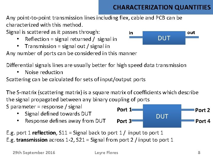
CHARACTERIZATION QUANTITIES Any point-to-point transmission lines including flex, cable and PCB can be characterized with this method. Signal is scattered as it passes through: out in DUT • Reflection = signal returned / signal in • Transmission = signal out / signal in Any number of ports can be considered in this manner Differential signals lines are usually better for high speed data transmission • Noise reduction Scattering can be calculated for sets of input/output ports The S-matrix (scattering matrix) is a square matrix of coefficients which describe the signal propagated between any binary coupling of ports S parameter = response / signal Port 1 Port 2 • Signal defined towards DUT • Response defines away from DUT Port 4 Port 3 E. g. port 1 reflection, S 11 = Signal back to port 1 / input to port 1 E. g. transmission across 1 -2, S 21 = Signal from port 2 / input to port 1 29 th September 2016 Leyre Flores 8

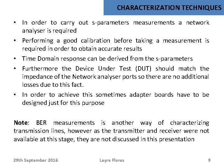
CHARACTERIZATION TECHNIQUES • In order to carry out s-parameters measurements a network analyser is required • Performing a good calibration before taking a measurement is required in order to obtain accurate results • Time Domain response can be derived from the s-parameters • Furthermore the Device Under Test (DUT) should match the impedance of the Network analyser ports so there are no additional losses due to this fact. • In order to achieve this sometimes adapter boards have to be designed just for this purpose Note: BER measurements is another way of characterizing transmission lines, however as the transmitter and receiver were not available at this stage, they are not discussed in this presentation 29 th September 2016 Leyre Flores 9

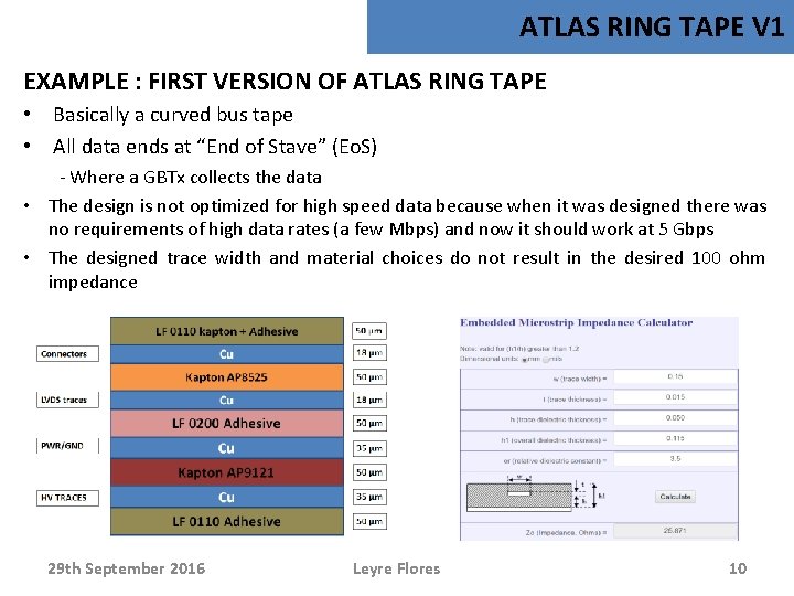
ATLAS RING TAPE V 1 EXAMPLE : FIRST VERSION OF ATLAS RING TAPE • Basically a curved bus tape • All data ends at “End of Stave” (Eo. S) - Where a GBTx collects the data • The design is not optimized for high speed data because when it was designed there was no requirements of high data rates (a few Mbps) and now it should work at 5 Gbps • The designed trace width and material choices do not result in the desired 100 ohm impedance 29 th September 2016 Leyre Flores 10

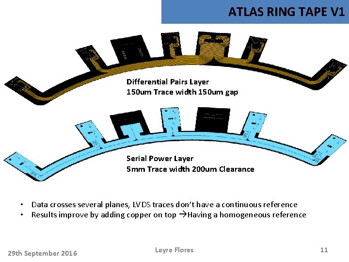
ATLAS RING TAPE V 1 Differential Pairs Layer 150 um Trace width 150 um gap Serial Power Layer 5 mm Trace width 200 um Clearance • Data crosses several planes, LVDS traces don’t have a continuous reference • Results improve by adding copper on top Having a homogeneous reference 29 th September 2016 Leyre Flores 11

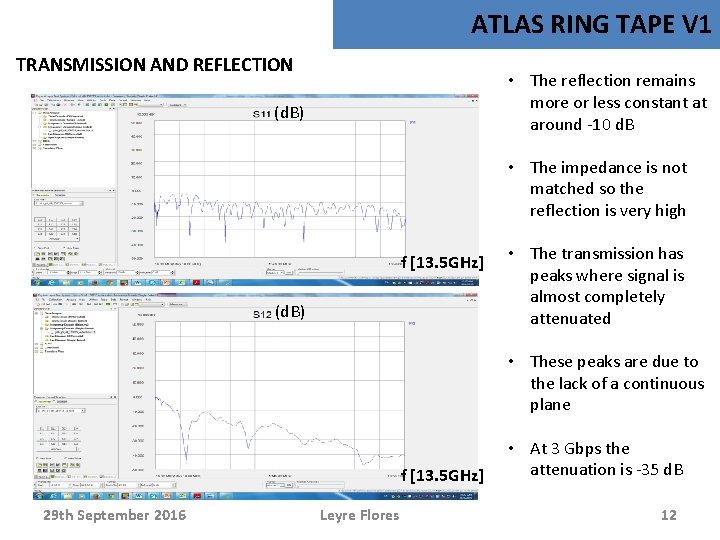
ATLAS RING TAPE V 1 TRANSMISSION AND REFLECTION • The reflection remains more or less constant at around -10 d. B (d. B) • The impedance is not matched so the reflection is very high f [13. 5 GHz] (d. B) • The transmission has peaks where signal is almost completely attenuated • These peaks are due to the lack of a continuous plane f [13. 5 GHz] 29 th September 2016 Leyre Flores • At 3 Gbps the attenuation is -35 d. B 12

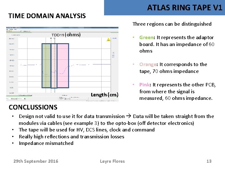
ATLAS RING TAPE V 1 TIME DOMAIN ANALYSIS Three regions can be distinguished (ohms) • Green: It represents the adaptor board. It has an impedance of 60 ohms • Orange: It corresponds to the tape, 70 ohms impedance Length (cm) • Pink: It represents the other PCB, from where the signal is measured, 60 ohms impedance. CONCLUSSIONS • Design not valid to use it for data transmission Data will be taken straight from the modules via cables (see example 3) to the opto-box (off detector electronics) • The tape will be used for HV, DCS lines, clock and command • Really high reflections and transmission losses • Impedance mismatched 29 th September 2016 Leyre Flores 13

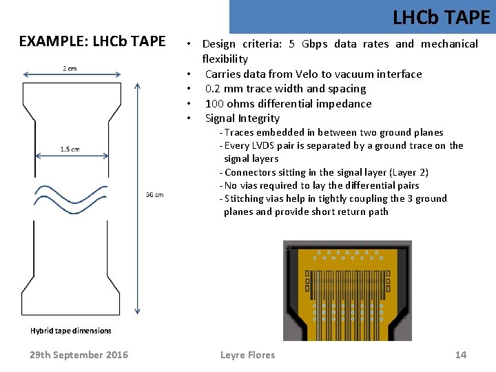
LHCb TAPE EXAMPLE: LHCb TAPE • Design criteria: 5 Gbps data rates and mechanical flexibility • Carries data from Velo to vacuum interface • 0. 2 mm trace width and spacing • 100 ohms differential impedance • Signal Integrity - Traces embedded in between two ground planes - Every LVDS pair is separated by a ground trace on the signal layers - Connectors sitting in the signal layer (Layer 2) - No vias required to lay the differential pairs - Stitching vias help in tightly coupling the 3 ground planes and provide short return path Hybrid tape dimensions 29 th September 2016 Leyre Flores 14

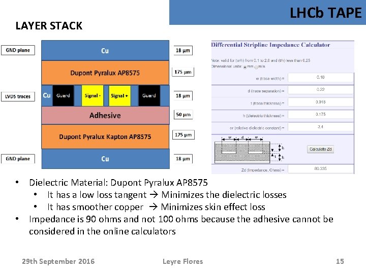
LHCb TAPE LAYER STACK • Dielectric Material: Dupont Pyralux AP 8575 • It has a low loss tangent Minimizes the dielectric losses • It has smoother copper Minimizes skin effect loss • Impedance is 90 ohms and not 100 ohms because the adhesive cannot be considered in the online calculators 29 th September 2016 Leyre Flores 15

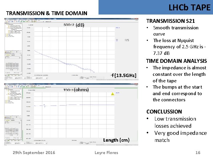
LHCb TAPE TRANSMISSION & TIME DOMAIN TRANSMISSION S 21 (d. B) • Smooth transmission curve • The loss at Nyquist frequency of 2. 5 GHz is 7. 37 d. B TIME DOMAIN ANALYSIS f [13. 5 GHz] (ohms) Length (cm) 29 th September 2016 Leyre Flores • The impedance is almost constant over the length of the tape • The bumps at the start and end correspond to the connectors CONCLUSSION • Low transmission losses achieved • Very good impedance match 16

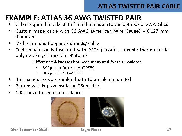
ATLAS TWISTED PAIR CABLE EXAMPLE: ATLAS 36 AWG TWISTED PAIR • Cable required to take data from the module to the optobox at 2. 5 -5 Gbps • Custom made cable with 36 AWG (American Wire Gauge) ≈ 0. 127 mm diameter • Multi-stranded Copper : 7 strands/ cable • Each conductor is insulated with PEEK (colorless organic thermoplastic polymer, Poly-Ether-Ketone) - Different thicknesses has been measured for this insulator • • 390 µm for “transparent” PEEK 307 µm for “blue” PEEK • Both conductors are shielded with 10 μm aluminium foil • Backed with kapton insulator, 25 um thick • 100 ohm differential impedance 29 th September 2016 Leyre Flores 17

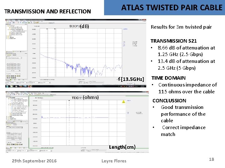
TRANSMISSION AND REFLECTION ATLAS TWISTED PAIR CABLE (d. B) Results for 3 m twisted pair TRANSMISSION S 21 • 8. 66 d. B of attenuation at 1. 25 GHz (2. 5 Gbps) • 13. 4 d. B of attenuation at 2. 5 GHz (5 Gbps) f [13. 5 GHz] (ohms) TIME DOMAIN • Continuous impedance of 115 ohms over the cable CONCLUSSION • Good transmission performance of the cable • Correct impedance match Length(cm) 29 th September 2016 Leyre Flores 18

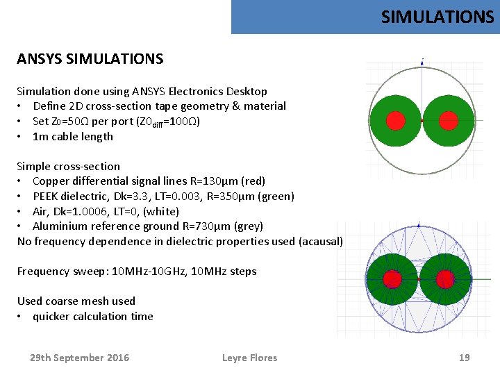
SIMULATIONS ANSYS SIMULATIONS Simulation done using ANSYS Electronics Desktop • Define 2 D cross-section tape geometry & material • Set Z 0=50Ω per port (Z 0 diff=100Ω) • 1 m cable length Simple cross-section • Copper differential signal lines R=130µm (red) • PEEK dielectric, Dk=3. 3, LT=0. 003, R=350µm (green) • Air, Dk=1. 0006, LT=0, (white) • Aluminium reference ground R=730µm (grey) No frequency dependence in dielectric properties used (acausal) Frequency sweep: 10 MHz-10 GHz, 10 MHz steps Used coarse mesh used • quicker calculation time 29 th September 2016 Leyre Flores 19

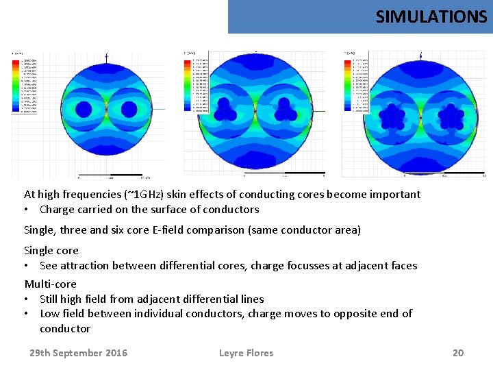
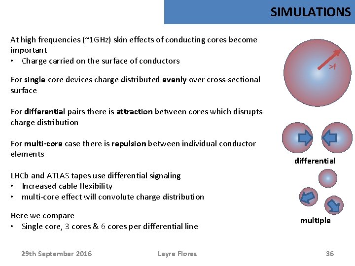
SIMULATIONS At high frequencies (~1 GHz) skin effects of conducting cores become important • Charge carried on the surface of conductors Single, three and six core E-field comparison (same conductor area) Single core • See attraction between differential cores, charge focusses at adjacent faces Multi-core • Still high field from adjacent differential lines • Low field between individual conductors, charge moves to opposite end of conductor 29 th September 2016 Leyre Flores 20
![d B SIMULATIONS f 10 GHz Linear distributions acausal low transmission loss few d. B SIMULATIONS f [10 GHz] • Linear distributions (acausal), low transmission loss (few](https://slidetodoc.com/presentation_image_h/b60a4131acdf5f4d22135e0ee7d6ac59/image-21.jpg)
d. B SIMULATIONS f [10 GHz] • Linear distributions (acausal), low transmission loss (few d. B) over range • Little comparative effect seen on reflection and transmission between core variations • For the same cross-sectional area ( same mass ) multiple conductors per core offer a flexible alternative to single core tapes • Transmission favoured by large conductor radius 29 th September 2016 Leyre Flores 21

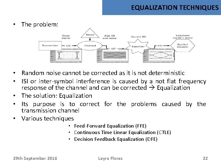
EQUALIZATION TECHNIQUES • The problem: • Random noise cannot be corrected as it is not deterministic • ISI or inter-symbol interference is caused by a not flat frequency response of the channel and can be corrected Equalization • The solution: Equalization • Its purpose is to correct for the problems caused by the transmission channel • Various techniques • Feed-Forward Equalization (FFE) • Continuous Time Linear Equalization (CTLE) • Decision Feedback Equalization (DFE) 29 th September 2016 Leyre Flores 22

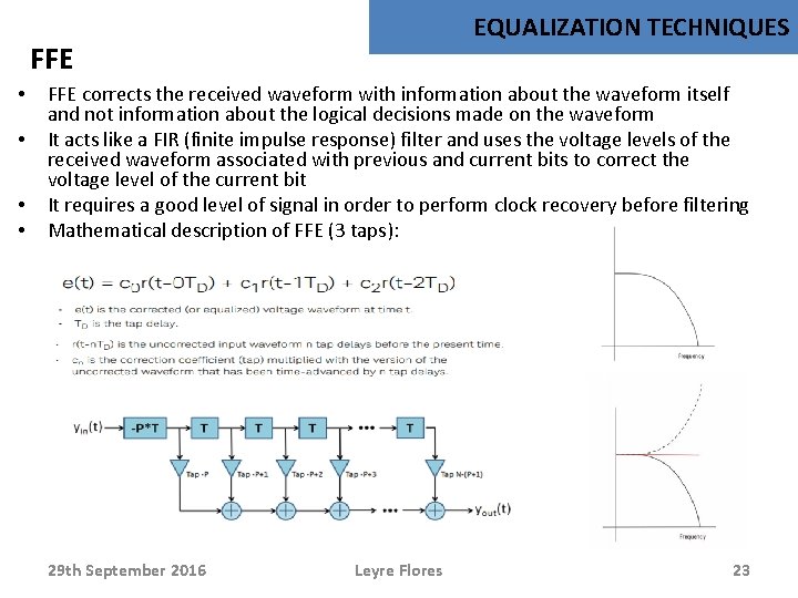
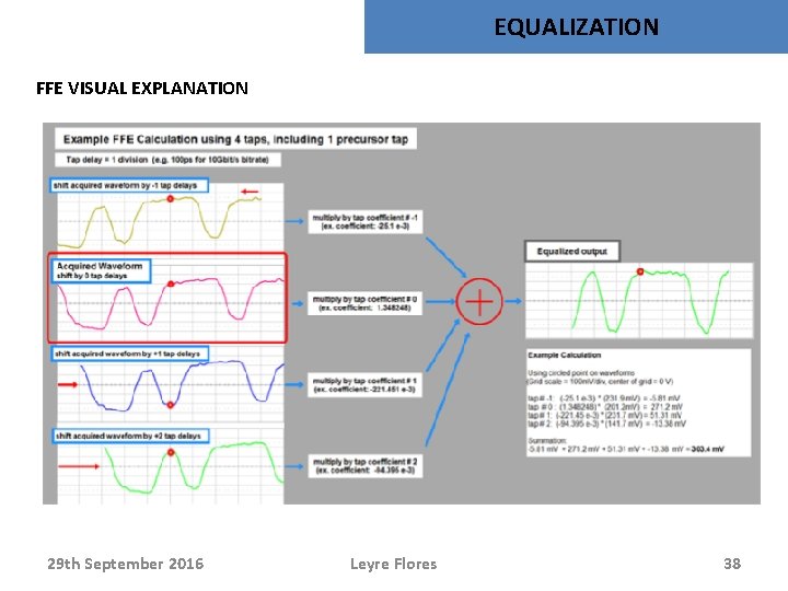
EQUALIZATION TECHNIQUES FFE • • FFE corrects the received waveform with information about the waveform itself and not information about the logical decisions made on the waveform It acts like a FIR (finite impulse response) filter and uses the voltage levels of the received waveform associated with previous and current bits to correct the voltage level of the current bit It requires a good level of signal in order to perform clock recovery before filtering Mathematical description of FFE (3 taps): 29 th September 2016 Leyre Flores 23

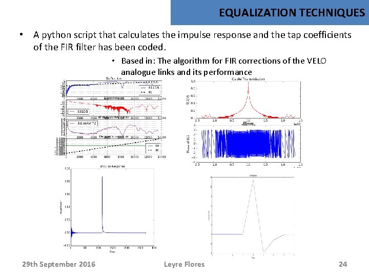
EQUALIZATION TECHNIQUES • A python script that calculates the impulse response and the tap coefficients of the FIR filter has been coded. • Based in: The algorithm for FIR corrections of the VELO analogue links and its performance 29 th September 2016 Leyre Flores 24

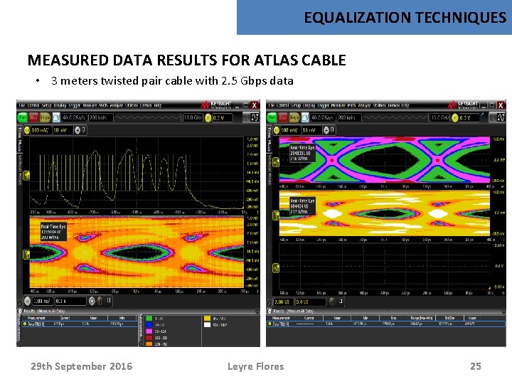
EQUALIZATION TECHNIQUES MEASURED DATA RESULTS FOR ATLAS CABLE • 3 meters twisted pair cable with 2. 5 Gbps data 29 th September 2016 Leyre Flores 25

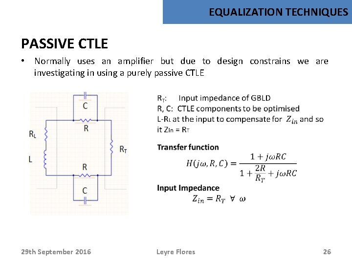
EQUALIZATION TECHNIQUES PASSIVE CTLE • Normally uses an amplifier but due to design constrains we are investigating in using a purely passive CTLE 29 th September 2016 Leyre Flores 26

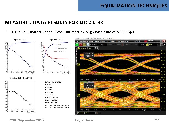
EQUALIZATION TECHNIQUES MEASURED DATA RESULTS FOR LHCb LINK • LHCb link: Hybrid + tape + vacuum feed-through with data at 5. 12 Gbps 29 th September 2016 Leyre Flores 27

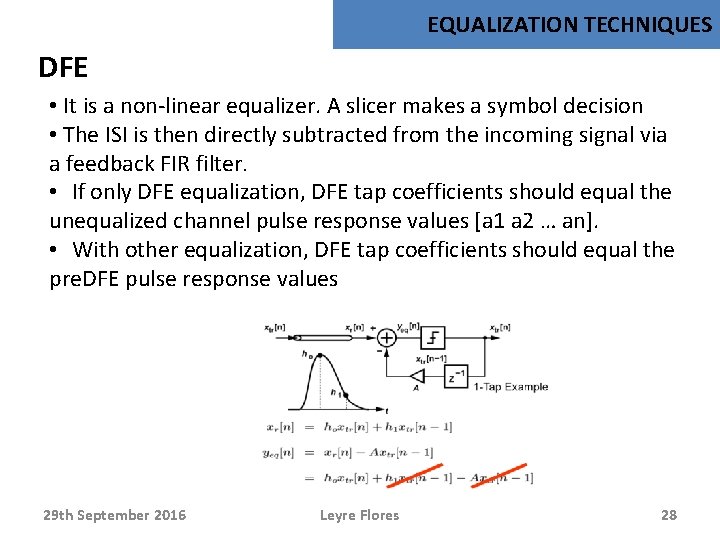
EQUALIZATION TECHNIQUES DFE • It is a non-linear equalizer. A slicer makes a symbol decision • The ISI is then directly subtracted from the incoming signal via a feedback FIR filter. • If only DFE equalization, DFE tap coefficients should equal the unequalized channel pulse response values [a 1 a 2 … an]. • With other equalization, DFE tap coefficients should equal the pre. DFE pulse response values 29 th September 2016 Leyre Flores 28

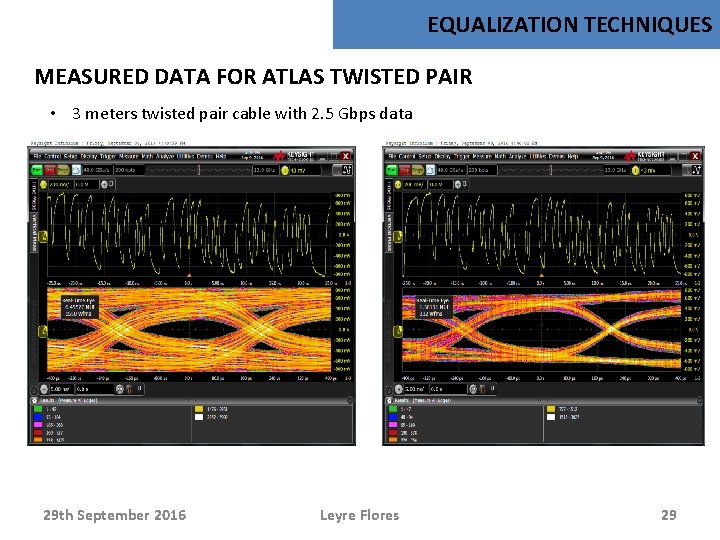
EQUALIZATION TECHNIQUES MEASURED DATA FOR ATLAS TWISTED PAIR • 3 meters twisted pair cable with 2. 5 Gbps data 29 th September 2016 Leyre Flores 29

CONCLUSION • Transmission lines at high speed require a very careful design – Parameters to consider while designing a transmission line: • Material choice In order to avoid skin effect and dielectric losses as well as matching the impedance • Geometry of the design PCBs (stripline, microstrip etc. ) or cable • Recovering performance Equalization techniques • In order to be able to fully characterize a transmission line in the measurements should be included the whole chain: transmitter + channel (tapes and cables) + receiver • Reducing the number of connectors improves the signal quality as there are less reflections due to impedance mismatches • Very difficult to design a transmission line with low material requirements (High Energy Physics experiments) • Final tests will be BER measurements with transmitter and receivers will be performed 29 th September 2016 Leyre Flores 30

THANK YOU 29 th September 2016 Leyre Flores 31

BACK-UP 29 th September 2016 Leyre Flores 32

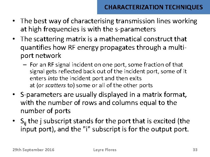
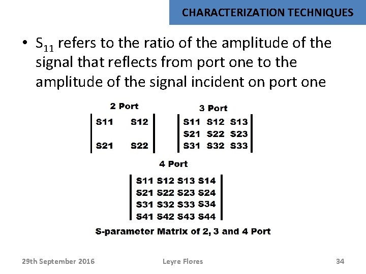
CHARACTERIZATION TECHNIQUES • The best way of characterising transmission lines working at high frequencies is with the s-parameters • The scattering matrix is a mathematical construct that quantifies how RF energy propagates through a multiport network – For an RF signal incident on one port, some fraction of that signal gets reflected back out of the incident port, some of it enters into the incident port and then exits at (or scatters to) some or all of the other ports • S-parameters are usually displayed in a matrix format, with the number of rows and columns equal to the number of ports • Sij the j subscript stands for the port that is excited (the input port), and the "i" subscript is for the output port. 29 th September 2016 Leyre Flores 33

CHARACTERIZATION TECHNIQUES • S 11 refers to the ratio of the amplitude of the signal that reflects from port one to the amplitude of the signal incident on port one 29 th September 2016 Leyre Flores 34

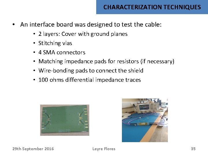
CHARACTERIZATION TECHNIQUES • An interface board was designed to test the cable: • • • 2 layers: Cover with ground planes Stitching vias 4 SMA connectors Matching impedance pads for resistors (if necessary) Wire-bonding pads to connect the shield 100 ohms differential impedance traces 29 th September 2016 Leyre Flores 35

SIMULATIONS At high frequencies (~1 GHz) skin effects of conducting cores become important • Charge carried on the surface of conductors >f For single core devices charge distributed evenly over cross-sectional surface For differential pairs there is attraction between cores which disrupts charge distribution For multi-core case there is repulsion between individual conductor elements differential LHCb and ATLAS tapes use differential signaling • Increased cable flexibility • multi-core effect will convolute charge distribution Here we compare • Single core, 3 cores & 6 cores per differential line 29 th September 2016 Leyre Flores multiple 36
![SIMULATIONS d B DIFFERENT CONDUCTOR RADIUS COMPARAISON f 10 GHz Larger radius gives better SIMULATIONS d. B DIFFERENT CONDUCTOR RADIUS COMPARAISON f [10 GHz] Larger radius gives better](https://slidetodoc.com/presentation_image_h/b60a4131acdf5f4d22135e0ee7d6ac59/image-37.jpg)
SIMULATIONS d. B DIFFERENT CONDUCTOR RADIUS COMPARAISON f [10 GHz] Larger radius gives better transmission • More divergence seen at higher frequencies skin effect • Seems to be saturation R > 180µm Only conductor radius changed so geometry not adapted to Z 0 reflections 29 th September 2016 Leyre Flores 37

EQUALIZATION FFE VISUAL EXPLANATION 29 th September 2016 Leyre Flores 38