High Resolution Digital FlatPanel Xray Detector Based on

High Resolution Digital Flat-Panel X-ray Detector Based on Large Area CMOS Image Sensor Korea Electro-technology Research Institute Advanced Medical Device Research Center Chorong Kim, Bokyung Cha, Keedong Yang, ryunkyung Kim, Sungchae Jeon PIXEL 2014, Niagara Falls (Canada), 5 September 2014
Outline n Introduction n CMOS X-ray detector module n X-ray characteristics n Future works n Summary crkim@keri. re. kr 2
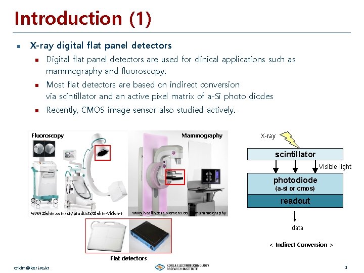
Introduction (1) n X-ray digital flat panel detectors n n n Digital flat panel detectors are used for clinical applications such as mammography and fluoroscopy. Most flat detectors are based on indirect conversion via scintillator and an active pixel matrix of a-Si photo diodes Recently, CMOS image sensor also studied actively. Fluoroscopy Mammography X-ray scintillator Visible light photodiode (a-si or cmos) readout www. ziehm. com/en/products/ziehm-vision-r www. healthcare. siemens. co. kr/mammography data < Indirect Conversion > Flat detectors crkim@keri. re. kr 3
Introduction (2) n Advantages of CMOS process for flat panel detector n CMOS process enables integration of many additional features. n On-pixel amplification n Various pixel circuits from 3 transistors(3 -TR) up to 100 transistors per pixel n n Electronic shutter n n Integrating detectors with CMOS readout circuits ( e. g. A/D conversion, Logic) global shutter, rolling shutter, non-destructive reads Overcome the size limitation through advanced process technology n No more problem with producing large area CMOS image sensor. ⇒ We study on a high resolution X-ray detector to acquire high quality images for real-time display based on CMOS sensor. crkim@keri. re. kr 4
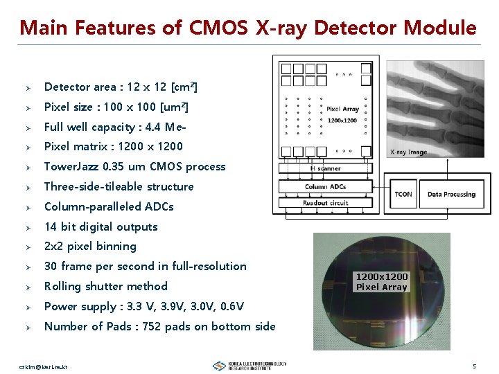
Main Features of CMOS X-ray Detector Module Ø Detector area : 12 x 12 [cm 2] Ø Pixel size : 100 x 100 [um 2] Ø Full well capacity : 4. 4 Me- Ø Pixel matrix : 1200 x 1200 Ø Tower. Jazz 0. 35 um CMOS process Ø Three-side-tileable structure Ø Column-paralleled ADCs Ø 14 bit digital outputs Ø 2 x 2 pixel binning Ø 30 frame per second in full-resolution Ø Rolling shutter method Ø Power supply : 3. 3 V, 3. 9 V, 3. 0 V, 0. 6 V Ø Number of Pads : 752 pads on bottom side crkim@keri. re. kr 1200 x 1200 Pixel Array 5
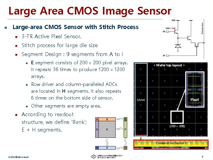
Large Area CMOS Image Sensor n Large-area CMOS Sensor with Stitch Process n 3 -TR Active Pixel Sensor. n Stitch process for large die size n Segment Design : 9 segments from A to I n n E segment consists of 200 x 200 pixel arrays. It repeats 36 times to produce 1200 x 1200 arrays. Row driver and column-paralleled ADCs are located in H segments. It also repeats 6 times on the bottom side of sensor. < Wafer top layout > Pixel BANK Other segments are empty area. According to readout structure, we define ‘Bank’; E + H segments. A B C D E F (200 x 200) < readout top layout > G crkim@keri. re. kr H I 6
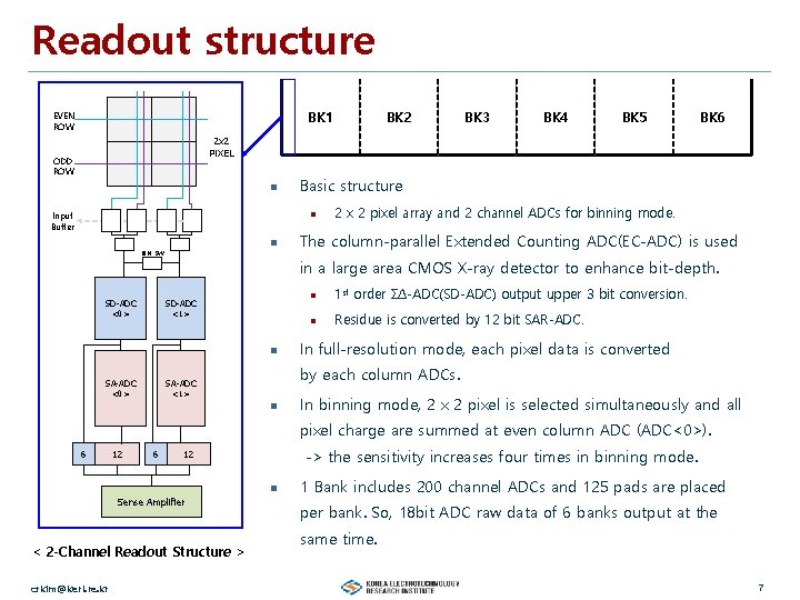
Readout structure BK 1 EVEN ROW BK 2 BK 3 BK 4 BK 5 BK 6 2 x 2 PIXEL ODD ROW n Input Buffer Basic structure n n BIN SW SD-ADC <0> The column-parallel Extended Counting ADC(EC-ADC) is used in a large area CMOS X-ray detector to enhance bit-depth. SD-ADC <1> n SA-ADC <0> 2 x 2 pixel array and 2 channel ADCs for binning mode. n 1 st order ΣΔ-ADC(SD-ADC) output upper 3 bit conversion. n Residue is converted by 12 bit SAR-ADC. In full-resolution mode, each pixel data is converted by each column ADCs. SA-ADC <1> n In binning mode, 2 x 2 pixel is selected simultaneously and all pixel charge are summed at even column ADC (ADC<0>). 6 12 6 -> the sensitivity increases four times in binning mode. 12 n Sense Amplifier < 2 -Channel Readout Structure > crkim@keri. re. kr 1 Bank includes 200 channel ADCs and 125 pads are placed per bank. So, 18 bit ADC raw data of 6 banks output at the same time. 7
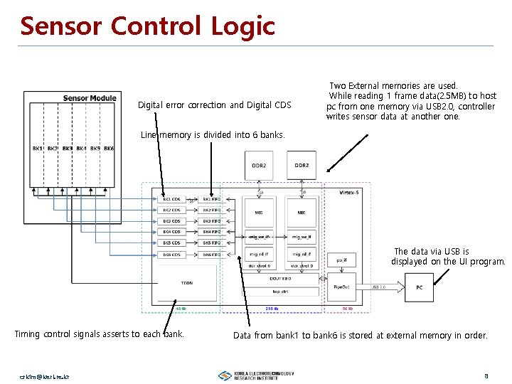
Sensor Control Logic Digital error correction and Digital CDS Two External memories are used. While reading 1 frame data(2. 5 MB) to host pc from one memory via USB 2. 0, controller writes sensor data at another one. Line memory is divided into 6 banks. The data via USB is displayed on the UI program. Timing control signals asserts to each bank. crkim@keri. re. kr Data from bank 1 to bank 6 is stored at external memory in order. 8
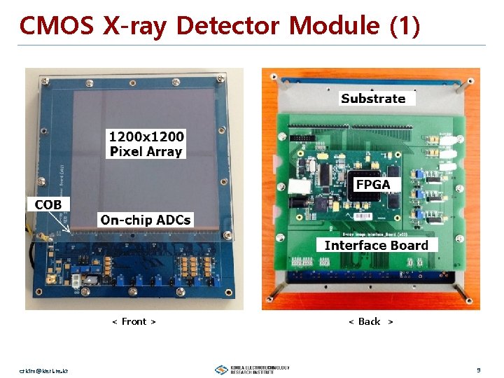
CMOS X-ray Detector Module (1) < Front > crkim@keri. re. kr < Back > 9
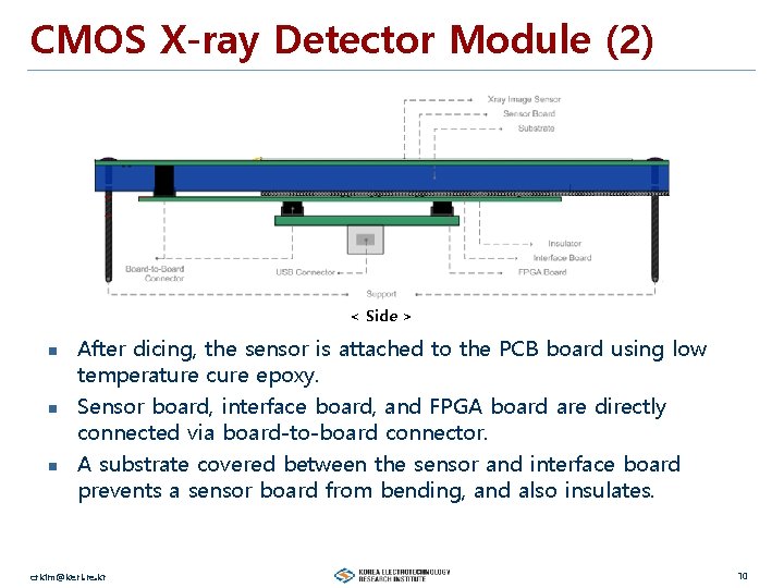
CMOS X-ray Detector Module (2) < Side > n n n After dicing, the sensor is attached to the PCB board using low temperature cure epoxy. Sensor board, interface board, and FPGA board are directly connected via board-to-board connector. A substrate covered between the sensor and interface board prevents a sensor board from bending, and also insulates. crkim@keri. re. kr 10
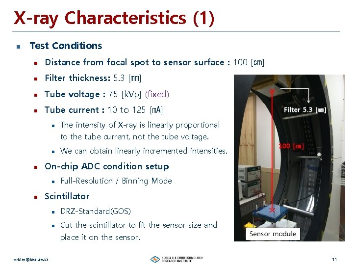
X-ray Characteristics (1) n Test Conditions n Distance from focal spot to sensor surface : 100 [㎝] n Filter thickness: 5. 3 [㎜] n Tube voltage : 75 [k. Vp] (fixed) n Tube current : 10 to 125 [㎃] n The intensity of X-ray is linearly proportional to the tube current, not the tube voltage. n n On-chip ADC condition setup n n We can obtain linearly incremented intensities. Full-Resolution / Binning Mode Scintillator n DRZ-Standard(GOS) n Cut the scintillator to fit the sensor size and place it on the sensor. crkim@keri. re. kr 11
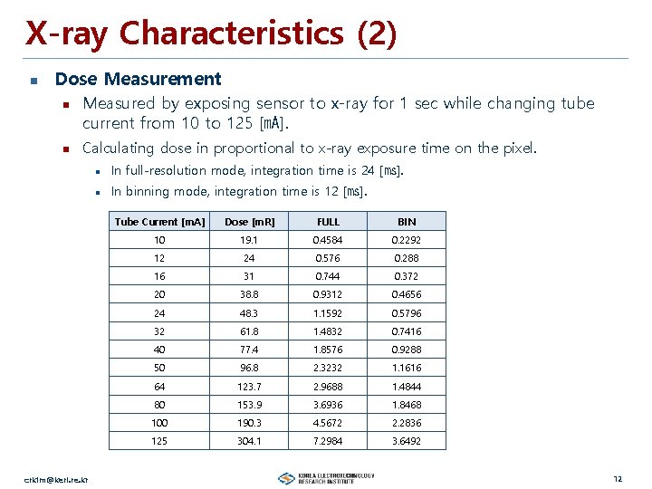
X-ray Characteristics (2) n Dose Measurement n n Measured by exposing sensor to x-ray for 1 sec while changing tube current from 10 to 125 [㎃]. Calculating dose in proportional to x-ray exposure time on the pixel. crkim@keri. re. kr n In full-resolution mode, integration time is 24 [㎳]. n In binning mode, integration time is 12 [㎳]. Tube Current [m. A] Dose [m. R] FULL BIN 10 19. 1 0. 4584 0. 2292 12 24 0. 576 0. 288 16 31 0. 744 0. 372 20 38. 8 0. 9312 0. 4656 24 48. 3 1. 1592 0. 5796 32 61. 8 1. 4832 0. 7416 40 77. 4 1. 8576 0. 9288 50 96. 8 2. 3232 1. 1616 64 123. 7 2. 9688 1. 4844 80 153. 9 3. 6936 1. 8468 100 190. 3 4. 5672 2. 2836 125 304. 1 7. 2984 3. 6492 12
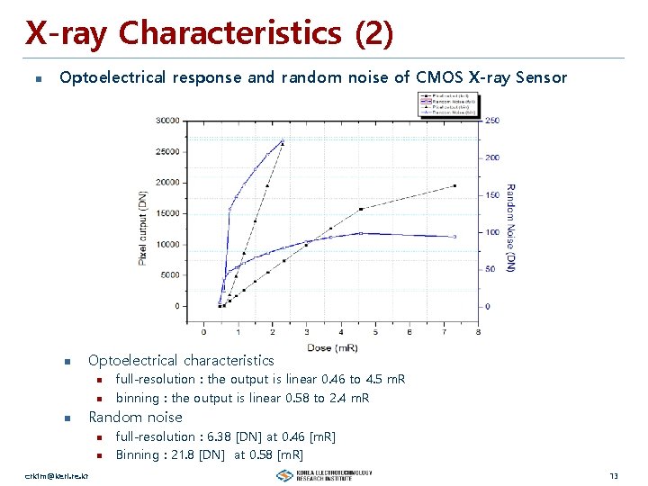
X-ray Characteristics (2) n Optoelectrical response and random noise of CMOS X-ray Sensor n Optoelectrical characteristics n n n full-resolution : the output is linear 0. 46 to 4. 5 m. R binning : the output is linear 0. 58 to 2. 4 m. R Random noise n n crkim@keri. re. kr full-resolution : 6. 38 [DN] at 0. 46 [m. R] Binning : 21. 8 [DN] at 0. 58 [m. R] 13
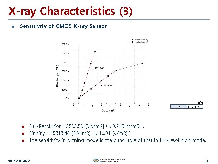
X-ray Characteristics (3) n Sensitivity of CMOS X-ray Sensor 1 LSB n n n [㎶] 63. 258915 Full-Resolution : 3893. 89 [DN/m. R] (≒ 0. 246 [V/m. R] ) Binning : 15818. 48 [DN/m. R] (≒ 1. 001 [V/m. R] ) The sensitivity in binning mode is the quadruple of that in full-resolution mode. crkim@keri. re. kr 14
![X-ray Images (1) n Foot Phantom X-ray exposure condition : 75 [k. Vp] / X-ray Images (1) n Foot Phantom X-ray exposure condition : 75 [k. Vp] /](http://slidetodoc.com/presentation_image_h2/75e5a8aa5ed63d2421c1b0ce0f17074f/image-15.jpg)
X-ray Images (1) n Foot Phantom X-ray exposure condition : 75 [k. Vp] / 64 [m. A] Raw data Contrast Adjusted data Full-Resolution Mode Binning Mode crkim@keri. re. kr 15
![X-ray Images (2) n Hand Phantom X-ray exposure condition : 75 [k. Vp] / X-ray Images (2) n Hand Phantom X-ray exposure condition : 75 [k. Vp] /](http://slidetodoc.com/presentation_image_h2/75e5a8aa5ed63d2421c1b0ce0f17074f/image-16.jpg)
X-ray Images (2) n Hand Phantom X-ray exposure condition : 75 [k. Vp] / 64 [m. A] Raw data Contrast Adjusted data Shaking hand (16 frame) ⇒ Based on consecutive images in full-resolution mode, image lag is negligible. crkim@keri. re. kr 16
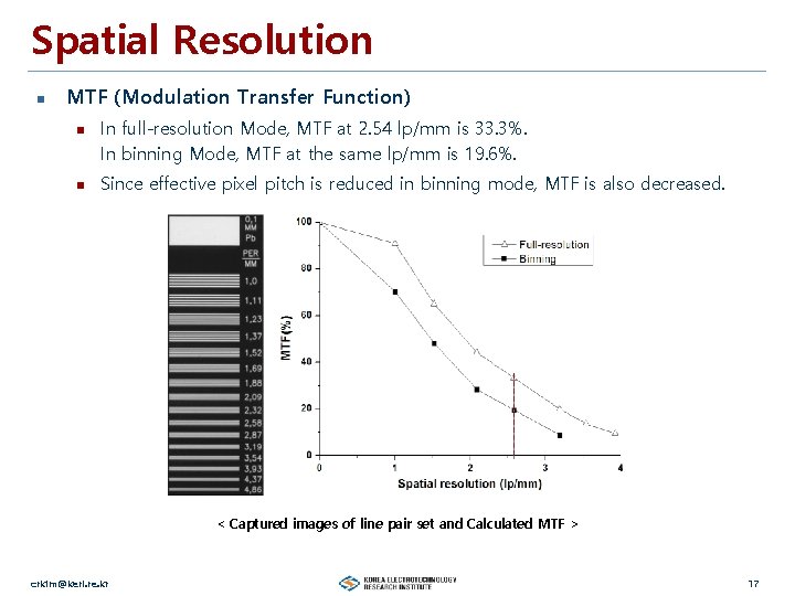
Spatial Resolution n MTF (Modulation Transfer Function) n n In full-resolution Mode, MTF at 2. 54 lp/mm is 33. 3%. In binning Mode, MTF at the same lp/mm is 19. 6%. Since effective pixel pitch is reduced in binning mode, MTF is also decreased. < Captured images of line pair set and Calculated MTF > crkim@keri. re. kr 17
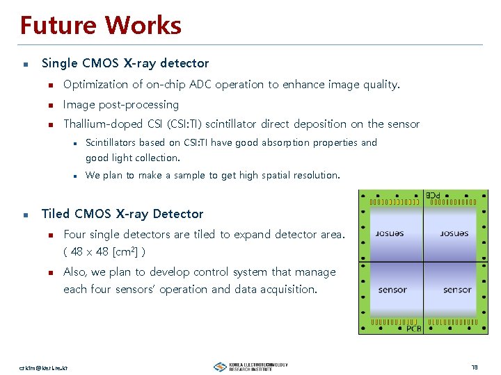
Future Works n Single CMOS X-ray detector n Optimization of on-chip ADC operation to enhance image quality. n Image post-processing n Thallium-doped CSI (CSI: TI) scintillator direct deposition on the sensor n Scintillators based on CSI: TI have good absorption properties and good light collection. n n We plan to make a sample to get high spatial resolution. Tiled CMOS X-ray Detector n Four single detectors are tiled to expand detector area. ( 48 x 48 [cm 2] ) n Also, we plan to develop control system that manage each four sensors’ operation and data acquisition. crkim@keri. re. kr 18
Summary n We developed high-resolution CMOS X-ray detector based on several advantages of CMOS process. n n Also, we measured results such as X-ray linearity as a function of dose, spatial resolution and X-ray images of the objects for performance evaluation with GOS scintillators n n A large-area 1200 x 1200 array CMOS image sensor with full mode(30 fps) and binning mode(60 fps) for mammography and fluoroscopic imaging application. The more detailed characterization of our developed X-ray CMOS image sensor will be evaluated under practical mammography and fluoroscopic application conditions. We plan to enhance the performance of a ingle x-ray detector and to develop tiled x-ray detector process. crkim@keri. re. kr 19

THANK YOU FOR YOUR ATTENTION !
- Slides: 20