High Performance VLSI Design EC 714 Lecture 2


 Ion/Ioff ratio (ii) Time required for a transistor to switch")
 Constant Electric Field scaling �Dennard’s scaling (i) physical dimensions (ii)Voltage and (iii)Doping concentrations")


")

 lead to saturation of velocity at VDS/L of")


 3 to 4 �Ultra low k dielectric 2. 5")

- Slides: 54
High Performance VLSI Design EC 714 Lecture 2 Technology scaling
Content �Introduction of scaling and effects �Device scaling �Small Geometry Effects �Device enhancements �Interconnect scaling �Interconnect enhancement
Introduction of scaling and effects
�Transition phase in High performance IC Design Interconnect Transistor logic Interconne ct
Effect of small size �Effect of interconnects on system data �Power consumption �Noise �Reliability
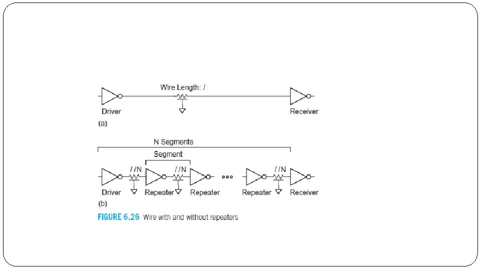
Due to scaling, device delay is reduce but effect on delay due to passive interconnects increases
ITRS Report �“ Interconnect delay is the most critical phenomenon affecting high performance product” 1 um transistor delay = 20 ps 15 nm transistor delay =1. 45 ps But, minimum achievable interconnect delay remains effectively fixed at about 20 ps/mm. Overall speed of modern IC limited by global interconnect
Effect of interconnect delay
�Each additional buffers increases overall power consumption & physical area �Due to global interconnect (i) Delay Increase (ii) power consumption increases (iii) System performance decreases (iv) synchronization faults increases
Variation in supply voltage �Reduce signal integrity �Reduce power integrity
Primary design objectives �Propagation delay �Power consumption �Noise
Device scaling �Higher packing density>>yield �Higher circuit speed>>enhance transistor performance �Higher system speed>>smaller chip to chip delay �Lower system power consumption>> smaller chip to chip capacitive loads �Enhanced system reliability>>fewer leads and off chip connection �Heterogeneous system integration
Types of scaling Constant voltage scaling: 2 um to 0. 8 um Constant electric field scaling: 0. 8 um to 130/90 nm Structural enhancement: below 45 nm Constant voltage scaling: below 130/90 nm
Types of scaling: Effect
MOS Operation
Digital IC Performance (i) Ion/Ioff ratio (ii) Time required for a transistor to switch from the on state to off state
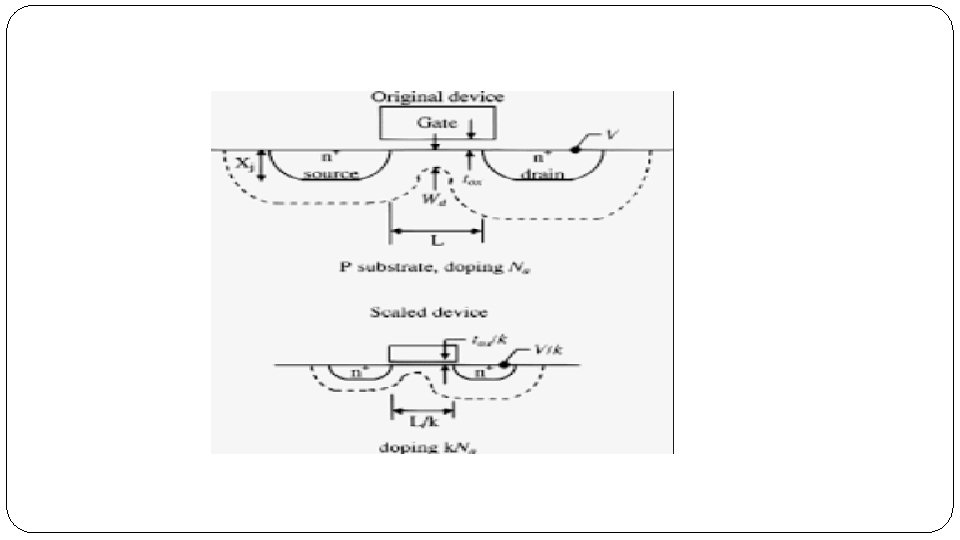
(i) Constant Electric Field scaling �Dennard’s scaling (i) physical dimensions (ii)Voltage and (iii)Doping concentrations
1. Increse the current drive capacity by scaling the tox and L 2. Control the high vertical electric field and power dissipation by scaling vdd 3. Maintain current drive capability by scaling vt 4. Decrease the depletion layer width by increasing the substrate doping concentration.
Subthreshold slope
Constant Field Scaling �Increase the current drive capability by scaling gate insulator thickness and channel length �Control the high vertical electric field and power dissipation by scaling power supply voltage �Maintain current drive capability by scaling the threshold voltage �Decease the depletion width by increasing the substrate doping concentration
Device enhancement �Small geomentry effects degrade the device performance and increase leakage currents �Below 90 nm these effect negate speed gains
VTH roll off �Vth of device depends on �Work function difference (flat band voltage) and surface potential do not change with device geometry �The voltage across insulator due to depletion region charge due to gate voltage also due to source drain depletion region extend below the channel �Due to this the Vth is higher than it should be for the short channel �i. e. Vth increase due to source drain depletion region induced charge
DIBL �Due to decrease in source drain barrier with scaling length of channel �At VGS=0 and VDS=VDD large current flow from source to darin to substrate �Reduce Threshold voltage depend on VDS
Velocity saturation �Higher VDS/L (lateral field) lead to saturation of velocity at VDS/L of 100000 v/cm velocity saturates 107 cm/s for electron 106 cm/s for hole �Velocity should be proportional to E but beyond 1 MV/cm it saturates so it degade the moility due to. Gunupudi increase in lattice interaction and Pavan collision of charge carriers �Overall effect is drain current is now less quadratic than erlier so it is lower �So Shockley model is fail to estimate drain current �So sakurai alpha power model is valid where alpha is etween 1 and 2 typically 1. 3
Mobility degradation �Mobility of charge carrier degrade due to increase in vertical field VGS/tox �Increase of lattice collision and scattering effect lead to degradation of mobility of electron and hole �Electron mobility 200 cm 2/v. s and hole is 50 cm 2/v. s at 2 MV/cm filed �Overall current is reduced
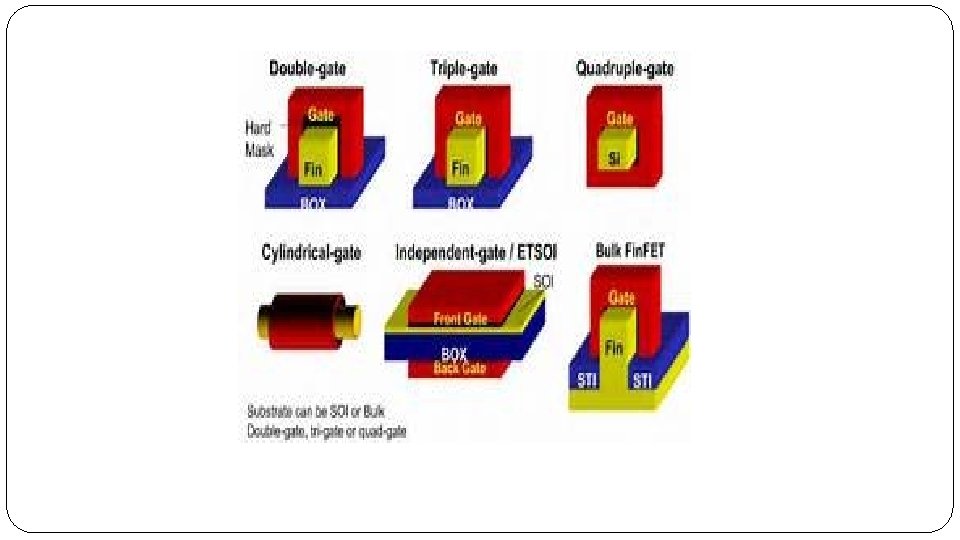
Device enhancement �To supress small geometry effect �Enhance device mobility and velocity �Non uniform channel doping �Strain engineering �High k and metal gate combined �Multi gate devices
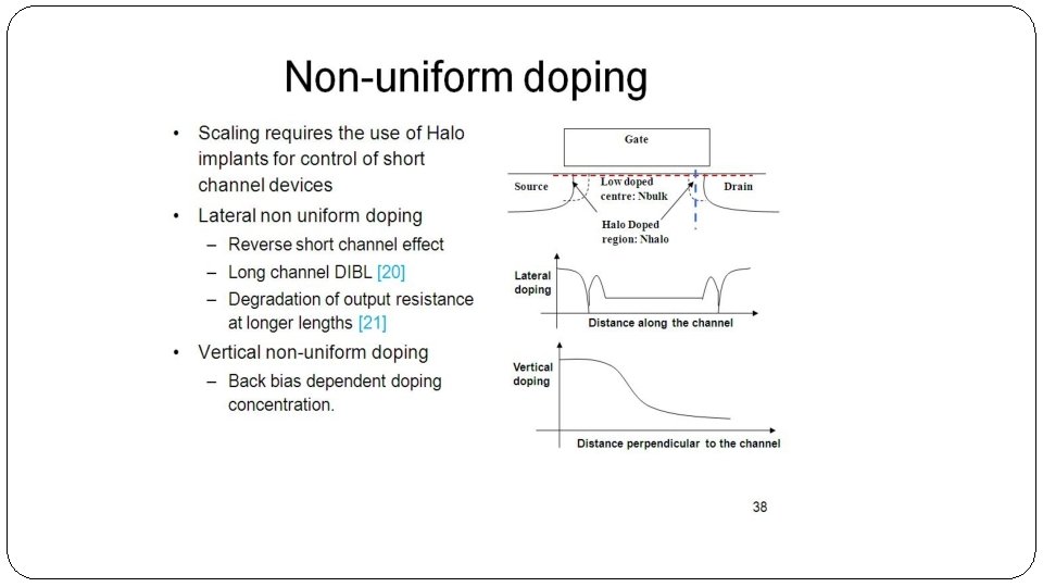
Non uniform channel doping �Higher doping concentration in S/D near channel �Reduce S/D depletion �Reduce Vt roll off �Increase carrier mobility
Strain engineering �Beyond 90 nm molecule is strained to �Improve mobility of carriers there by changing scattering characteristics �Substrate induce strain �Process induced strain
High K and metal gate combined �Below 65 nm �Gate dielectric is changed to hafnium oxide �To reduce leakage �Short channel effect �EOT of 0. 9 nm behaves as EOT of 32 nm
Improve the performance beyond 90 nm �Increase the mobility �Improving the device structure �Non uniform Channel doping �Strain Engineering �High K and Metal gate structures to reduce the leakage
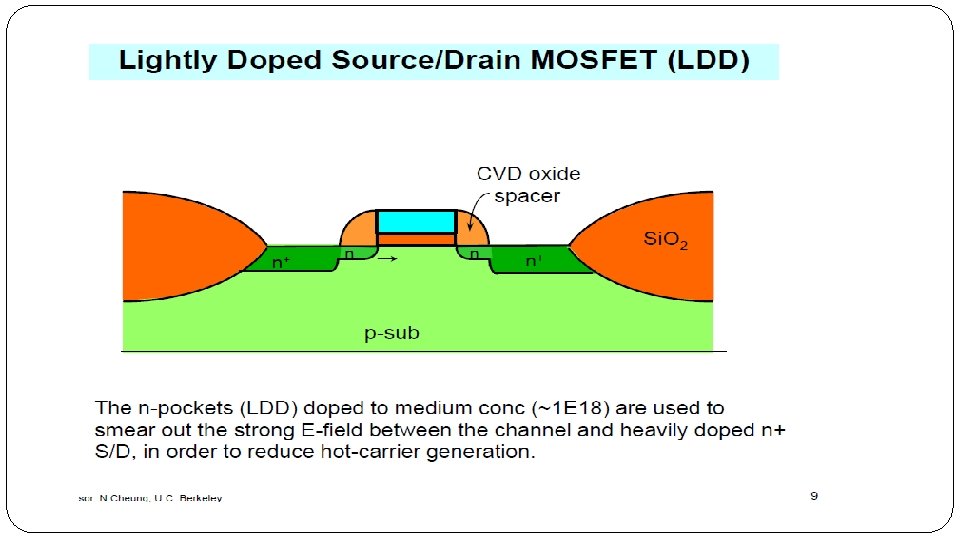
Non uniform channel doping Due to high substare doping Thresold voltage increase and carrier mobility decease also vth roll off and DIBL effects To overcome the above effects, LDD structures are used It reduce the depletion region widths below source drain and as a result it reduces DIBL , HOT carrier and Vth roll off effects
Strain Engineering �Increse the carrier mobility beyond 90 nm �If a molecule is strained the energy band structure of molecule changes due to stress ; mobility changes �Substrate induced starin �Process induced strain
Interconnect
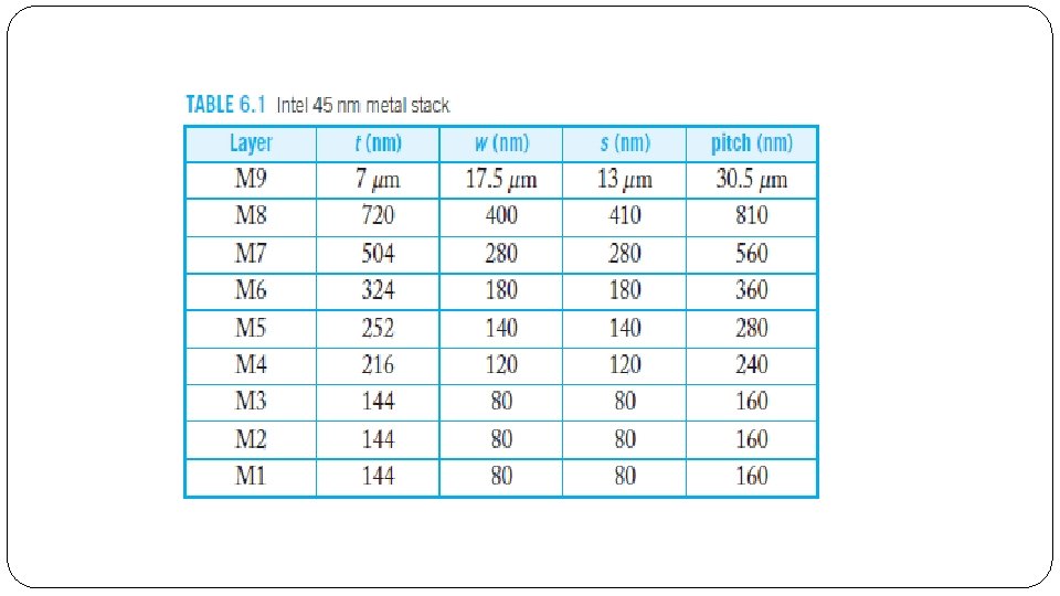
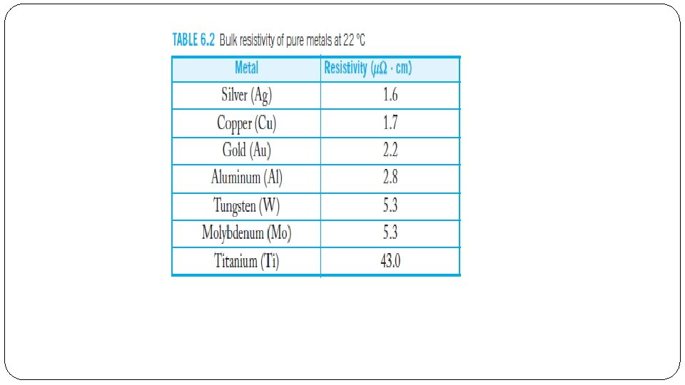
Resistance of Interconnect �Resistance
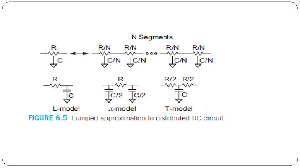
Capacitance 42 Deep Submicron VLSI Des. Lec. 6 January 31, 2022
Wire Capacitance � Wire has capacitance per unit length �To neighbors �To layers above and below � Ctotal = Ctop + Cbot + 2 Cadj 43 Deep Submicron VLSI Des. Lec. 6 January 31, 2022
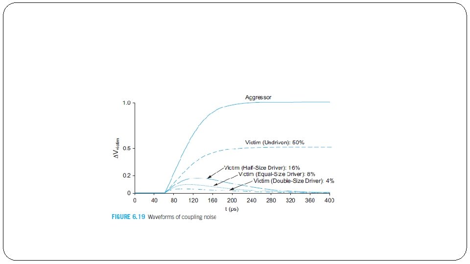
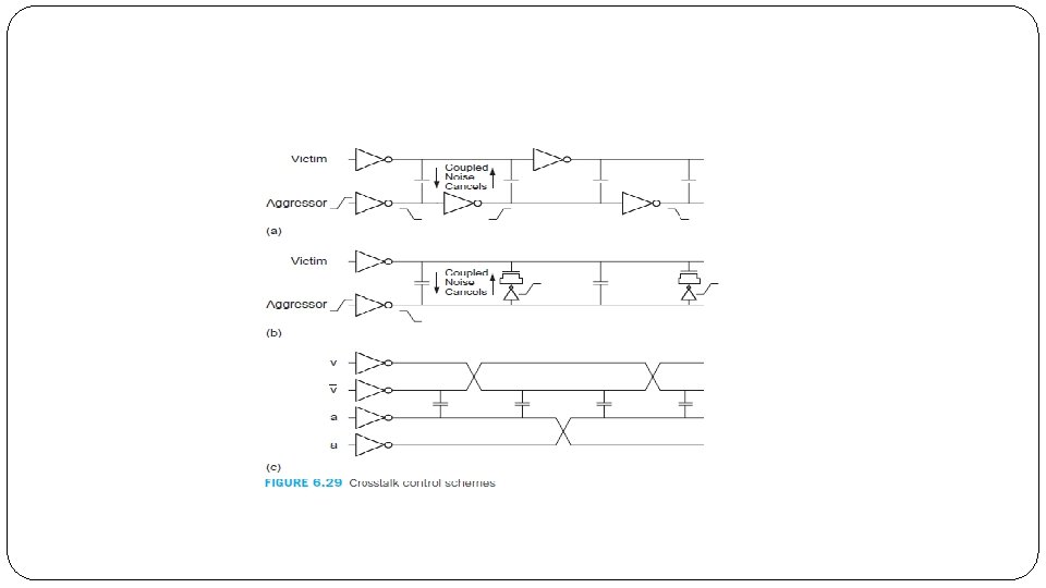
Crosstalk
Control cross talk �Increase spacing to adjucent lines �Shield wires �Ensure neighbour switch at different time �Cross talk cancellation
Interconnect Impact �delay
Interconnect Scaling �Ideal scaling: Global wirelength increase by factor S due to increase in overall die area by factor Sc ; local wire length reduced by factor s due to gate pitch reduction by factor s 2 �Quasi ideal scaling: vertical dimensions scaled by factor 1/√ s compared to horizontal �Scaling based on constant resistance Local and global wire resistance remain constant �Scaling based on constant thickness Local and global wire thickness remain constant
Interconnect enhancement �Ultra low K dielectric material has following advantages �Interconnect parasitic capacitance reduce �Reduction in dynamic power consumption since overall switching capacitance decease �Indirect reduction in interconnect parasitic resistance since a lower dielectric constant enables a greater interconnect thickness at a constant lateral capacitance
Other Low K dielectrics for Interconnect �Carbon doped Silicon �Porous dielectric film �Spin on Dielectric �Air gap based dielectric
�Organic silicon(Sico. H) 3 to 4 �Ultra low k dielectric 2. 5
Other options �On chip optical interconnect �Carbon based on chip interconnect �Graphene Nano ribbons