High Performance Scalable Base4 Fast Fourier Transform Mapping

High Performance Scalable Base-4 Fast Fourier Transform Mapping Greg Nash Centar 2003 High Performance Embedded Computing Workshop www. centar. net

Outline • Base-4 transformation for calculating DFT • Mapping methodology • Direct form DFT architecture • FFT architecture • Performance
 • Multiplications =")
Discreet Fourier Transform • Mathematical form: • Matrix form Z=CX: (N=16) • Multiplications = N 2

Base-4 Matrix Equation • Find reordering permutation P • DFT matrix equation becomes where
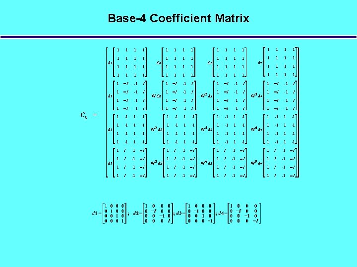
 • Form for N=16 “ ”= element by")
Base-4 DFT Matrix Equation (Compact Form) • Form for N=16 “ ”= element by element multiply • General Form

Base-4 DFT Equation Characteristics • Coefficient matrices represent series of 4 -point transforms: where Takes advantage of reduced arithmetic with radix r = 4 butterfly, but transform length not limited to N = r m Transform length must be divisible by 16 • CM 1 and CM 2 contain only elements from the set CM 1 X and CM 2 Yt only involve complex additions • Twiddle factor matrix WM is of size N/4 x N/4 rather than N x N x 16 fewer multiplies than original DFT equation (Z=CX)

Systolic Array Example: Matrix Multiply • Algorithm: • Space-time mapping: computations at {i, j, k} “mapped” to indices {time, x, y} e Project along time axis c “Space-Time” View d Systolic Array: Each intersection point corresponds to a “processing element” (PE) that receives data from its neighbors, does a multiply-add, and passes the result to adjacent PEs, once per time cycle.

Find Systolic Architecture Using SPADE Mathematical Algorithm for j to N/4 do for k to N/4 do Y[j, k]: =WM[j, k]*add(CM 1[j, i]*X[i, k], i=1. . 4); od; for k to 4 do Z[k, j] : = add(CM 2[k, i]*Y[j, i], i=1. . N/4); od od; † Simulator, Graphical Outputs Input Code Architectural Constraints Objective Functions Variable position, area, regularity, bandwidth Automatic Search for Space-Time Transformations, T †Symbolic Parallel Algorithm Development Environment

SPADE Functionality • SPADE accepts input statements of the affine form – Where Ax, By/ax, by are integer matrices/vectors, S is the dimension of the algorithm space and the “depends on” includes commutative and associative operators: min, max, , • SPADE finds latency optimal systolic designs subject to constraints imposed by scheduling, localization, reindexing, and allocation • Secondary objective functions used to select architectures are minimum area, maximum regularity and minimum network bandwidth

Systolic Array Designs: Minimum Area X IM 2 X N/4=16 CM 1 CM 2 IM 1 CM 1 Z Y Space-Time Views (N=64) Z 4 Example Systolic Array Views (N=64) Multipliers Adders CM 2 Y X • • • Latency (cycles) = N/2 + 8 Six unique designs Throughput (cycles/block) = N/4 + 6 WM mapped to same space-time location as Y IM 1 and IM 2 variables (SPADE created) perform matrix multiply/adds
 Z 4 Z")
Systolic Array Designs: Maximum Regularity • • • Systolic Arrays (N=32) Z 4 Z Two unique designs found Throughput and latency optimal Latency (cycles) = N/2 + 8 Throughput (cycles/block) = N/4 +1 WM mapped to same space-time position as Y Y N/4 = 8 X CM 2 Z CM 1 Y Adders IM 1 Multipliers Adders CM 2 Transformations CM 2 X Z CM 1 Y Space-time view (N=32) X CM 2
 CM 1 X Y Z CM")
Systolic Architecture to Array Design Systolic Architecture (N=32) CM 1 X Y Z CM 2 Array Design (N=32)

Altera Stratix FPGA: DFT Mapping Systolic DFT Array

1 D FFT via Factorization • Factor N = N 1 * N 2 • Creat a 2 -D matrix with N 1 rows by N 2 columns, (assume N 1 > N 2), • Do N 2 1 -D “column” DFTs followed by N 1 “row” DFTs: • If N 1 N 2 then (linear) array size can be reduced from O( N 1 N 2 ) to O(N 1) with minimal effect on throughput: – Cycles for N/4 array (no factorization) = N/4 + 1 – Cycles for N 1 /4 array = N 1 (N 1 /4 + 1) + twiddle mult N/2 • Can do 2 -D DFT by not performing twiddle multiplication WN • Use base-4 DFT mapping to do all row/column DFTs

Base-4 Factorization Architecture DFT Output Z 2 “row” DFTs Z Y CM 1 X Z • N = 1024 points • N = N 1 * N 2 • N 1 = N 2 = 32 • Uses both of the two optimal systolic designs • Twiddle multiplications not shown • Throughput/latency optimal except for interstage delay Z 2 “column” DFTs CM 2 X CM 1 Two Space-Time Views (only two of N 1 iterations shown) DFT Input

Two DFT Architectures Combined • Shown for N = 1024 points • N = N 1 * N 2 • N 1 = N 2 = 32 • M = 512 bits (16 bit word)
 • Z")
1 st to 2 nd Stage Data Formatting Problem (32 Point DFT) • Z CM 1 DFT data positions of 1 st stage output sequences . . . Y CM 2 X • Z Desired data positions for input sequences to 2 nd stage Y CM 2 X CM 1 . . .

Interstage Data Formatting via “On-the-Fly” Permutations • New code with matrix rotation steps • New DFT first stage output sequences . . .

1 -D DFT Performance Estimates Based on: • Register transfer level behavioral simulation of 1024 point DFT • Partially populated layout • Timing analysis using Altera Stratix EP 1 S 60 FPGA chip • 16 bit fixed-point word length

Latency • Base-4 FFT pipeline depth is nominally N 1 /4+ 9 << N N 1 /4 longest path (red) • 9 Latency (cycles) 1/Throughput (cycles-1) when complete X available

Partitioning to Scale Computations to Application • Use an array “section” to perform partially processed result • Partial results accumulated at output • Memory needed scales with partition size Fully Parallel Array Partitioned Array
 • • Example: 512 -point FFT")
Non-Square 2 -D Inputs (N 1 N 2) • • Example: 512 -point FFT (N 1 = 32, N 2 = 16) On-the-fly permutations for correct data placement Columns: Compute 16 32 -point DFTs Rows: Compute 2 sets of 16 16 -point DFTs

Example Resource Usage†: 1024 Point DFT † Altera Stratix EP 1 S 60 F 1508 C 6 FPGA chip (16 bit fixed point)

Base-4 DFT Architecture Summary • • • High performance 1 -D and 2 -D DFTs Based on latency and throughput optimal parallel circuits Transform size not restricted to N = rm Latency 1/throughput when entire input block available Architecture is scaleable and easily parameterized Design is simple, regular, local and synchronous Fast convolutions naturally supported Natural partitioning strategies exist Pseudo-linear architecture good fit to latest generation of FPGA chips

More Information at www. centar. net • “Automatic Generation of Systolic Array Designs For Reconfigurable Computing” , Proc. Engineering of Reconfigurable Systems and Algorithms (ERSA '02), International Multiconference in Computer Science, Las Vegas, Nevada, June 24, 2002. – General description of SPADE – Faddeev algorithm (Find CX+D, given AX=B, X is unknown) • Constraint Directed CAD Tool For Automatic Latency-Optimal Implementations, SPIE ITCom 2002, Boston, Massachussetts, July 29 -August 2, 2002. – Use of constraints as a filter of systolic designs – 2 -D Discreet Fourier transforms using base-4 architecture
- Slides: 26