High Performance Asynchronous ASIC BackEnd Design Flow Using

High Performance Asynchronous ASIC Back-End Design Flow Using Single-Track Full-Buffer Standard Cells Marcos Ferretti, Recep O. Ozdag, Peter A. Beerel Department of Electrical Engineering Systems University of Southern California USC Asynchronous CAD/VLSI Group
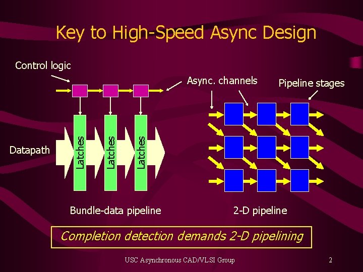
Key to High-Speed Async Design Control logic Pipeline stages Latches Datapath Latches Async. channels Bundle-data pipeline 2 -D pipeline Completion detection demands 2 -D pipelining USC Asynchronous CAD/VLSI Group 2
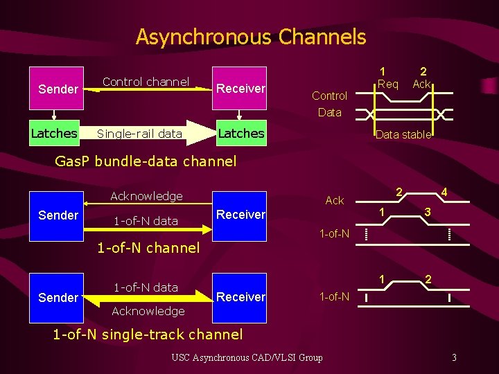
Asynchronous Channels Sender Latches Control channel Single-rail data Receiver Control Data Latches 1 Req 2 Ack Data stable Gas. P bundle-data channel Acknowledge Sender 1 -of-N data Ack Receiver Sender 4 1 3 1 2 1 -of-N channel 1 -of-N data 2 Receiver 1 -of-N Acknowledge 1 -of-N single-track channel USC Asynchronous CAD/VLSI Group 3
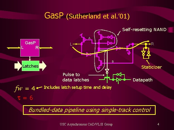
Gas. P (Sutherland et al. ’ 01) Self-resetting NAND A Gas. P L R R L B Latches Staticizer Pulse to data latches fw = 4 t=6 Datapath Includes latch setup time and delay Bundled-data pipeline usingle-track control USC Asynchronous CAD/VLSI Group 4
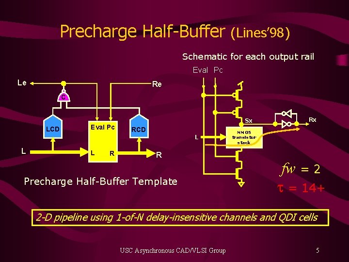
Precharge Half-Buffer (Lines’ 98) Schematic for each output rail Eval Pc Le Re C LCD Eval Pc Sx RCD L L L R R Precharge Half-Buffer Template Rx NMOS transistor stack fw = 2 t = 14+ 2 -D pipeline using 1 -of-N delay-insensitive channels and QDI cells USC Asynchronous CAD/VLSI Group 5
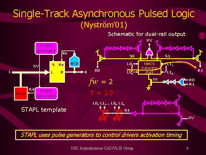
Single-Track Asynchronous Pulsed Logic (Nyström’ 01) Schematic for dual-rail output Pulse generator xv L S L R 4 Reset xv Re Re R Pulse generator S 0 RCD L 01 R R 0 L 0 n fw = 2 t = 10 S 1 NMOS transistor stack L 11 R 1 L 1 n re R 0 R 1 L 01 L 11… L 0 n L 1 n STAPL template R 4 xv STAPL uses pulse generators to control drivers activation timing USC Asynchronous CAD/VLSI Group 6
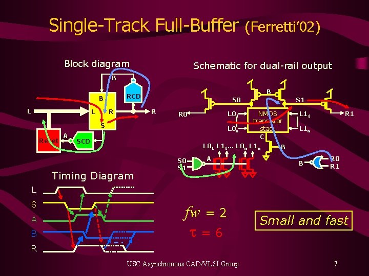
Single-Track Full-Buffer Block diagram (Ferretti’ 02) Schematic for dual-rail output B B L L B RCD R S 0 R R 0 S Reset A SCD Timing Diagram S 0 S 1 L 01 S 1 NMOS transistor L 0 n stack C L 01 L 11… L 0 n L 1 n B A L 11 R 1 L 1 n B R 0 R 1 L S A B fw = 2 t=6 Small and fast R USC Asynchronous CAD/VLSI Group 7
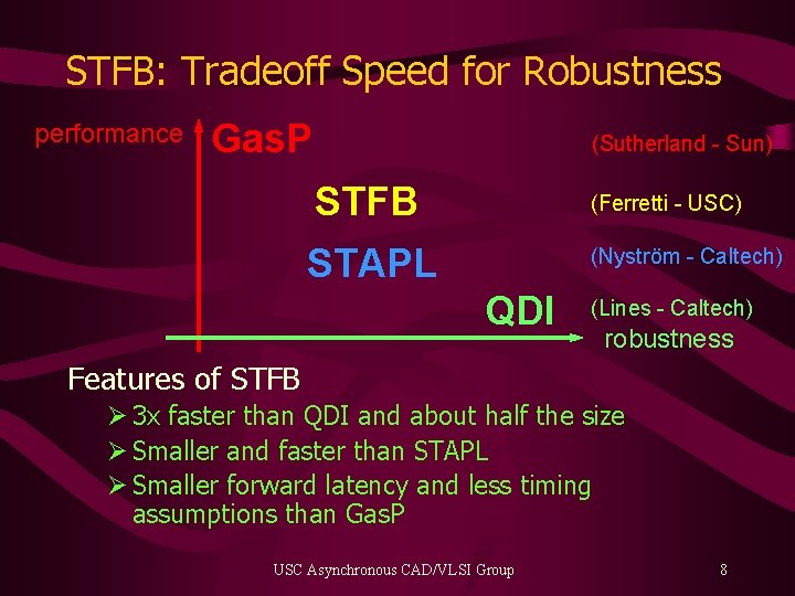
STFB: Tradeoff Speed for Robustness performance Gas. P (Sutherland - Sun) STFB (Ferretti - USC) STAPL (Nyström - Caltech) QDI (Lines - Caltech) robustness Features of STFB Ø 3 x faster than QDI and about half the size Ø Smaller and faster than STAPL Ø Smaller forward latency and less timing assumptions than Gas. P USC Asynchronous CAD/VLSI Group 8
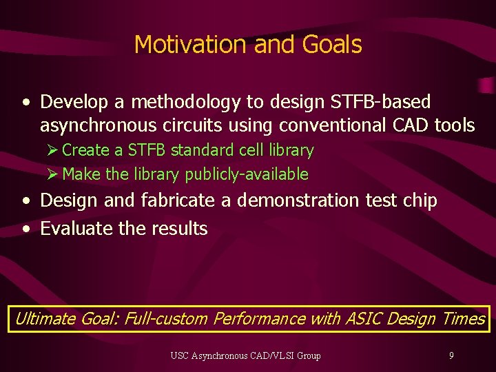
Motivation and Goals • Develop a methodology to design STFB-based asynchronous circuits using conventional CAD tools Ø Create a STFB standard cell library Ø Make the library publicly-available • Design and fabricate a demonstration test chip • Evaluate the results Ultimate Goal: Full-custom Performance with ASIC Design Times USC Asynchronous CAD/VLSI Group 9
Outline STFB standard-cell design Backend design flow Demonstration test chip Conclusions USC Asynchronous CAD/VLSI Group 10
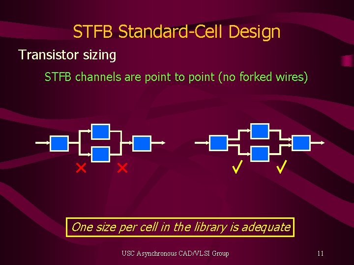
STFB Standard-Cell Design Transistor sizing STFB channels are point to point (no forked wires) One size per cell in the library is adequate USC Asynchronous CAD/VLSI Group 11
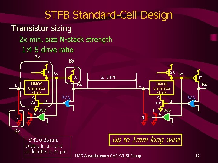
STFB Standard-Cell Design Transistor sizing 2 x min. size N-stack strength 1: 4 -5 drive ratio 2 x 8 x 2. 8 Sx L 5 NMOS transistor stack C B Wn A 10 Rx 2. 8 Sx ≤ 1 mm NMOS transistor stack C B Wn L RCD SCD 8 x TSMC 0. 25 mm, widths in mm and all lengths 0. 24 mm 5 A 10 Rx RCD SCD Up to 1 mm long wire USC Asynchronous CAD/VLSI Group 12
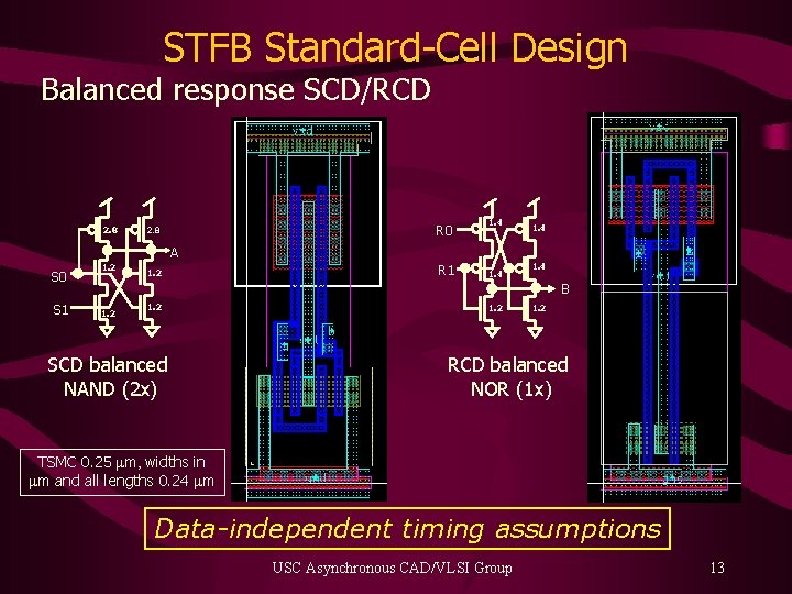
STFB Standard-Cell Design Balanced response SCD/RCD 2. 8 R 0 2. 8 1. 4 A S 0 S 1 1. 2 R 1 1. 4 B 1. 2 SCD balanced NAND (2 x) 1. 2 RCD balanced NOR (1 x) TSMC 0. 25 mm, widths in mm and all lengths 0. 24 mm Data-independent timing assumptions USC Asynchronous CAD/VLSI Group 13
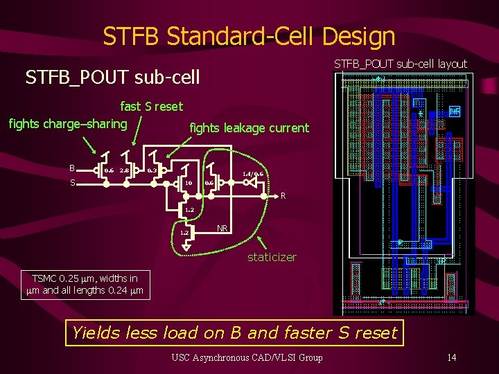
STFB Standard-Cell Design STFB_POUT sub-cell layout STFB_POUT sub-cell fast S reset fights charge–sharing fights leakage current B 0. 6 2. 8 S 0. 3 1. 4/0. 6 10 0. 6 R 1. 2 NR staticizer TSMC 0. 25 mm, widths in mm and all lengths 0. 24 mm Yields less load on B and faster S reset USC Asynchronous CAD/VLSI Group 14
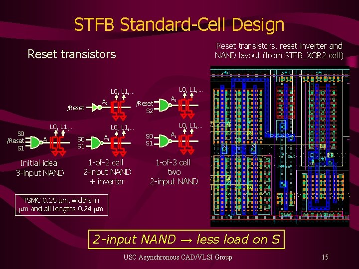
STFB Standard-Cell Design Reset transistors, reset inverter and NAND layout (from STFB_XOR 2 cell) Reset transistors L 01 L 11… /Reset S 0 /Reset S 1 A 2 L 01 L 11… A Initial idea 3 -input NAND /Reset S 2 L 01 L 11… S 0 S 1 A 1 S 0 S 1 1 -of-2 cell 2 -input NAND + inverter A 2 A 1 1 -of-3 cell two 2 -input NAND TSMC 0. 25 mm, widths in mm and all lengths 0. 24 mm 2 -input NAND → less load on S USC Asynchronous CAD/VLSI Group 15
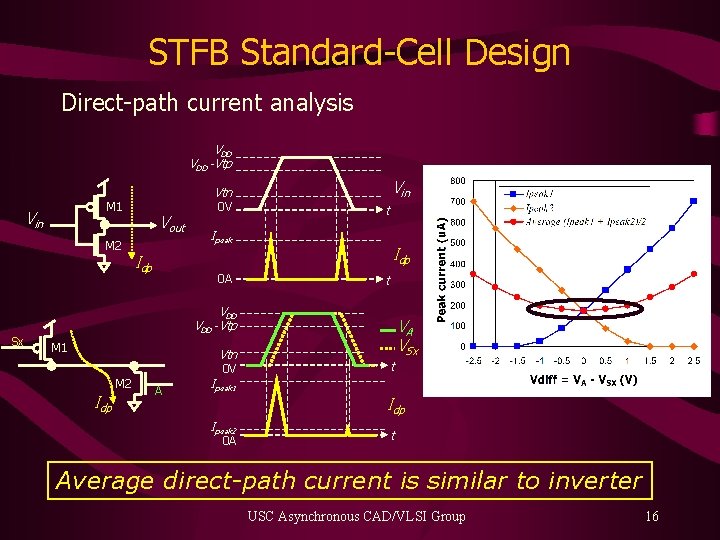
STFB Standard-Cell Design Direct-path current analysis VDD -Vtp M 1 Vin M 2 Sx Vin Vtn Vout Idp 0 V t Ipeak 0 A Idp t VDD -Vtp M 1 Vtn 0 V M 2 Idp A VA VSx t Ipeak 1 Idp Ipeak 2 0 A t Average direct-path current is similar to inverter USC Asynchronous CAD/VLSI Group 16
Outline STFB standard cell design Backend design flow Demonstration test chip Conclusions USC Asynchronous CAD/VLSI Group 17
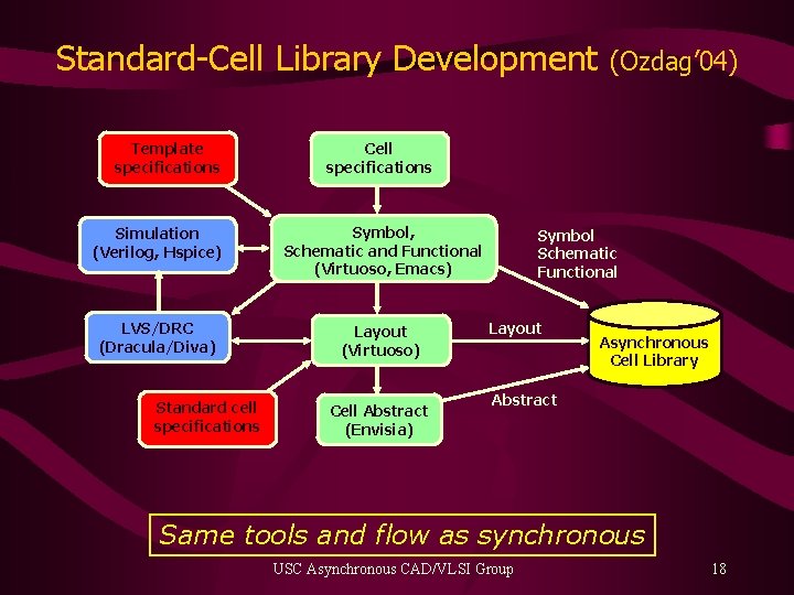
Standard-Cell Library Development Template specifications Cell specifications Simulation (Verilog, Hspice) Symbol, Schematic and Functional (Virtuoso, Emacs) LVS/DRC (Dracula/Diva) Layout (Virtuoso) Standard cell specifications (Ozdag’ 04) Cell Abstract (Envisia) Symbol Schematic Functional Layout Asynchronous Cell Library Abstract Same tools and flow as synchronous USC Asynchronous CAD/VLSI Group 18
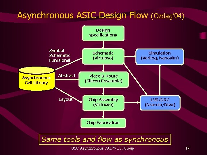
Asynchronous ASIC Design Flow (Ozdag’ 04) Design specifications Symbol Schematic Functional Asynchronous Cell Library Schematic (Virtuoso) Abstract Place & Route (Silicon Ensemble) Layout Chip Assembly (Virtuoso) Simulation (Verilog, Nanosim) LVS/DRC (Dracula/Diva) Chip Fabrication Same tools and flow as synchronous USC Asynchronous CAD/VLSI Group 19
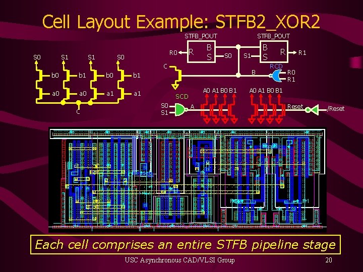
Cell Layout Example: STFB 2_XOR 2 STFB_POUT S 0 S 1 R 0 S 0 R B S STFB_POUT S 0 C b 0 b 1 a 0 a 1 C S 1 B A 0 A 1 B 0 B 1 SCD S 0 S 1 B S A R RCD R 1 R 0 R 1 A 0 A 1 B 0 B 1 Reset /Reset Each cell comprises an entire STFB pipeline stage USC Asynchronous CAD/VLSI Group 20

Outline STFB standard cell design Backend design flow Demonstration test chip Conclusions USC Asynchronous CAD/VLSI Group 21
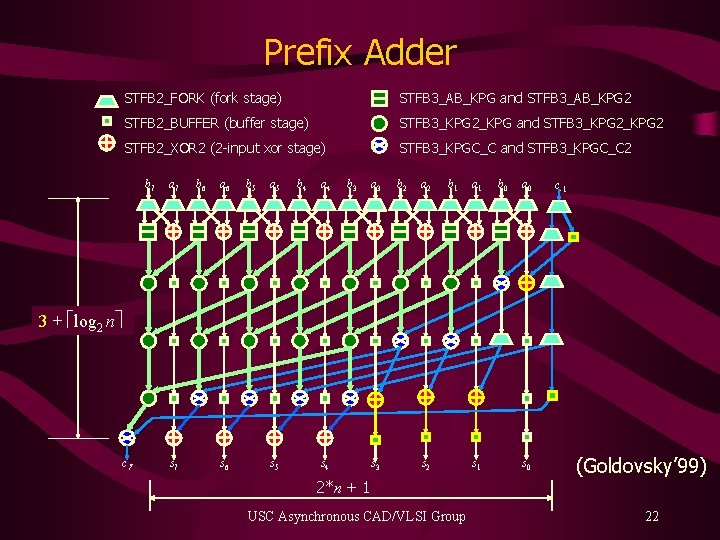
Prefix Adder STFB 2_FORK (fork stage) STFB 3_AB_KPG and STFB 3_AB_KPG 2 STFB 2_BUFFER (buffer stage) STFB 3_KPG 2_KPG and STFB 3_KPG 2 STFB 2_XOR 2 (2 -input xor stage) STFB 3_KPGC_C and STFB 3_KPGC_C 2 b 7 a 7 b 6 a 6 b 5 a 5 b 4 a 4 b 3 a 3 b 2 a 2 b 1 a 1 b 0 a 0 c-1 3 + élog 2 nù c 7 s 6 s 5 s 4 s 3 s 2 2*n + 1 USC Asynchronous CAD/VLSI Group s 1 s 0 (Goldovsky’ 99) 22
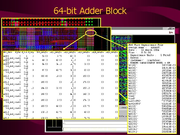
64 -bit Adder Block Silicon Ensemble P&R Schematic (Virtuoso) Place & Route (Silicon Ensemble) Floor plan Input pins on the left (A 64, B 64 and C) M 4 M 5 129 and rows Output pins power grid on thearea right 70% (S utilization 64 and C) Plan power Pins and cell placement Filler cell Routing USC Asynchronous CAD/VLSI Group 23
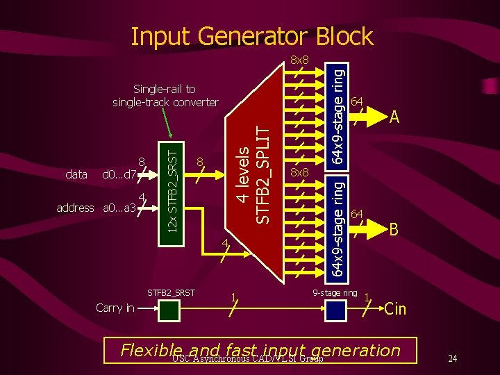
Input Generator Block 64 x 9 -stage ring 8 x 8 address a 0…a 3 4 8 4 STFB 2_SRST Carry in 1 64 A 8 x 8 64 x 9 -stage ring d 0…d 7 4 levels STFB 2_SPLIT data 8 12 x STFB 2_SRST Single-rail to single-track converter 64 9 -stage ring B 1 Cin Flexible and fast input generation USC Asynchronous CAD/VLSI Group 24
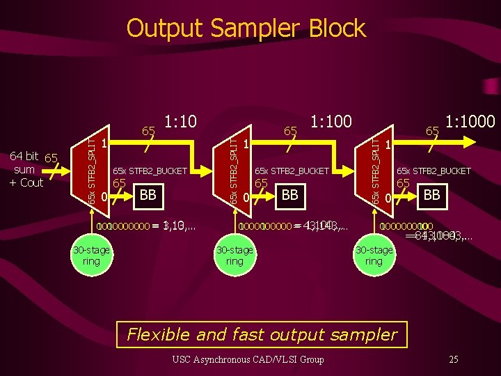
1 1: 10 65 x STFB 2_BUCKET 0 65 BB 1, 10, … 100000 = 3, 13, … 0010000000 30 -stage ring 65 1 1: 100 65 x STFB 2_BUCKET 0 65 BB = 43, 143, … 1, 100, … 100000= 0000100000 30 -stage ring 65 x STFB 2_SPLIT 65 65 x STFB 2_SPLIT 64 bit 65 sum + Cout 65 x STFB 2_SPLIT Output Sampler Block 65 1 1: 1000 65 x STFB 2_BUCKET 65 0 BB 10000000100 1, 1000, … ==843, 1843, … 30 -stage ring Flexible and fast output sampler USC Asynchronous CAD/VLSI Group 25
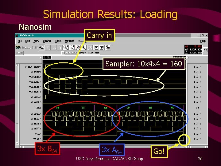
Simulation Results: Loading Nanosim Carry in Sampler: 10 x 4 x 4 = 160 3 x B 64 3 x A 64 USC Asynchronous CAD/VLSI Group Go! 26
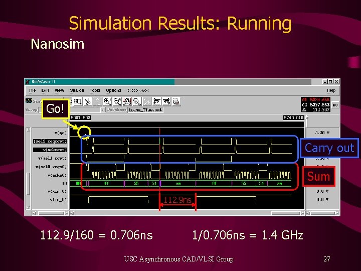
Simulation Results: Running Nanosim Go! Carry out Sum 112. 9 ns 112. 9/160 = 0. 706 ns 1/0. 706 ns = 1. 4 GHz USC Asynchronous CAD/VLSI Group 27
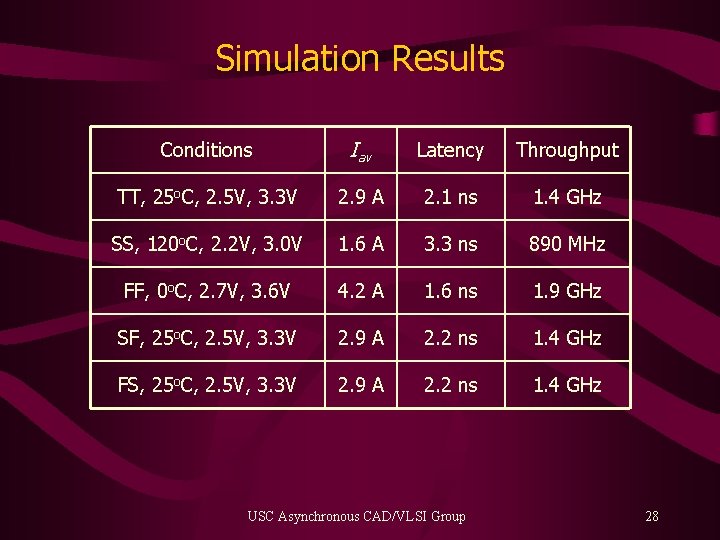
Simulation Results Conditions Iav Latency Throughput TT, 25 o. C, 2. 5 V, 3. 3 V 2. 9 A 2. 1 ns 1. 4 GHz SS, 120 o. C, 2. 2 V, 3. 0 V 1. 6 A 3. 3 ns 890 MHz FF, 0 o. C, 2. 7 V, 3. 6 V 4. 2 A 1. 6 ns 1. 9 GHz SF, 25 o. C, 2. 5 V, 3. 3 V 2. 9 A 2. 2 ns 1. 4 GHz FS, 25 o. C, 2. 5 V, 3. 3 V 2. 9 A 2. 2 ns 1. 4 GHz USC Asynchronous CAD/VLSI Group 28
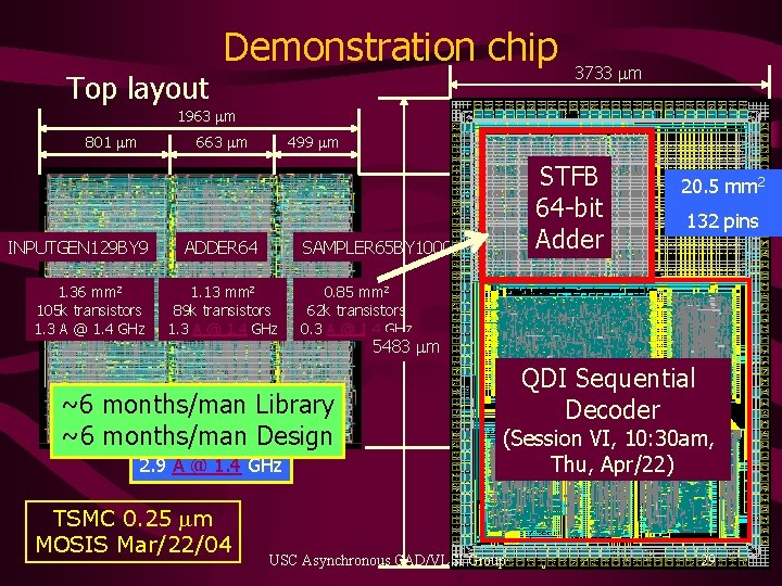
Top layout Demonstration chip 3733 mm 1963 mm 801 mm 663 mm INPUTGEN 129 BY 9 1. 36 mm 2 105 k transistors 1. 3 A @ 1. 4 GHz 499 mm ADDER 64 SAMPLER 65 BY 1000 1. 13 mm 2 89 k transistors 1. 3 A @ 1. 4 GHz 0. 85 mm 2 62 k transistors 0. 3 A @ 1. 4 GHz ~6 months/man Library 3. 3 mm 2 ~6 months/man Design 257 k transistors 2. 9 A @ 1. 4 GHz TSMC 0. 25 mm MOSIS Mar/22/04 STFB 64 -bit Adder 20. 5 mm 2 132 pins 1700 mm 5483 mm QDI Sequential Decoder (Session VI, 10: 30 am, Thu, Apr/22) USC Asynchronous CAD/VLSI Group 29
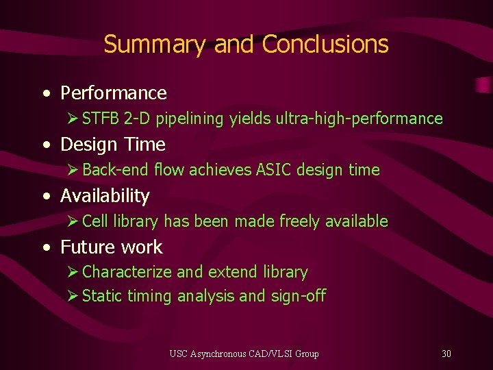
Summary and Conclusions • Performance Ø STFB 2 -D pipelining yields ultra-high-performance • Design Time Ø Back-end flow achieves ASIC design time • Availability Ø Cell library has been made freely available • Future work Ø Characterize and extend library Ø Static timing analysis and sign-off USC Asynchronous CAD/VLSI Group 30
Efharisto! (Thank you!) USC Asynchronous CAD/VLSI Group 31
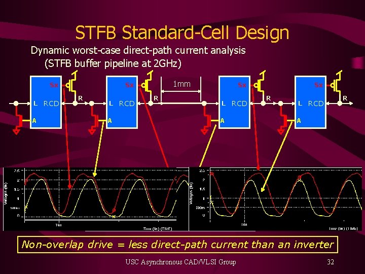
STFB Standard-Cell Design Dynamic worst-case direct-path current analysis (STFB buffer pipeline at 2 GHz) Sx L A RCD 1 mm Sx R L A RCD R Sx L RCD A Sx R L R RCD A TSMC 0. 25 mm, widths in mm and all lengths 0. 24 mm Non-overlap drive = less direct-path current than an inverter USC Asynchronous CAD/VLSI Group 32
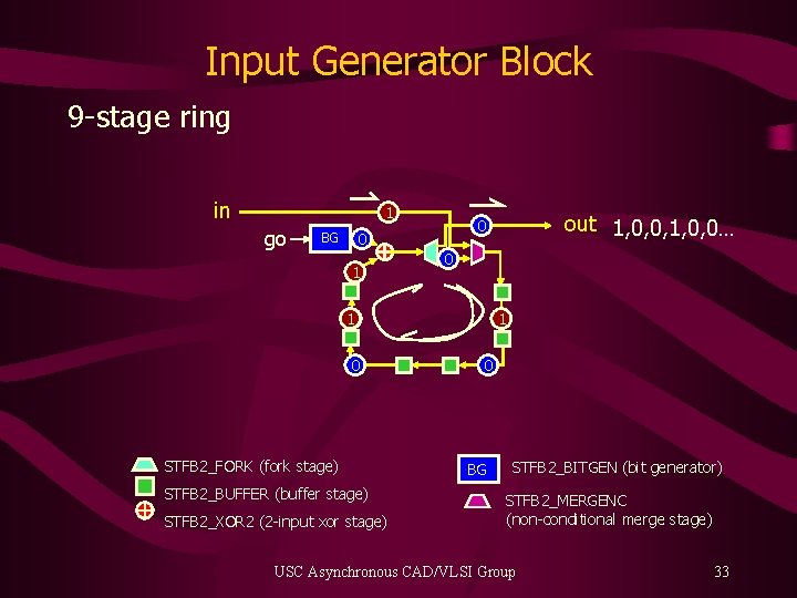
Input Generator Block 9 -stage ring in 1 go 1 0 10 0 STFB 2_FORK (fork stage) STFB 2_BUFFER (buffer stage) STFB 2_XOR 2 (2 -input xor stage) out 1, 0, 0, 1, 0, 0… 0 0 BG 1 0 BG STFB 2_BITGEN (bit generator) STFB 2_MERGENC (non-conditional merge stage) USC Asynchronous CAD/VLSI Group 33
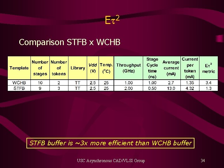
Et 2 Comparison STFB x WCHB STFB buffer is ~3 x more efficient than WCHB buffer USC Asynchronous CAD/VLSI Group 34
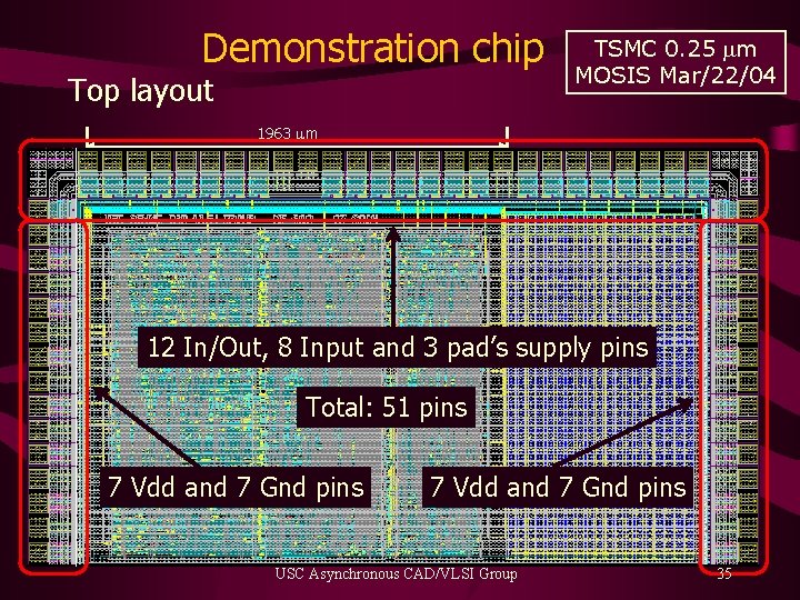
Demonstration chip Top layout TSMC 0. 25 mm MOSIS Mar/22/04 1963 mm 801 mm 663 mm INPUTGEN 129 BY 9 ADDER 64 1. 36 mm 2 105 k transistors 1. 3 A @ 1. 4 GHz 1. 13 mm 2 89 k transistors 1. 3 A @ 1. 4 GHz 499 mm SAMPLER 65 BY 1000 0. 85 mm 2 62 k transistors 0. 3 A @ 1. 4 GHz 12 In/Out, 8 Input and 3 pad’s supply pins 1700 mm Total: 51 pins 7 Vdd and 3. 3 mm 2 257 k transistors A @pins 1. 4 GHz 7 2. 9 Gnd 7 Vdd and 7 Gnd pins USC Asynchronous CAD/VLSI Group 35
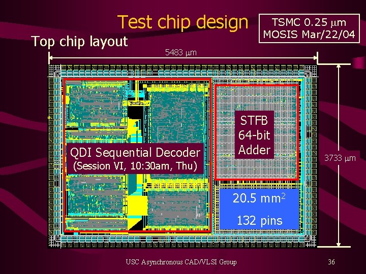
Test chip design Top chip layout TSMC 0. 25 mm MOSIS Mar/22/04 5483 mm STFB 64 -bit Adder QDI Sequential Decoder (Session VI, 10: 30 am, Thu) 3733 mm 20. 5 mm 2 132 pins USC Asynchronous CAD/VLSI Group 36
- Slides: 36