High efficiency system design with Infineon power discretes

![A short description of Cool. MOS™ Ron x A [Wmm 2] q High voltage A short description of Cool. MOS™ Ron x A [Wmm 2] q High voltage](https://slidetodoc.com/presentation_image_h2/2f24823fd636e7cf7153a20d2f86e665/image-6.jpg)


![Cool. MOS™ C 6/E 6 Portfolio 600 V TO-252 D-Pak [D] 3. 3 Ω Cool. MOS™ C 6/E 6 Portfolio 600 V TO-252 D-Pak [D] 3. 3 Ω](https://slidetodoc.com/presentation_image_h2/2f24823fd636e7cf7153a20d2f86e665/image-18.jpg)

- Slides: 52

High efficiency system design with Infineon power discretes -Infineon Cool. MOSTM, Opti. MOSTM, IGBT and Si. C diode Vincent Zeng(曾伟权) System application engineer Infineon Technologies China Weiquan. zeng@infineon. com

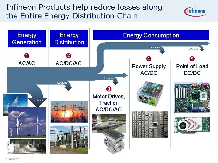
Infineon Products help reduce losses along the Entire Energy Distribution Chain Energy Generation Energy Distribution AC/AC AC/DC/AC Energy Consumption Losses Motor Drives, Traction AC/DC/AC ~10% 10. 02. 2010 Losses Power Supply AC/DC Point of Load DC/DC

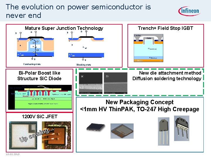
The evolution on power semiconductor is never end Mature Super Junction Technology G G S - n p+ pp n + n - n sub Trench+ Field Stop IGBT S p+ p n epi D Conducting state Bi-Polar Boost like Structure Si. C Diode n + sub D Blocking state New die attachment method Diffusion soldering technology New Packaging Concept <1 mm HV Thin. PAK, TO-247 High Creepage 1200 V Si. C JFET Up 10. 02. 2010 g… n i com

Content Cool. MOS technology Opti. MOS technology Trench. Stop IGBT technology Si. C diode technology 10. 02. 2010 Copyright © Infineon Technologies 2010. All rights reserved.

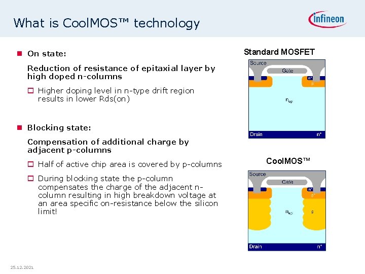
What is Cool. MOS™ technology On state: Standard MOSFET Reduction of resistance of epitaxial layer by high doped n-columns o Higher doping level in n-type drift region results in lower Rds(on) Blocking state: Compensation of additional charge by adjacent p-columns o Half of active chip area is covered by p-columns o During blocking state the p-column compensates the charge of the adjacent ncolumn resulting in high breakdown voltage at an area specific on-resistance below the silicon limit! 25. 12. 2021 Cool. MOS™
![A short description of Cool MOS Ron x A Wmm 2 q High voltage A short description of Cool. MOS™ Ron x A [Wmm 2] q High voltage](https://slidetodoc.com/presentation_image_h2/2f24823fd636e7cf7153a20d2f86e665/image-6.jpg)
A short description of Cool. MOS™ Ron x A [Wmm 2] q High voltage MOSFET in 500 V, 650 V, 800 V and 900 V Standard MOSFET Ron x A ~ V(BR)DSS 2, 4. . . 2, 6 q Offers a significant reduction of conduction and switching losses q Enables high power density and efficiency for superior power conversion systems New horizons for high voltage applications Cool. MOSTM q Best-in-class price/performance ratio Fig. : A near-linear relationship between Rds(on) and V(BR)DSS indicates the significant difference between Cool. MOS and conventional MOSFET Cool. MOSTM – Technology leader in high voltage MOSFETs 25. 12. 2021

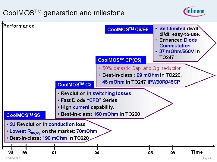
Cool. MOSTM generation and milestone Performance Cool. MOSTM C 6/E 6 Cool. MOSTM CP(C 5) • Self-limited dv/dt, di/dt, easy-to-use. • Enhanced Diode Commutation • 37 m. Ohm/650 V in TO 247 • 50% parastic Cap. and Qg. reduction • Best-in-class : 99 m. Ohm in TO 220, 45 m. Ohm in TO 247 IPW 60 R 045 CP Cool. MOSTM C 3 • Revolution in switching losses • Fast Diode “CFD” Series • High current capability. • Best-in-class: 160 m. Ohm in TO 220 Cool. MOSTM S 5 • SJ Revolution in conduction loss • Lowest Rds(on) on the market: 70 m. Ohm • Best-in-class: 190 m. Ohm in TO 220 98 10. 02. 2010 99 01 04 08 09 Time Page 7

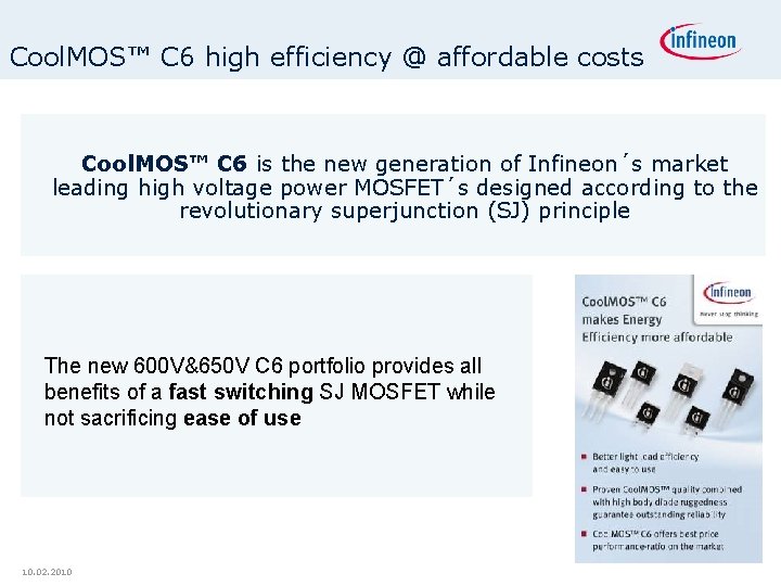
Cool. MOS™ C 6 high efficiency @ affordable costs Cool. MOS™ C 6 is the new generation of Infineon´s market leading high voltage power MOSFET´s designed according to the revolutionary superjunction (SJ) principle The new 600 V&650 V C 6 portfolio provides all benefits of a fast switching SJ MOSFET while not sacrificing ease of use 10. 02. 2010

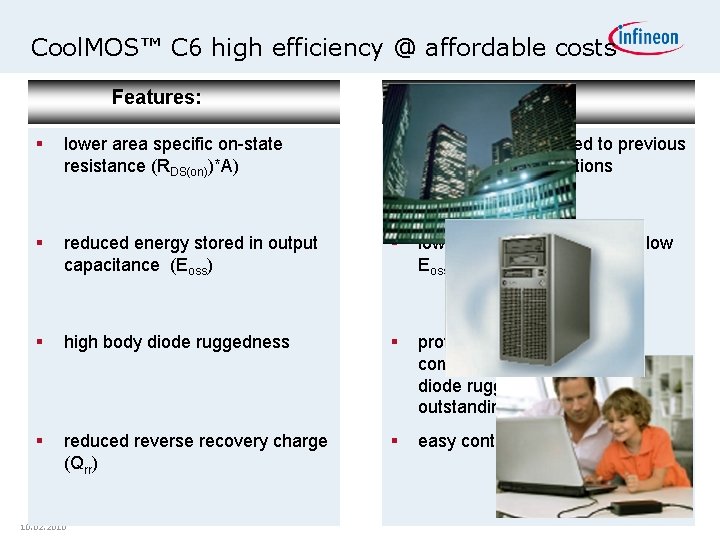
Cool. MOS™ C 6 high efficiency @ affordable costs Features: Benefits: § lower area specific on-state resistance (RDS(on))*A) § lower costs compared to previous Cool. MOS™ generations § reduced energy stored in output capacitance (Eoss) § low switching losses (due to low Eoss) § high body diode ruggedness § proven Cool. MOS™ quality combined with high body diode ruggedness guarantee outstanding reliability § reduced reverse recovery charge (Qrr) § easy control of switching behavior 10. 02. 2010

Cool. MOS C 6 reduced energy stored in output capacitance Cool. MOS™C 6 shows the best Figure-of-merit Ron ∗ Eoss 600 V Low energy stored in output capacitance make Cool. MOS™C 6 the right choice for hard switching applications. 650 V

Cool. MOS™ C 6 600 V efficiency measurement Efficiency comparison Cool. MOS C 6 versus C 3 Ease of use & good efficiency especially in light load conditions! 10. 02. 2010

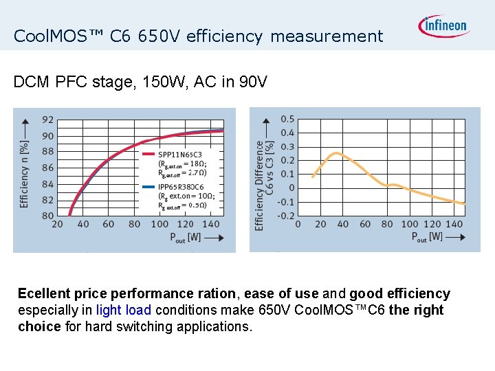
Cool. MOS™ C 6 650 V efficiency measurement DCM PFC stage, 150 W, AC in 90 V Ecellent price performance ration, ease of use and good efficiency especially in light load conditions make 650 V Cool. MOS™C 6 the right choice for hard switching applications.

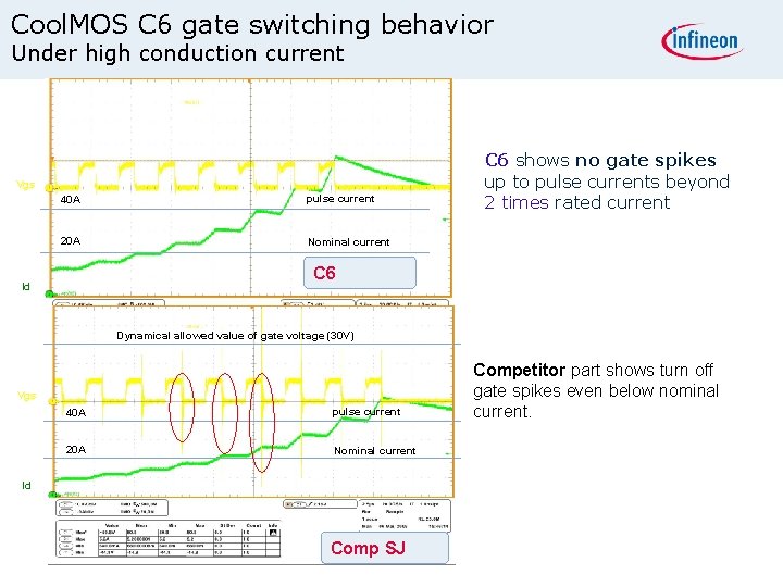
Cool. MOS C 6 gate switching behavior Under high conduction current Vgs 40 A pulse current 20 A Nominal current C 6 shows no gate spikes up to pulse currents beyond 2 times rated current C 6 Id Dynamical allowed value of gate voltage (30 V) Vgs 40 A pulse current 20 A Nominal current Id Comp SJ Competitor part shows turn off gate spikes even below nominal current.

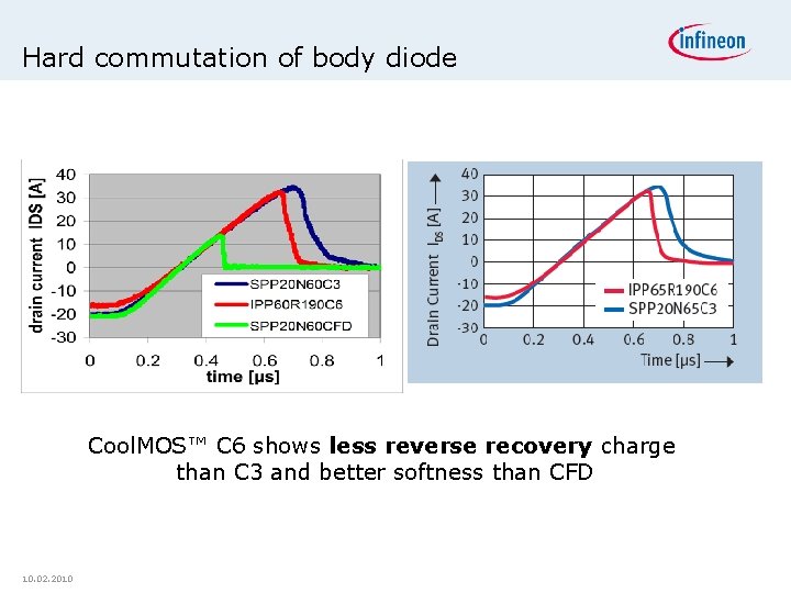
Hard commutation of body diode Cool. MOS™ C 6 shows less reverse recovery charge than C 3 and better softness than CFD 10. 02. 2010

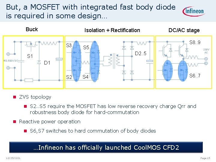
But, a MOSFET with integrated fast body diode is required in some design… Buck Isolation + Rectification S 3 S 8. . 9 S 5 230 V AC D 2. . 5 S 1 350. . 500 V DC DC/AC stage D 1 S 2 S 4 S 6. . 7 ZVS topology S 2. . S 5 require the MOSFET has low reverse recovery charge Qrr and robustness body diode for hard-commutation Reactive power operation S 6, S 7 switches to hard commutation of body diodes …Infineon has officially launched Cool. MOS CFD 2 12/25/2021 Page 15

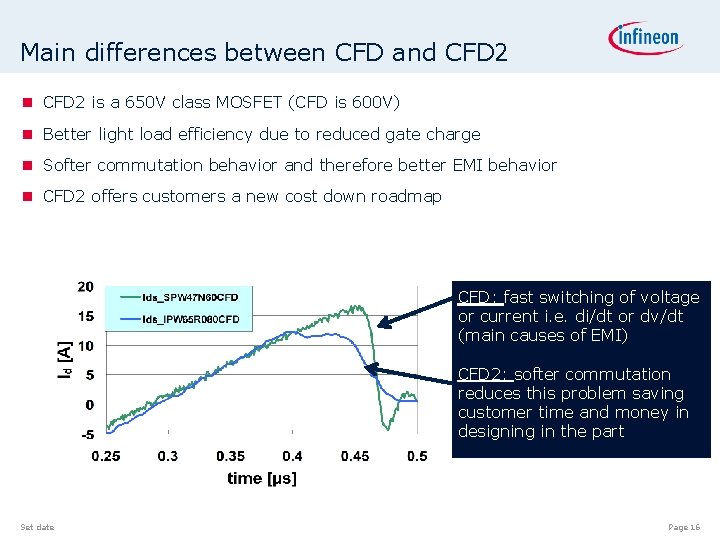
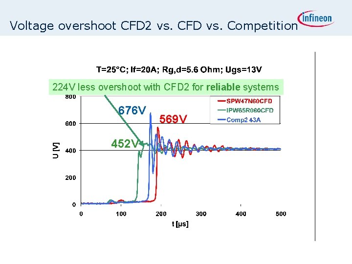
Main differences between CFD and CFD 2 is a 650 V class MOSFET (CFD is 600 V) Better light load efficiency due to reduced gate charge Softer commutation behavior and therefore better EMI behavior CFD 2 offers customers a new cost down roadmap CFD: fast switching of voltage or current i. e. di/dt or dv/dt (main causes of EMI) CFD 2: softer commutation reduces this problem saving customer time and money in designing in the part Set date Page 16

Voltage overshoot CFD 2 vs. CFD vs. Competition 224 V less overshoot with CFD 2 for reliable systems 676 V 452 V 569 V
![Cool MOS C 6E 6 Portfolio 600 V TO252 DPak D 3 3 Ω Cool. MOS™ C 6/E 6 Portfolio 600 V TO-252 D-Pak [D] 3. 3 Ω](https://slidetodoc.com/presentation_image_h2/2f24823fd636e7cf7153a20d2f86e665/image-18.jpg)
Cool. MOS™ C 6/E 6 Portfolio 600 V TO-252 D-Pak [D] 3. 3 Ω 1. 8 A IPD 60 R 3 k 3 C 6 2Ω 2. 5 A IPD 60 R 2 k 0 C 6 1. 4 Ω 3. 2 A IPD 60 R 1 k 4 C 6 0. 95 Ω 4. 5 A IPD 60 R 950 C 6 0. 75 Ω 6. 2 A IPD 60 R 750 E 6 0. 6 Ω 7. 3 A IPD 60 R 600 E 6 0. 52 Ω 8 A TO-263 D²PAK [B] TO-220 [P] TO-220 Fullpak [A] TO-262 I²-PAK [I] TO-247 [W] IPP 60 R 1 k 4 C 6 IPB 60 R 950 C 6 IPP 60 R 950 C 6 IPA 60 R 950 C 6 IPP 60 R 750 E 6 IPA 60 R 750 E 6 IPP 60 R 600 E 6 IPA 60 R 600 E 6 IPD 60 R 520 C 6 IPP 60 R 520 E 6 IPA 60 R 520 E 6 0. 45 Ω 9. 5 A IPD 60 R 450 E 6 IPP 60 R 450 E 6 IPA 60 R 450 E 6 0. 38 Ω 11 A IPD 60 R 380 C 6 IPB 60 R 380 C 6 IPP 60 R 380 E 6 IPA 60 R 380 E 6 IPI 60 R 380 C 6 0. 28 Ω 15 A IPB 60 R 280 C 6 IPP 60 R 280 E 6 IPA 60 R 280 E 6 IPI 60 R 280 C 6 IPW 60 R 280 E 6 0. 19 Ω 20 A IPB 60 R 190 C 6 IPP 60 R 190 E 6 IPA 60 R 190 E 6 IPI 60 R 190 C 6 IPW 60 R 190 E 6 0. 16 Ω 24 A IPB 60 R 160 C 6 IPP 60 R 160 C 6 IPA 60 R 160 C 6 IPW 60 R 160 C 6 IPP 60 R 125 C 6 IPA 60 R 125 C 6 IPW 60 R 125 C 6 IPP 60 R 099 C 6 IPA 60 R 099 C 6 IPW 60 R 099 C 6 IPB 60 R 600 C 6 0. 125 Ω 30 A 0. 099 Ω 35 A IPB 60 R 099 C 6 0. 07 Ω 47 A IPW 60 R 070 C 6 0. 041 Ω 77 A IPW 60 R 041 C 6

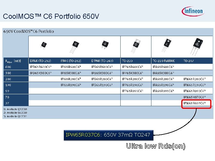
Cool. MOS™ C 6 Portfolio 650 V IPW 65 R 037 C 6: 650 V 37 mΩ TO 247 Ultra low Rds(on)

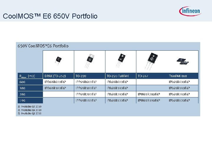
Cool. MOS™ E 6 650 V Portfolio

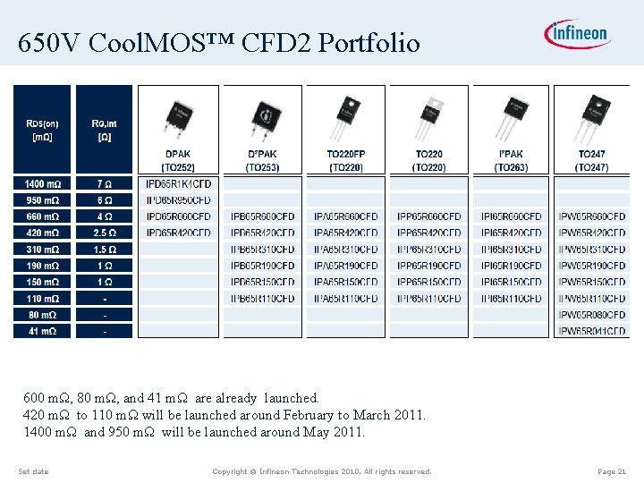
650 V Cool. MOS™ CFD 2 Portfolio 600 mΩ, 80 mΩ, and 41 mΩ are already launched. 420 mΩ to 110 mΩ will be launched around February to March 2011. 1400 mΩ and 950 mΩ will be launched around May 2011. Set date Copyright © Infineon Technologies 2010. All rights reserved. Page 21

Content Cool. MOS technology Opti. MOS technology Trench. Stop IGBT technology Si. C diode technology 10. 02. 2010 Copyright © Infineon Technologies 2010. All rights reserved.

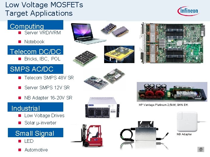
Low Voltage MOSFETs Target Applications Computing Server VRD/VRM Notebook Telecom DC/DC Bricks, IBC, POL SMPS AC/DC Telecom SMPS 48 V SR Server SMPS 12 V SR NB Adapter 16 -20 V SR Industrial HP Vantage Platinum 2, 5 k. W; 94% Eff. Low Voltage Drives Solar µ-inverter Small Signal LED Automotive NB Adapter

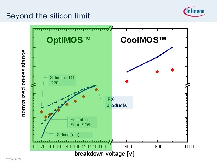
Beyond the silicon limit normalized on-resistance Opti. MOS™ Cool. MOS™ Si-limit in TO -220 IFXproducts Si-limit in Super. SO 8 Si-limit (die) 0 20 40 60 80 100 120 140 160 600 breakdown voltage [V] 2021/12/25 800 1000

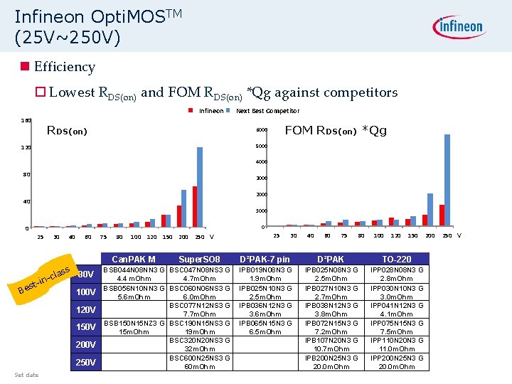
Infineon Opti. MOSTM (25 V~250 V) Efficiency o Lowest RDS(on) and FOM RDS(on) *Qg against competitors Infineon 160 RDS(on) Next Best Competitor FOM RDS(on) *Qg 6000 5000 120 4000 80 3000 2000 40 1000 0 0 25 30 40 60 75 80 100 120 150 200 250 V Can. PAK M ass -cl n i st Be 80 V 100 V 120 V 150 V 200 V 250 V Set date Super. SO 8 BSB 044 N 08 NN 3 G BSC 047 N 08 NS 3 G 4. 4 m. Ohm 4. 7 m. Ohm BSB 056 N 10 NN 3 G BSC 060 N 06 NS 3 G 5. 6 m. Ohm 6. 0 m. Ohm BSC 077 N 12 NS 3 G 7. 7 m. Ohm BSB 150 N 15 NZ 3 G BSC 190 N 15 NS 3 G 15 m. Ohm 19 m. Ohm BSC 320 N 20 NS 3 G 32 m. Ohm BSC 600 N 25 NS 3 G 60 m. Ohm 25 30 40 60 75 80 100 120 150 D²PAK-7 pin D²PAK TO-220 IPB 019 N 08 N 3 G 1. 9 m. Ohm IPB 025 N 10 N 3 G 2. 5 m. Ohm IPB 036 N 12 N 3 G 3. 6 m. Ohm IPB 065 N 15 N 3 G 6. 5 m. Ohm IPB 025 N 08 N 3 G 2. 5 m. Ohm IPB 027 N 10 N 3 G 2. 7 m. Ohm IPB 038 N 12 N 3 G 3. 8 m. Ohm IPB 072 N 15 N 3 G 7. 2 m. Ohm IPB 107 N 20 N 3 G 10. 7 m. Ohm IPB 200 N 25 N 3 G 20. 0 m. Ohm IPP 028 N 08 N 3 G 2. 8 m. Ohm IPP 030 N 10 N 3 G 3. 0 m. Ohm IPP 041 N 12 N 3 G 4. 1 m. Ohm IPP 075 N 15 N 3 G 7. 5 m. Ohm IPP 110 N 20 N 3 G 11. 0 m. Ohm IPP 200 N 25 N 3 G 20. 0 m. Ohm 200 250 V

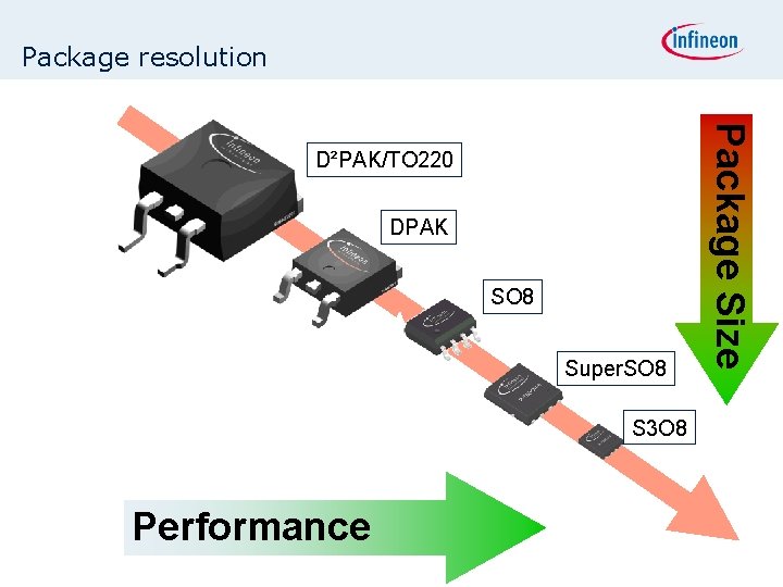
Package resolution DPAK SO 8 Super. SO 8 S 3 O 8 Performance Package Size D²PAK/TO 220

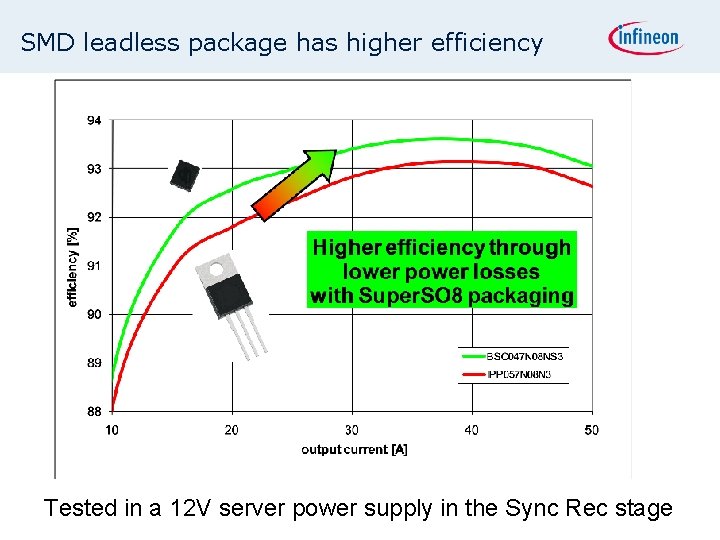
SMD leadless package has higher efficiency Tested in a 12 V server power supply in the Sync Rec stage

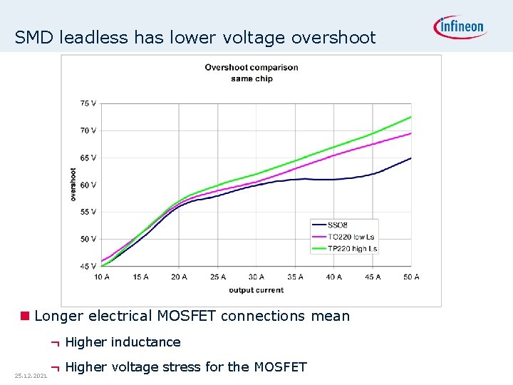
SMD leadless has lower voltage overshoot Longer electrical MOSFET connections mean ¬ Higher inductance 25. 12. 2021 ¬ Higher voltage stress for the MOSFET

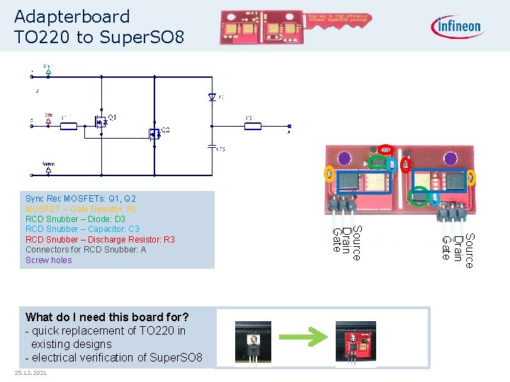
Adapterboard TO 220 to Super. SO 8 25. 12. 2021 Source Drain Gate What do I need this board for? - quick replacement of TO 220 in existing designs - electrical verification of Super. SO 8 Source Drain Gate Sync Rec MOSFETs: Q 1, Q 2 MOSFET – Gate Resistor: R 1 RCD Snubber – Diode: D 3 RCD Snubber – Capacitor: C 3 RCD Snubber – Discharge Resistor: R 3 Connectors for RCD Snubber: A Screw holes

Content Cool. MOS technology Opti. MOS technology Trench. Stop IGBT technology Si. C diode technology 10. 02. 2010 Copyright © Infineon Technologies 2010. All rights reserved.

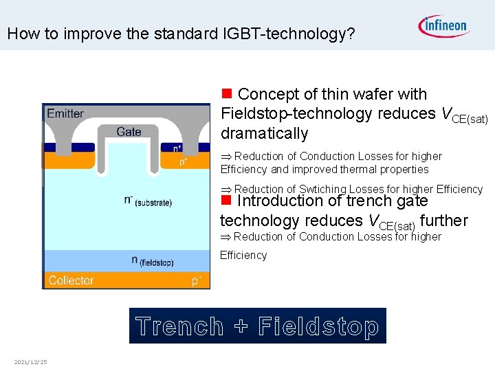
How to improve the standard IGBT-technology? Concept of thin wafer with Fieldstop-technology reduces VCE(sat) dramatically Reduction of Conduction Losses for higher Efficiency and improved thermal properties Reduction of Swtiching Losses for higher Efficiency Introduction of trench gate technology reduces VCE(sat) further Reduction of Conduction Losses for higher n (fieldstop) Efficiency Trench + Fieldstop 2021/12/25

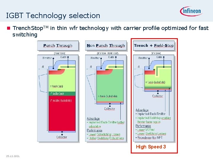
IGBT Technology selection Trench. Stop. TM in thin wfr technology with carrier profile optimized for fast switching High Speed 3 25. 12. 2021

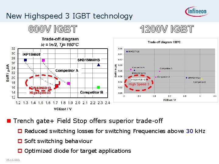
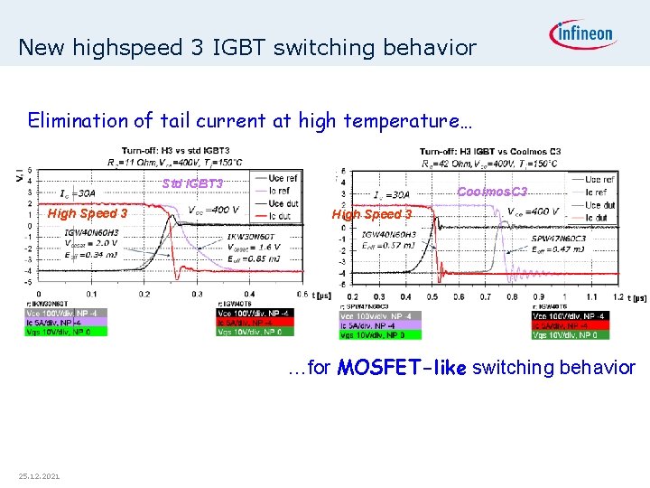
New Highspeed 3 IGBT technology 600 V IGBT 1200 V IGBT High Speed 3 Trench gate+ Field Stop offers superior trade-off p Reduced switching losses for switching Frequencies above 30 k. Hz p Soft switching behaviour p Optimized diode for target applications 25. 12. 2021 Applikationsbewertung

New highspeed 3 IGBT switching behavior Elimination of tail current at high temperature… Std IGBT 3 High Speed 3 Coolmos. C 3 High Speed 3 …for MOSFET-like switching behavior 25. 12. 2021

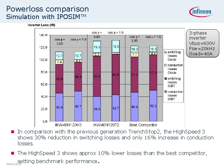
Powerloss comparison Simulation with IPOSIMTM 3 -phase inverter Vbus=600 V Fsw=20 k. Hz Iload=40 A In comparison with the previous generation Trench. Stop 2, the High. Speed 3 shows 30% reduction in switching losses and only 16% increase in conduction losses. The High. Speed 3 shows approx 10% lower losses than the best competitor, setting benchmark performance. 2021/12/25

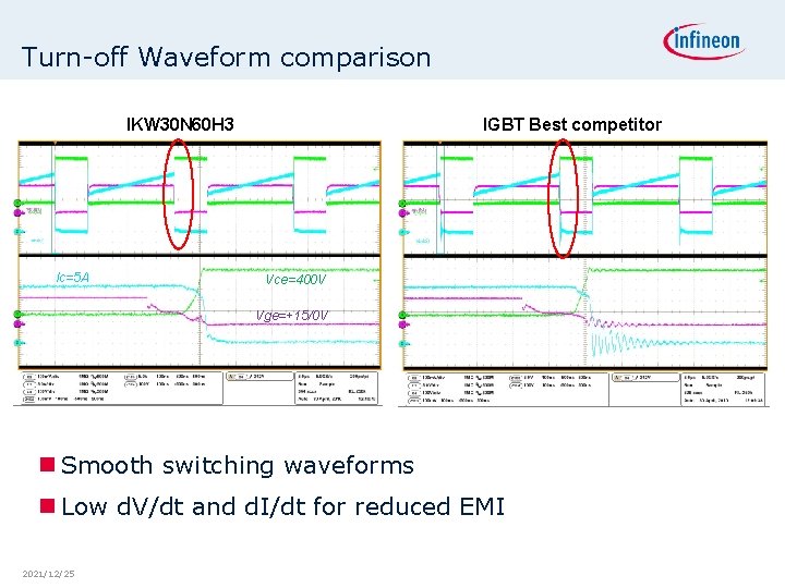
Turn-off Waveform comparison IGBT Best competitor IKW 30 N 60 H 3 Ic=5 A Vce=400 V Vge=+15/0 V Smooth switching waveforms Low d. V/dt and d. I/dt for reduced EMI 2021/12/25

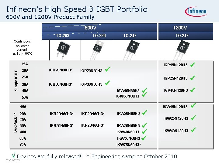
Infineon’s High Speed 3 IGBT Portfolio 600 V and 1200 V Product Family 600 V TO-263 1200 V TO-220 TO-247 Continuous collector current at T C =100°C 15 A Single IGBT 20 A IGB 20 N 60 H 3* IGP 20 N 60 H 3 25 A 30 A IGB 30 N 60 H 3* IGP 30 N 60 H 3 40 A IGW 40 N 60 H 3 IGW 50 N 60 H 3 50 A Duo. Pack ™ 15 A 20 A IKB 20 N 60 H 3* IKP 20 N 60 H 3* IKW 20 N 60 H 3 25 A 30 A IKB 30 N 60 H 3* IKP 20 N 60 H 3* 40 A 50 A 75 A √ Devices are fully released! 25. 12. 2021 IKW 40 N 60 H 3 IKW 50 N 60 H 3 IGP 15 N 120 H 3 IGP 25 N 120 H 3 IGP 40 N 120 H 3 IKW 15 N 120 H 3 IKW 25 N 120 H 3 IKW 40 N 120 H 3 IKW 30 N 60 H 3 IKW 75 N 60 H 3* * Engineering samples October 2010

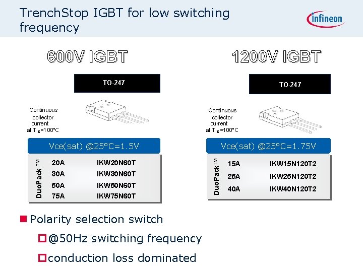
Trench. Stop IGBT for low switching frequency 600 V IGBT 1200 V IGBT TO-247 Continuous collector current at T C =100°C 20 A IKW 20 N 60 T 30 A IKW 30 N 60 T 50 A IKW 50 N 60 T 75 A IKW 75 N 60 T Polarity selection switch p @50 Hz switching frequency p conduction loss dominated Vce(sat) @25°C=1. 75 V Duo. Pack™ Duo. Pack ™ Vce(sat) @25°C=1. 5 V 15 A IKW 15 N 120 T 2 25 A IKW 25 N 120 T 2 40 A IKW 40 N 120 T 2

Content Cool. MOS technology Opti. MOS technology Trench. Stop IGBT technology Si. C diode technology 10. 02. 2010 Copyright © Infineon Technologies 2010. All rights reserved.

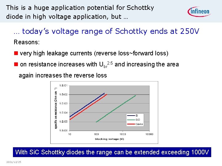
This is a huge application potential for Schottky diode in high voltage application, but … … today’s voltage range of Schottky ends at 250 V Reasons: very high leakage currents (reverse loss~forward loss) on resistance increases with Ubr 2. 5 and increasing the area again increases the reverse loss With Si. C Schottky diodes the range can be extended exceeding 1000 V 2021/12/25

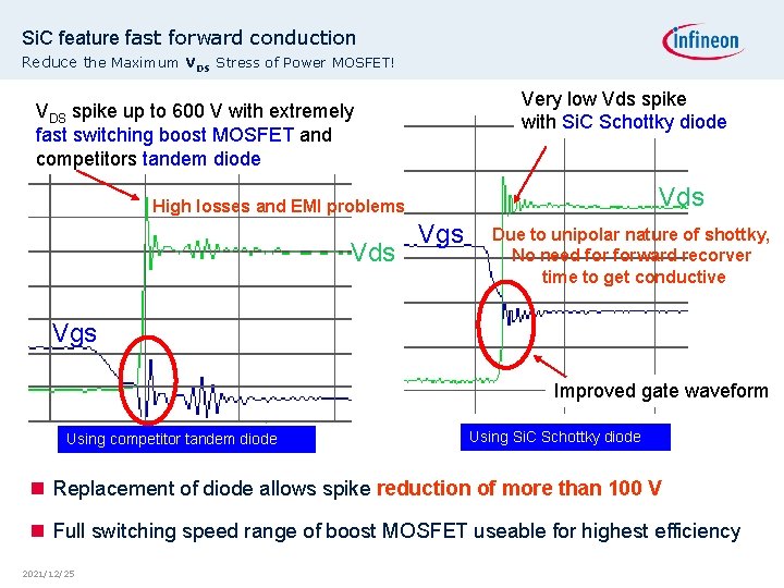
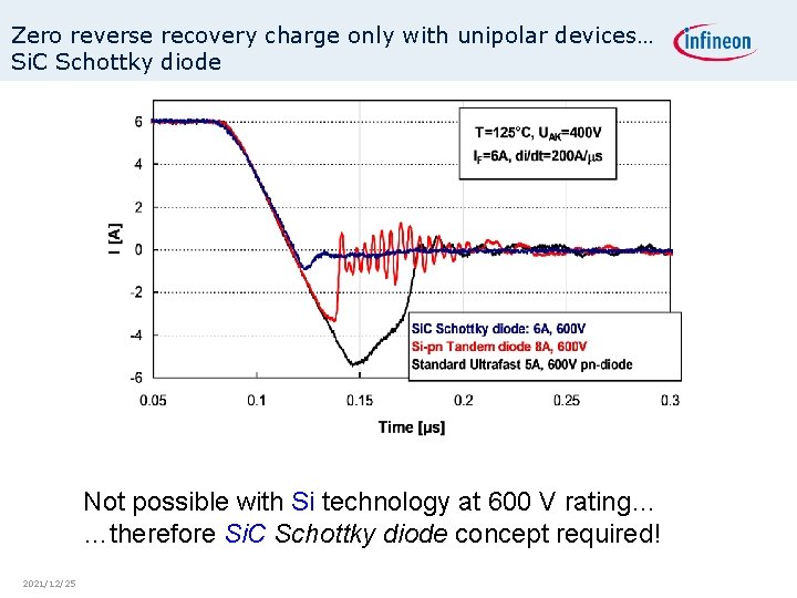
Si. C feature fast forward conduction Reduce the Maximum VDS Stress of Power MOSFET! Very low Vds spike with Si. C Schottky diode VDS spike up to 600 V with extremely fast switching boost MOSFET and competitors tandem diode Vds High losses and EMI problems Vds Vgs Due to unipolar nature of shottky, No need forward recorver time to get conductive Vgs Improved gate waveform Using competitor tandem diode Using Si. C Schottky diode Replacement of diode allows spike reduction of more than 100 V Full switching speed range of boost MOSFET useable for highest efficiency 2021/12/25

Zero reverse recovery charge only with unipolar devices… Si. C Schottky diode Not possible with Si technology at 600 V rating… …therefore Si. C Schottky diode concept required! 2021/12/25

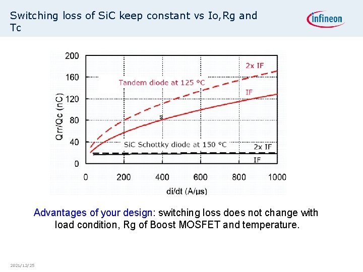
Switching loss of Si. C keep constant vs Io, Rg and Tc Advantages of your design: switching loss does not change with load condition, Rg of Boost MOSFET and temperature. 2021/12/25

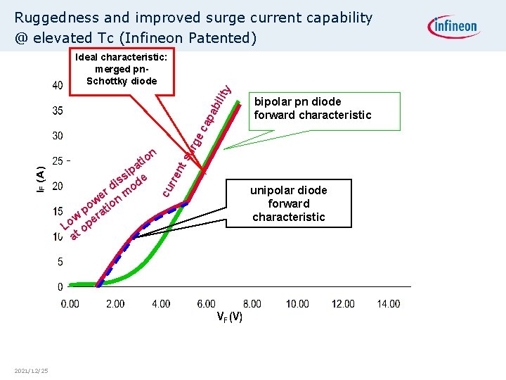
Ruggedness and improved surge current capability @ elevated Tc (Infineon Patented) bipolar pn diode forward characteristic 2021/12/25 rre nt pa i s is ode d er n m w o po rati w e Lo op at cu n it o su rg ec ap ab il ity Ideal characteristic: merged pn. Schottky diode unipolar diode forward characteristic

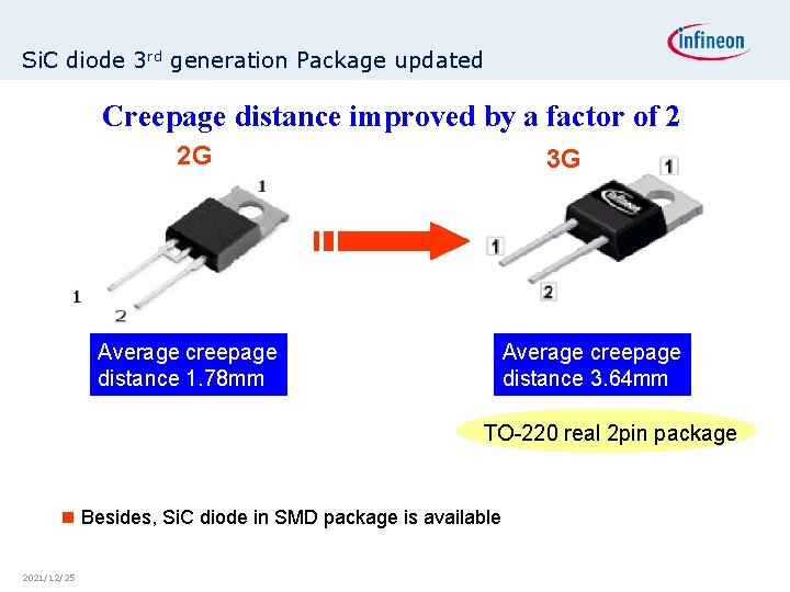
Si. C diode 3 rd generation Package updated Creepage distance improved by a factor of 2 2 G 3 G Average creepage distance 1. 78 mm Average creepage distance 3. 64 mm TO-220 real 2 pin package Besides, Si. C diode in SMD package is available 2021/12/25

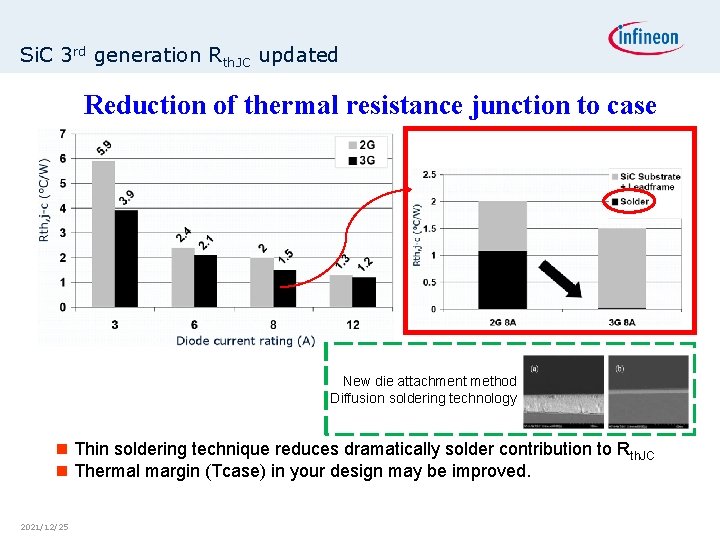
Si. C 3 rd generation Rth. JC updated Reduction of thermal resistance junction to case New die attachment method Diffusion soldering technology Thin soldering technique reduces dramatically solder contribution to Rth. JC Thermal margin (Tcase) in your design may be improved. 2021/12/25

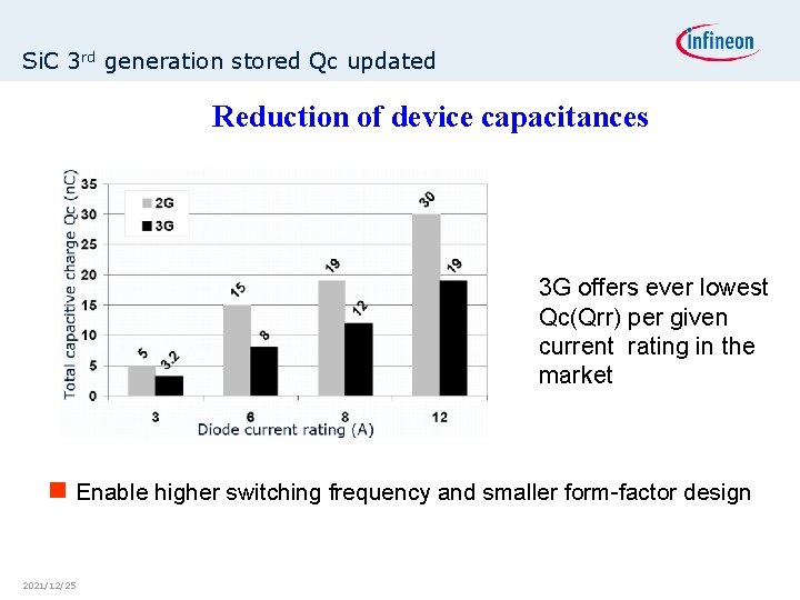
Si. C 3 rd generation stored Qc updated Reduction of device capacitances 3 G offers ever lowest Qc(Qrr) per given current rating in the market Enable higher switching frequency and smaller form-factor design 2021/12/25

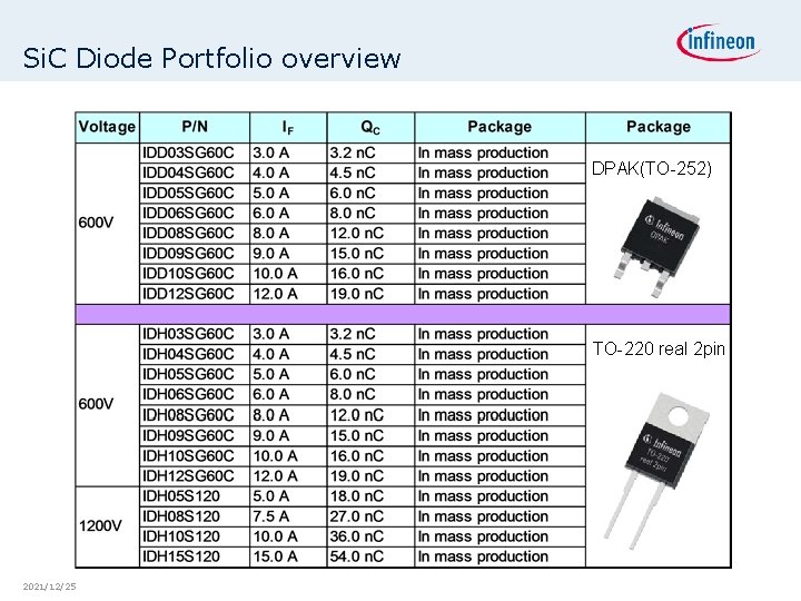
Si. C Diode Portfolio overview DPAK(TO-252) TO-220 real 2 pin 2021/12/25

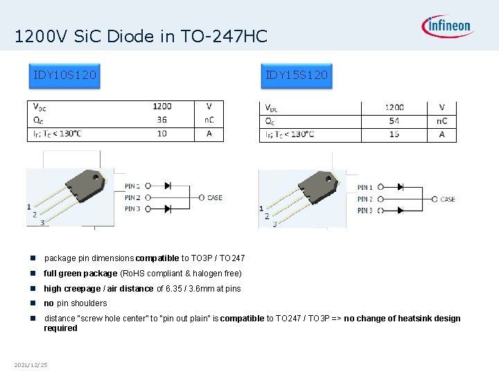
1200 V Si. C Diode in TO-247 HC IDY 10 S 120 IDY 15 S 120 package pin dimensions compatible to TO 3 P / TO 247 full green package (Ro. HS compliant & halogen free) high creepage / air distance of 6. 35 / 3. 6 mm at pins no pin shoulders distance “screw hole center” to “pin out plain” is compatible to TO 247 / TO 3 P => no change of heatsink design required 2021/12/25

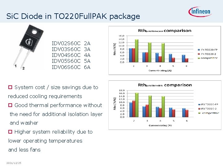
Si. C Diode in TO 220 Full. PAK package IDV 02 S 60 C IDV 03 S 60 C IDV 04 S 60 C IDV 05 S 60 C IDV 06 S 60 C 2 A 3 A 4 A 5 A 6 A p System cost / size savings due to reduced cooling requirements p Good thermal performance without the need for additional isolation layer and washer p Higher system reliability due to lower operating temperatures and less fans 2021/12/25

Summary Explore our website, put us to the test and see why Infineon's power semiconductors lead to your Superior Solutions. o Cool. MOS (500 V~900 V) ¬ www. infineon. com/Cool. MOS o Opti. MOS (25 V~250 V) ¬ www. infineon. com/Opti. MOS o IGBT ¬ www. infineon. com/IGBT o Si. C diode (600 V/1200 V) ¬ www. infineon. com/Si. C 25. 12. 2021
