High efficiency Si solar cells Recombination and generation
High efficiency Si solar cells Recombination and generation currents, Back Contact solar cells Prof. C. S. Solanki Department of Energy Science and Engineering IIT Bombay
Generation and Recombination Currents 12/29/2021 © IIT Bombay, C. S. Solanki Advanced Concepts in Solar Photovoltaic Technologies 2
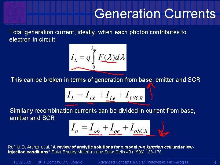
Generation Currents Total generation current, ideally, when each photon contributes to electron in circuit This can be broken in terms of generation from base, emitter and SCR Similarly recombination currents can be divided in current from base, emitter and SCR Ref: M. D. Archer et al, “A review of analytic solutions for a model p-n junction cell under lowinjection conditions” Solar Energy Materials and Solar Cells 40 (1996) 133 -176, 12/29/2021 © IIT Bombay, C. S. Solanki Advanced Concepts in Solar Photovoltaic Technologies 3
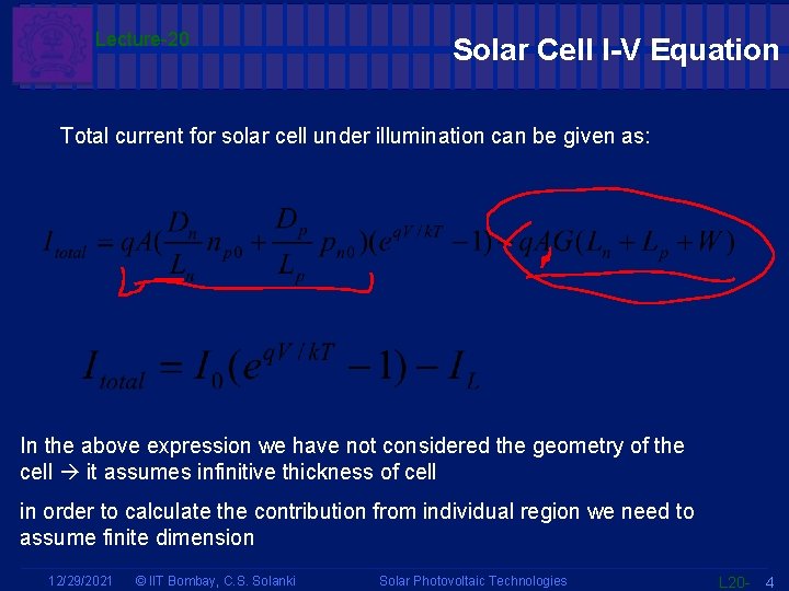
Lecture-20 Solar Cell I-V Equation Total current for solar cell under illumination can be given as: In the above expression we have not considered the geometry of the cell it assumes infinitive thickness of cell in order to calculate the contribution from individual region we need to assume finite dimension 12/29/2021 © IIT Bombay, C. S. Solanki Solar Photovoltaic Technologies L 20 - 4
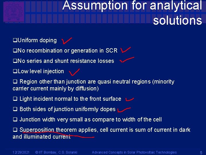
Assumption for analytical solutions q. Uniform doping q. No recombination or generation in SCR q. No series and shunt resistance losses q. Low level injection q Region other than junction are quasi neutral regions (minority carrier current mainly by diffusion) q Light incident normal to the front surface q Both sides of junction uniformly dopes q Junction width very small as compare to width of the cell q Superposition theorem applies, cell current is sum of current in dark and illuminated current 12/29/2021 © IIT Bombay, C. S. Solanki Advanced Concepts in Solar Photovoltaic Technologies 5
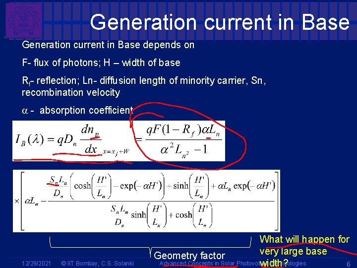
= Generation current in Base depends on F- flux of photons; H – width of base Rf- reflection; Ln- diffusion length of minority carrier, Sn, recombination velocity - absorption coefficient 12/29/2021 © IIT Bombay, C. S. Solanki What will happen for very large base Geometry factor Advanced Concepts in Solar Photovoltaic Technologies width? 6
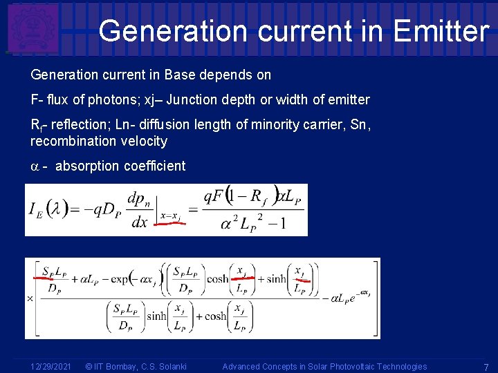
Generation current in Emitter = Generation current in Base depends on F- flux of photons; xj– Junction depth or width of emitter Rf- reflection; Ln- diffusion length of minority carrier, Sn, recombination velocity - absorption coefficient 12/29/2021 © IIT Bombay, C. S. Solanki Advanced Concepts in Solar Photovoltaic Technologies 7
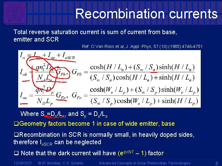
Recombination currents Total reverse saturation current is sum of current from base, emitter and SCR Ref: O Van Ross et al, J. Appl. Phys, 57 (10) (1985) 4746 -4751 Where Sn=Dn/Ln, and Sp = Dp/Lp q. Geometry factors become 1 in case of wide emitter, base q. Recombination in SCR is normally small, in heavily doped sides, therefore Io. SCR can be neglected q Note that the dark current will have (eq. V/k. T – 1) factor 12/29/2021 © IIT Bombay, C. S. Solanki Advanced Concepts in Solar Photovoltaic Technologies 8
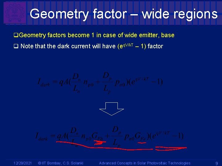
Geometry factor – wide regions q. Geometry factors become 1 in case of wide emitter, base q Note that the dark current will have (eq. V/k. T – 1) factor 12/29/2021 © IIT Bombay, C. S. Solanki Advanced Concepts in Solar Photovoltaic Technologies 9
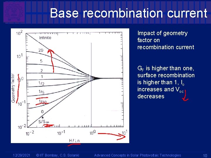
Base recombination current Impact of geometry factor on recombination current GF is higher than one, surface recombination is higher than 1, Io increases and Voc decreases 12/29/2021 © IIT Bombay, C. S. Solanki Advanced Concepts in Solar Photovoltaic Technologies 10

Schockley-Read-Hall model Dynamics of this recombination process in described by Schockley. Read-Hall (SRH) theory Single trap level Et Where are the constant related with the density and activity of the traps and is called minority carrier lifetime and n 1 and p 1 is given as: 12/29/2021 © IIT Bombay, C. S. Solanki 11
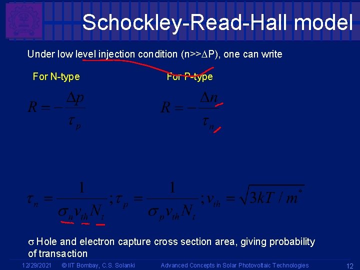
Schockley-Read-Hall model Under low level injection condition (n>> P), one can write For N-type For P-type Hole and electron capture cross section area, giving probability of transaction 12/29/2021 © IIT Bombay, C. S. Solanki Advanced Concepts in Solar Photovoltaic Technologies 12
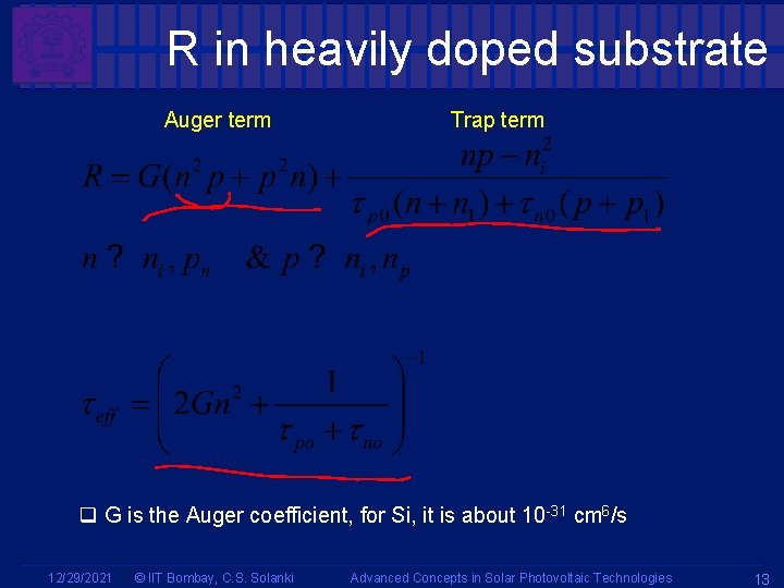
R in heavily doped substrate Auger term Trap term q G is the Auger coefficient, for Si, it is about 10 -31 cm 6/s 12/29/2021 © IIT Bombay, C. S. Solanki Advanced Concepts in Solar Photovoltaic Technologies 13
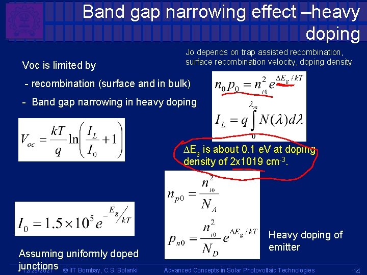
Band gap narrowing effect –heavy doping Voc is limited by Jo depends on trap assisted recombination, surface recombination velocity, doping density - recombination (surface and in bulk) - Band gap narrowing in heavy doping Eg is about 0. 1 e. V at doping density of 2 x 1019 cm-3. Assuming uniformly doped junctions 12/29/2021 © IIT Bombay, C. S. Solanki Heavy doping of emitter Advanced Concepts in Solar Photovoltaic Technologies 14
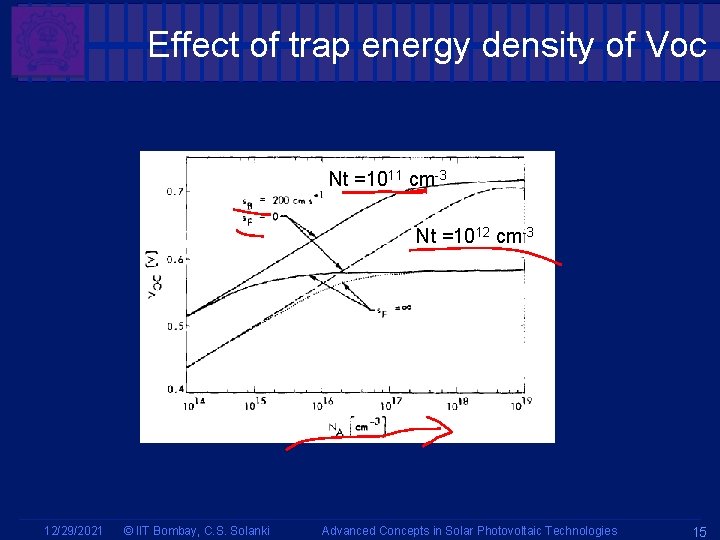
Effect of trap energy density of Voc Nt =1011 cm-3 Nt =1012 cm-3 12/29/2021 © IIT Bombay, C. S. Solanki Advanced Concepts in Solar Photovoltaic Technologies 15
Back Contact Solar Cells 12/29/2021 © IIT Bombay, C. S. Solanki Advanced Concepts in Solar Photovoltaic Technologies 16
Back contact solar cell In Back contact solar cells the idea is to bring both the contact at the rear side of the cell Why at rear side contacts? No metal coverage at front side, hence no shadowing losses higher cell performance No limitation on metal coverage at back side, series resistance can be lower Both contact at back provides simpler cell interconnection Higher packing density of cells in modules in possible 12/29/2021 © IIT Bombay, C. S. Solanki Advanced Concepts in Solar Photovoltaic Technologies 17
Types of back contact cells There are three categories of back contact solar cells q. Back-junction (BJ), q Emitter wrap through (EWT) and q Metallization wrap-through (MWT), A fourth type, novel approach for back contact solar cells is being developed at IITB 12/29/2021 © IIT Bombay, C. S. Solanki Advanced Concepts in Solar Photovoltaic Technologies 18
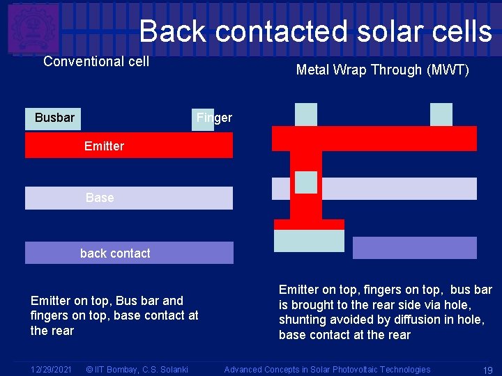
Back contacted solar cells Conventional cell Busbar Metal Wrap Through (MWT) Finger Emitter Base back contact Emitter on top, Bus bar and fingers on top, base contact at the rear 12/29/2021 © IIT Bombay, C. S. Solanki Emitter on top, fingers on top, bus bar is brought to the rear side via hole, shunting avoided by diffusion in hole, base contact at the rear Advanced Concepts in Solar Photovoltaic Technologies 19
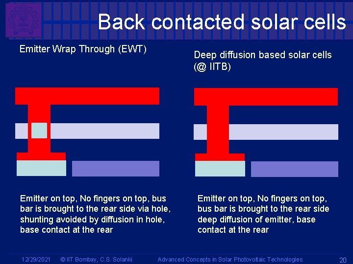
Back contacted solar cells Emitter Wrap Through (EWT) Deep diffusion based solar cells (@ IITB) Emitter on top, No fingers on top, bus bar is brought to the rear side via hole, shunting avoided by diffusion in hole, base contact at the rear 12/29/2021 © IIT Bombay, C. S. Solanki Emitter on top, No fingers on top, bus bar is brought to the rear side deep diffusion of emitter, base contact at the rear Advanced Concepts in Solar Photovoltaic Technologies 20
Back contacted solar cells Back contacted cells can be further be classified as: q Rear junction solar cells q Front junction solar cells References: Emmanuel Van Kerschaver et al, “Back contact solar cells” A review” PROGRESS IN PHOTOVOLTAICS: RESEARCH AND APPLICATIONS, Prog. Photovolt: Res. Appl. , 14 (2006) 107– 123 J. Dicker et al, “Analysis of one-sun monocrystalline rear-contacted silicon solar cells with efficiencies of 22. 1% “, Journal of Applied Physics Letters, 91 (2002) 4335 -4343 12/29/2021 © IIT Bombay, C. S. Solanki Advanced Concepts in Solar Photovoltaic Technologies 21
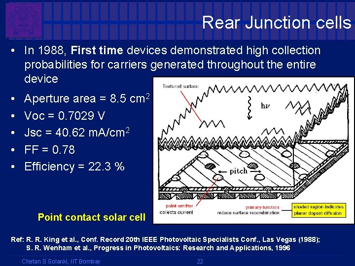
Rear Junction cells • In 1988, First time devices demonstrated high collection probabilities for carriers generated throughout the entire device • • • Aperture area = 8. 5 cm 2 Voc = 0. 7029 V Jsc = 40. 62 m. A/cm 2 FF = 0. 78 Efficiency = 22. 3 % Point contact solar cell Ref: R. R. King et al. , Conf. Record 20 th IEEE Photovoltaic Specialists Conf. , Las Vegas (1988); S. R. Wenham et al. , Progress in Photovoltaics: Research and Applications, 1996 Chetan S Solanki, IIT Bombay 22
Advantages of rear junction cells In conventional solar cells front contact design in a compromise between front optical design (low shadow, low reflection) and electrical design (low contact resistance) In back contact cells q Electrical design and optical design can be done independently low shadowing loss, low resistive loss q Current does not flow lateral in emitter, no trade-off for series resistance rear junction can be optimized for low saturation currents q Cell can be used for concentrator applications as well as terrestrial applications q Additionally, Interconnection of cells in module become easier 12/29/2021 © IIT Bombay, C. S. Solanki Advanced Concepts in Solar Photovoltaic Technologies 23
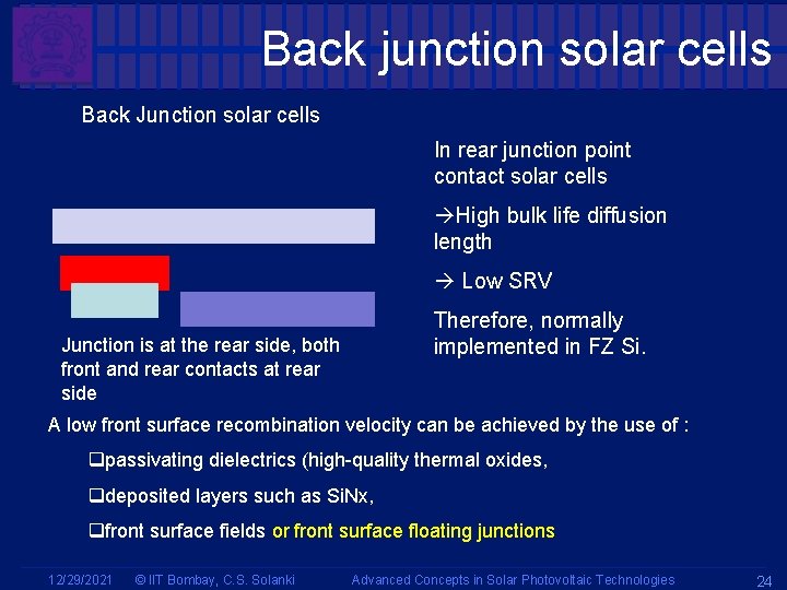
Back junction solar cells Back Junction solar cells In rear junction point contact solar cells High bulk life diffusion length Low SRV Therefore, normally implemented in FZ Si. Junction is at the rear side, both front and rear contacts at rear side A low front surface recombination velocity can be achieved by the use of : qpassivating dielectrics (high-quality thermal oxides, qdeposited layers such as Si. Nx, qfront surface fields or front surface floating junctions 12/29/2021 © IIT Bombay, C. S. Solanki Advanced Concepts in Solar Photovoltaic Technologies 24
Floating junction for surface passivation In case of rear junction solar cells, the front surface passivation is very important, obtaining excellent passivation on textured surface is difficult times larger surface area, exposure to 111 plane Floating junction are non-current collecting junctions q. Front surface diffusion repels minority carriers from front surface q. The function of the floating junction to passivate surface and not to collect current q. Jo can be made lower, sheet resistance of junction is not important For concentrator cell applications lowering series resistance using back contact cell is main issue, In case of use of back contact 1 -sun terrestrial cells front surface recombination is limiting parameter 12/29/2021 © IIT Bombay, C. S. Solanki Advanced Concepts in Solar Photovoltaic Technologies 25
Obtaining floating junctions q floating junctions can either physically be present or induced by fixed charges in a covering dielectric layer. q Diffusion or implantation of a more highly doped region introduces the possibility of lattice damage, reducing the lifetime or even leading to a dead layer at the surface floating junction by dielectric layer is preferred q The disadvantage of the floating junction may be recombination in depletion region, in case of induced junction, if the charges are not enough to generate sufficient voltage, recombination may occur Happens particularly at low light intensity 12/29/2021 © IIT Bombay, C. S. Solanki Advanced Concepts in Solar Photovoltaic Technologies 26
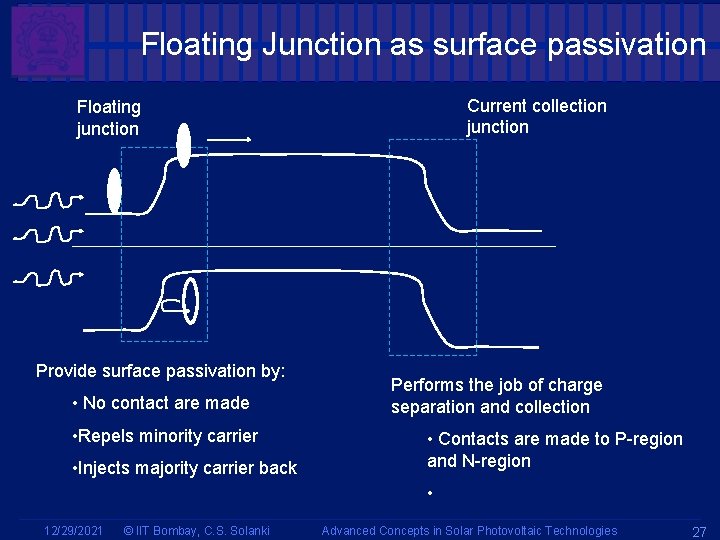
Floating Junction as surface passivation Current collection junction Floating junction Provide surface passivation by: • No contact are made • Repels minority carrier • Injects majority carrier back Performs the job of charge separation and collection • Contacts are made to P-region and N-region • 12/29/2021 © IIT Bombay, C. S. Solanki Advanced Concepts in Solar Photovoltaic Technologies 27
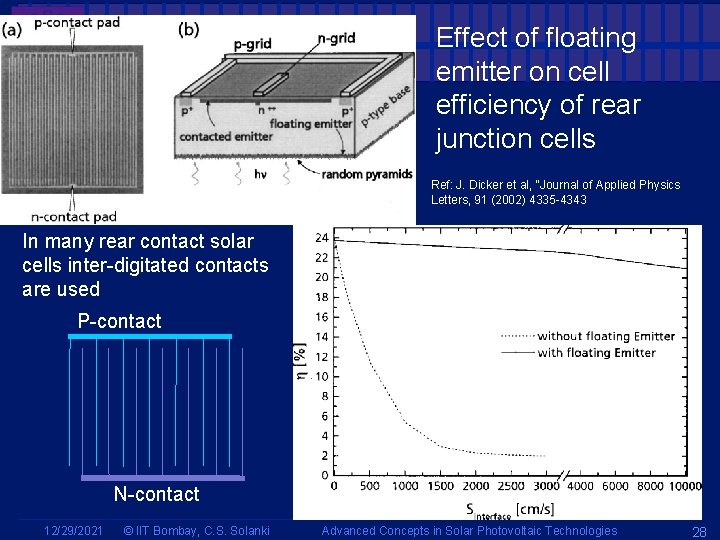
Effect of floating emitter on cell efficiency of rear junction cells Ref: J. Dicker et al, “Journal of Applied Physics Letters, 91 (2002) 4335 -4343 In many rear contact solar cells inter-digitated contacts are used P-contact N-contact 12/29/2021 © IIT Bombay, C. S. Solanki Advanced Concepts in Solar Photovoltaic Technologies 28
Back surface passivation of rear junction cells q. Back contacted solar cell has both junction at back side q. Choice of material and process parameter important for passivation layer q If passivation layer is based on field passivation, there should not be lateral path for current flow between base and emitter q preferably the rear passivation should be chemical based Si. O 2 passivation is good choice 12/29/2021 © IIT Bombay, C. S. Solanki Advanced Concepts in Solar Photovoltaic Technologies 29
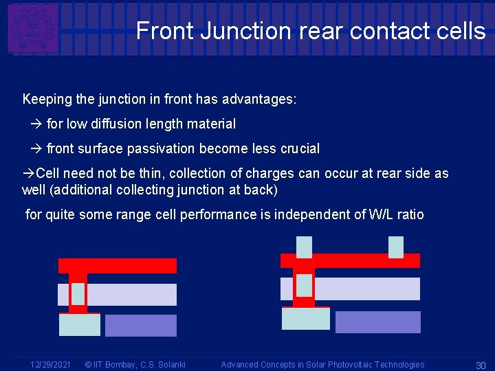
Front Junction rear contact cells Keeping the junction in front has advantages: for low diffusion length material front surface passivation become less crucial Cell need not be thin, collection of charges can occur at rear side as well (additional collecting junction at back) for quite some range cell performance is independent of W/L ratio 12/29/2021 © IIT Bombay, C. S. Solanki Advanced Concepts in Solar Photovoltaic Technologies 30
EWT and MWT EWT: The via or hole are made by photolithography and etching or more commonly by application of laser Hole densities above 100 cm-2 (about 1 mm apart) are needed to keep the resistive losses sufficiently low (otherwise an issue) A typical via spacing of 1 mm would require almost 25 000 holes in a 156 cm 2 substrate takes time. MWT Simpler than EWT Finger contact is on front only the use of bus bar and interconnection of cells is brought to rear contact Connection can be brought either via or externally, Resistance is not an issue, industrial processes can be used 12/29/2021 © IIT Bombay, C. S. Solanki Advanced Concepts in Solar Photovoltaic Technologies 31
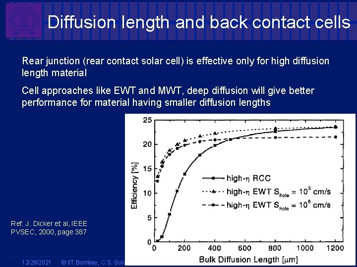
Diffusion length and back contact cells Rear junction (rear contact solar cell) is effective only for high diffusion length material Cell approaches like EWT and MWT, deep diffusion will give better performance for material having smaller diffusion lengths Ref: J. Dicker et al, IEEE PVSEC, 2000, page 387 12/29/2021 © IIT Bombay, C. S. Solanki Advanced Concepts in Solar Photovoltaic Technologies 32
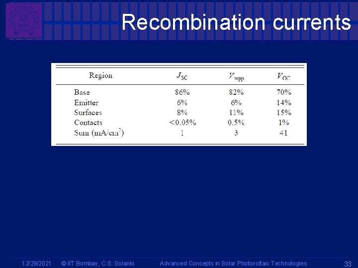
Recombination currents 12/29/2021 © IIT Bombay, C. S. Solanki Advanced Concepts in Solar Photovoltaic Technologies 33
Metal-Wrap-Through solar cell Ref: Tobias Fellmeth et al, Solar Energy Materials & Solar Cells 94 (2010) 1996– 2001 Thanks Som Mondal for compiling it
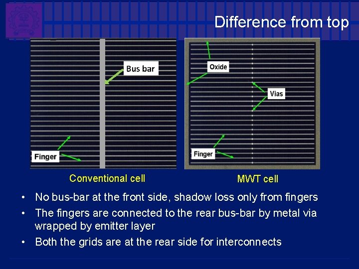
Difference from top Conventional cell MWT cell • No bus-bar at the front side, shadow loss only from fingers • The fingers are connected to the rear bus-bar by metal via wrapped by emitter layer • Both the grids are at the rear side for interconnects
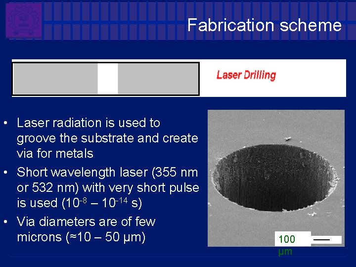
Fabrication scheme • Laser radiation is used to groove the substrate and create via for metals • Short wavelength laser (355 nm or 532 nm) with very short pulse is used (10 -8 – 10 -14 s) • Via diameters are of few microns (≈10 – 50 µm) 100 µm
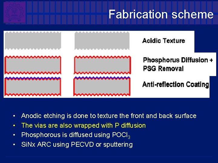
Fabrication scheme • • Anodic etching is done to texture the front and back surface The vias are also wrapped with P diffusion Phosphorous is diffused using POCl 3 Si. Nx ARC using PECVD or sputtering
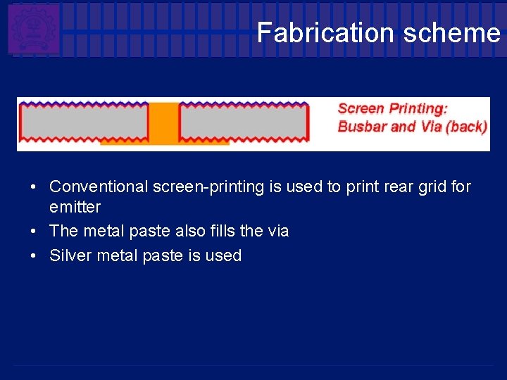
Fabrication scheme • Conventional screen-printing is used to print rear grid for emitter • The metal paste also fills the via • Silver metal paste is used
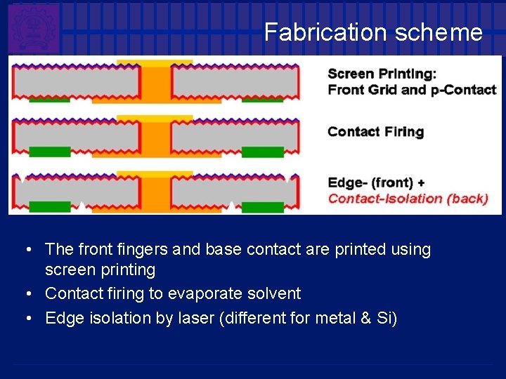
Fabrication scheme • The front fingers and base contact are printed using screen printing • Contact firing to evaporate solvent • Edge isolation by laser (different for metal & Si)
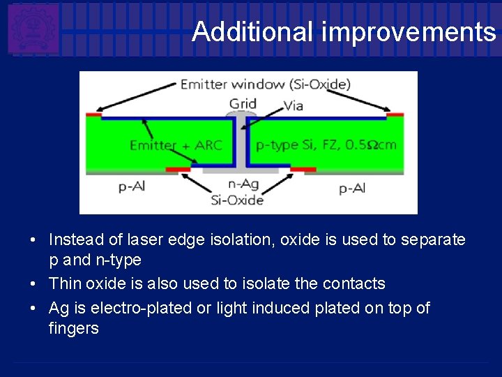
Additional improvements • Instead of laser edge isolation, oxide is used to separate p and n-type • Thin oxide is also used to isolate the contacts • Ag is electro-plated or light induced plated on top of fingers
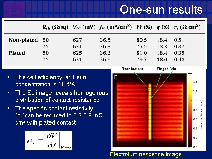
One-sun results • The cell efficiency at 1 sun concentration is 18. 6% • The EL image reveals homogenous distribution of contact resistance • The specific contact resistivity (ρc)can be reduced to 0. 8 -0. 9 mΩcm 2 with plated contact Electroluminescence image
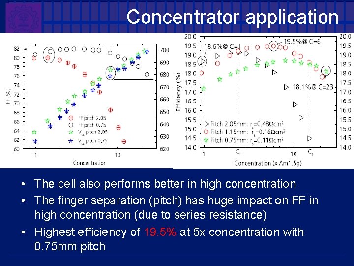
Concentrator application • The cell also performs better in high concentration • The finger separation (pitch) has huge impact on FF in high concentration (due to series resistance) • Highest efficiency of 19. 5% at 5 x concentration with 0. 75 mm pitch
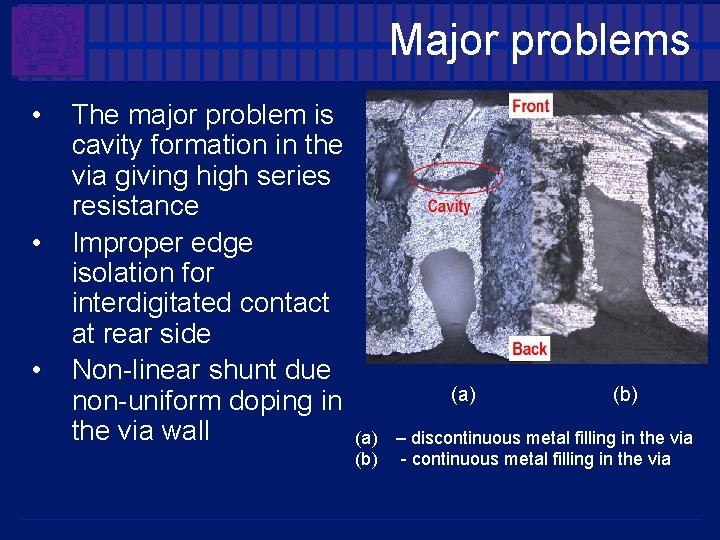
Major problems • • • The major problem is cavity formation in the via giving high series resistance Improper edge isolation for interdigitated contact at rear side Non-linear shunt due non-uniform doping in the via wall (a) (b) (a) – discontinuous metal filling in the via (b) - continuous metal filling in the via
- Slides: 43