High Current Impact Ionization Model 18 th HICUM

![Electric field at high current density Electric Field 10 5 [V/m] 0 0. 8 Electric field at high current density Electric Field 10 5 [V/m] 0 0. 8](https://slidetodoc.com/presentation_image_h/0250fec598ee1d082573213dd391a98a/image-9.jpg)
- Slides: 18

High Current Impact Ionization Model 18 th HICUM Workshop 2018 Munich, 19 June 2018 Mathieu Jaoul (ST, U. of Bordeaux), Cristell Maneux, T. Zimmer (U. of Bordeaux) and Didier Céli (ST)

Outline • Purpose • Evolution of the electric field at high current density • Impact Ionization field dependent model • Comparison of HICUM with ST HBTs measurement • Conclusion 2

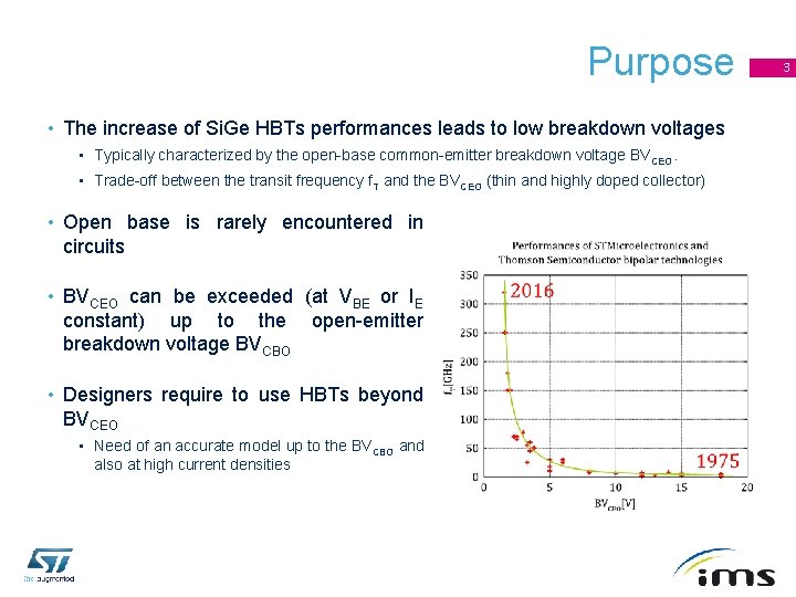
Purpose • The increase of Si. Ge HBTs performances leads to low breakdown voltages • Typically characterized by the open-base common-emitter breakdown voltage BVCEO. • Trade-off between the transit frequency f. T and the BVCEO (thin and highly doped collector) • Open base is rarely encountered in circuits • BVCEO can be exceeded (at VBE or IE constant) up to the open-emitter breakdown voltage BVCBO • Designers require to use HBTs beyond BVCEO • Need of an accurate model up to the BVCBO and also at high current densities 3

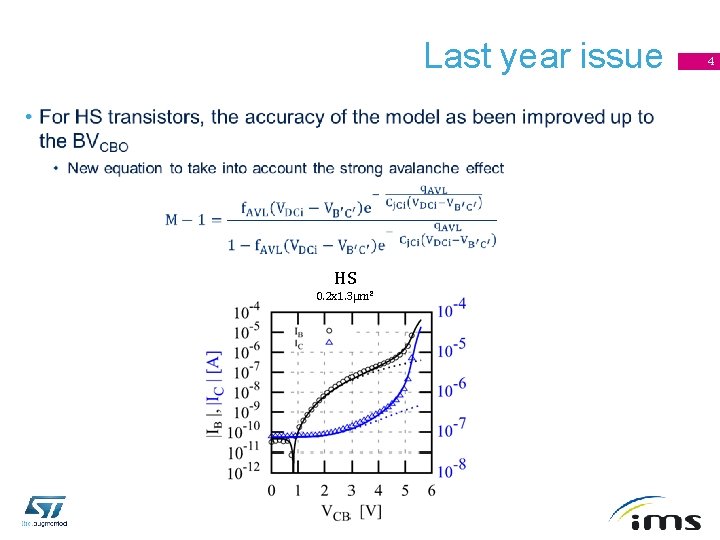
Last year issue • HS 0. 2 x 1. 3µm² 4

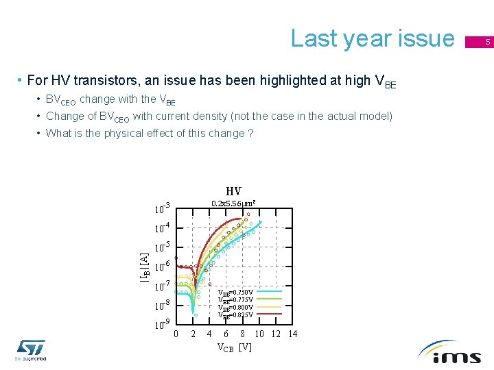
Last year issue • For HV transistors, an issue has been highlighted at high VBE • BVCEO change with the VBE • Change of BVCEO with current density (not the case in the actual model) • What is the physical effect of this change ? HV 0. 2 x 5. 56µm² -3 10 -4 10 10 | -6 | IB [A] -5 10 10 -7 VBE=0. 750 V VBE=0. 775 V VBE=0. 800 V VBE=0. 825 V -8 10 -9 10 0 2 4 6 8 10 12 14 VCB [V] 5

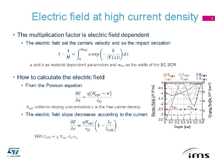
Electric field at high current density 6 10 -5 IC@f. T 0. 5 IC@f. T 2 IC@f. T Electric Field 105 [V/m] 0 0. 8 IC@f. T 3. 5 IC@f. T 8 -0. 5 6 -1 -1. 5 -2 -2. 5 4 w. BC w. Ch 2 -3 -3. 5 0 0 0. 1 0. 2 0. 3 0. 4 0. 5 0. 6 Depth [um] Doping Profile 1017 [cm-3] •

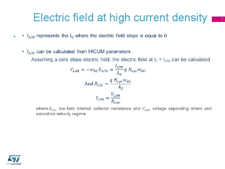
Electric field at high current density • 7

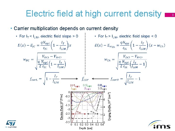
Electric field at high current density • Carrier multiplication depends on current density 10 -5 IC@f. T 0. 5 IC@f. T 2 IC@f. T Electric Field 105 [V/m] 0 0. 8 IC@f. T 3. 5 IC@f. T 8 -0. 5 6 -1 -1. 5 4 -2 w. BC -2. 5 w. Ch 2 -3 -3. 5 0 0 0. 1 0. 2 0. 3 0. 4 0. 5 0. 6 Depth [um] Doping Profile 1017 [cm-3] 8
![Electric field at high current density Electric Field 10 5 Vm 0 0 8 Electric field at high current density Electric Field 10 5 [V/m] 0 0. 8](https://slidetodoc.com/presentation_image_h/0250fec598ee1d082573213dd391a98a/image-9.jpg)
Electric field at high current density Electric Field 10 5 [V/m] 0 0. 8 IC@f. T 3. 5 IC@f. T 8 -0. 5 6 -1 -1. 5 4 -2 w. BC -2. 5 w. Ch 2 -3 -3. 5 0 0 0. 1 0. 2 0. 3 0. 4 0. 5 0. 6 Depth [um] 10 -5 IC@f. T 0 0. 12 IC@f. T 3 IC@f. T 0. 5 IC@f. T 4 IC@f. T 8 -0. 5 6 -1 -1. 5 4 -2 -2. 5 2 xhor -3 -3. 5 0 0 0. 1 0. 2 0. 3 0. 4 0. 5 0. 6 Depth [um] Doping Profile 1017 [cm-3] 0. 5 IC@f. T 2 IC@f. T Electric Field 10 5 [V/m] 10 -5 IC@f. T Doping Profile 1017 [cm-3] • 9

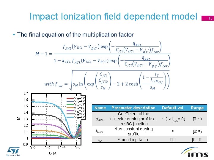
Impact Ionization field dependent model • 1. 7 VCB=3 V VCB=4 V VCB=5 V VCB=6 V VCB=7 V VCB=8 V VCB=9 V 1. 6 1. 5 M 1. 4 1. 3 1. 2 1. 1 1 0. 9 10 -6 10 -5 10 -4 IC [A] 10 -3 Name Parameter description Default val. Coefficient of the collector doping profile at ∞ (1/d. AVL= 0) the BC junction Non constant doping ∞ profile Smoothing factor 0. 1 Range [0: ∞) [0: 10] 10

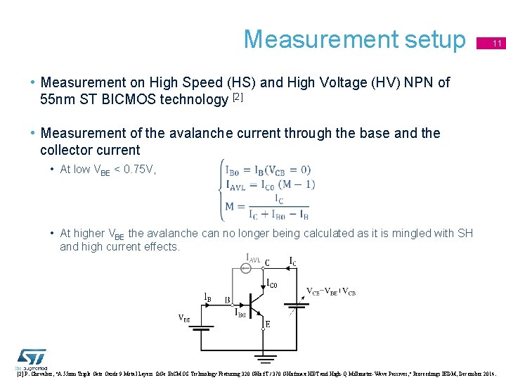
Measurement setup 11 • Measurement on High Speed (HS) and High Voltage (HV) NPN of 55 nm ST BICMOS technology [2] • Measurement of the avalanche current through the base and the collector current • At low VBE < 0. 75 V, • At higher VBE the avalanche can no longer being calculated as it is mingled with SH and high current effects. [2] P. Chevalier, "A 55 nm Triple Gate Oxide 9 Metal Layers Si. Ge Bi. CMOS Technology Featuring 320 GHz f. T / 370 GHz fmax HBT and High-Q Millimeter-Wave Passives, " Proceedings IEDM, December 2014.

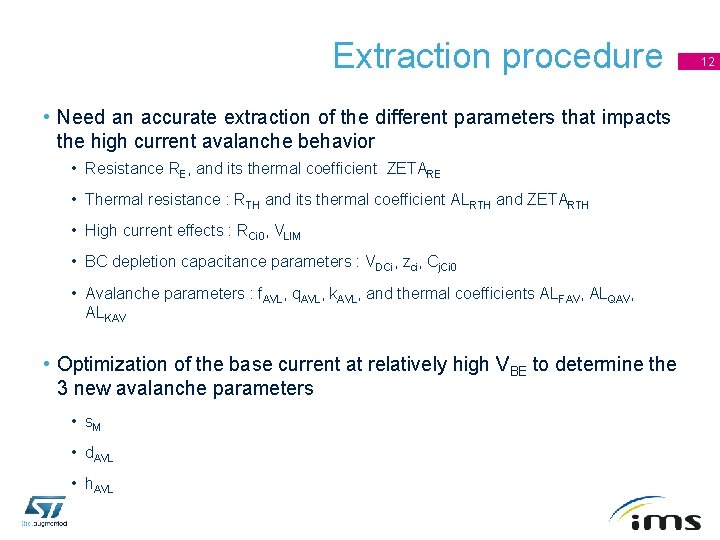
Extraction procedure • Need an accurate extraction of the different parameters that impacts the high current avalanche behavior • Resistance RE, and its thermal coefficient ZETARE • Thermal resistance : RTH and its thermal coefficient ALRTH and ZETARTH • High current effects : RCi 0, VLIM • BC depletion capacitance parameters : VDCi, zci, Cj. Ci 0 • Avalanche parameters : f. AVL, q. AVL, k. AVL, and thermal coefficients ALFAV, ALQAV, ALKAV • Optimization of the base current at relatively high VBE to determine the 3 new avalanche parameters • s. M • d. AVL • h. AVL 12

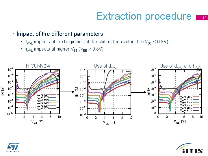
Extraction procedure 13 • Impact of the different parameters • d. AVL impacts at the beginning of the shift of the avalanche (VBE ≤ 0. 8 V) • h. AVL impacts at higher VBE (VBE ≥ 0. 8 V) HICUMv 2. 4 10 -3 Use of d. AVL 10 -4 10 -5 10 -6 10 -7 10 -8 -9 10 -8 10 -9 10 VBE =0. 700 V VBE =0. 725 V VBE =0. 750 V VBE =0. 775 V VBE =0. 800 V VBE =0. 825 V 0 2 4 6 VCE [V] 10 -7 10 -10 8 10 |IB | [A] -4 10 -7 10 -10 0 2 4 6 VCE [V] Use of d. AVL and h. AVL 10 -3 10 |IB | [A] 10 -3 8 10 10 VBE=0. 700 V VBE=0. 725 V VBE=0. 750 V VBE=0. 775 V VBE=0. 800 V VBE=0. 825 V -10 0 2 4 6 VCE [V] 8 10

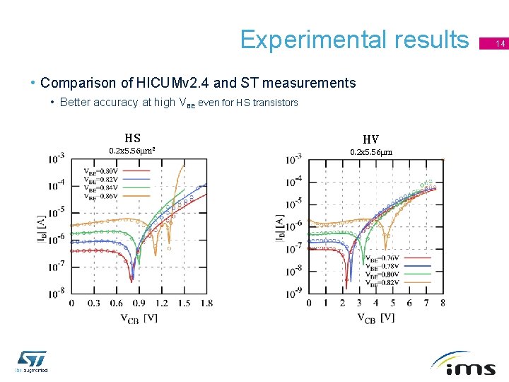
Experimental results • Comparison of HICUMv 2. 4 and ST measurements • Better accuracy at high VBE even for HS transistors HS HV 0. 2 x 5. 56µm² 0. 2 x 5. 56µm 14

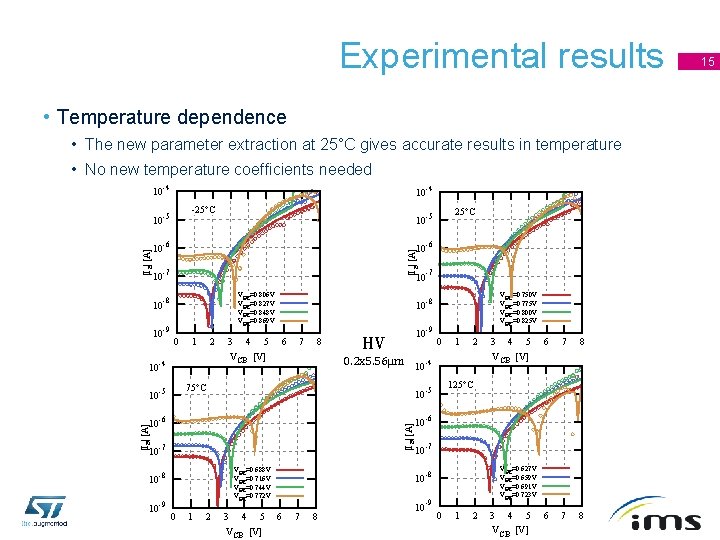
Experimental results • Temperature dependence • The new parameter extraction at 25°C gives accurate results in temperature • No new temperature coefficients needed 10 -5 10 -6 10 -7 10 -8 10 -9 10 10 -25°C VBE=0. 806 V VBE=0. 827 V VBE=0. 848 V VBE=0. 869 V 0 2 -4 -6 10 -7 10 -8 10 -9 10 -6 10 -7 10 -8 10 -9 6 7 8 HV 1 2 VBE=0. 750 V VBE=0. 775 V VBE=0. 800 V VBE=0. 825 V 0 3 4 5 VCB [V] 1 2 10 -6 10 -7 10 -8 6 7 8 10 -9 3 4 5 VCB [V] 6 7 8 125°C 10 -5 VBE=0. 688 V VBE=0. 716 V VBE=0. 744 V VBE=0. 772 V 0 25°C 0. 2 x 5. 56µm 10 -4 |I B| [A] 10 3 4 5 VCB [V] 75°C 10 -5 |I B| [A] 1 -4 10 -5 |I B| [A] -4 |I B| [A] 10 VBE=0. 627 V VBE=0. 659 V VBE=0. 691 V VBE=0. 723 V 0 1 2 3 4 5 VCB [V] 15

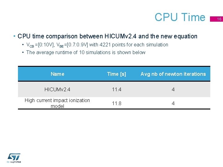
CPU Time • CPU time comparison between HICUMv 2. 4 and the new equation • VCB =[0: 10 V], VBE=[0. 7: 0. 9 V] with 4221 points for each simulation • The average runtime of 10 simulations is shown below Name Time [s] Avg nb of newton iterations HICUMv 2. 4 11. 4 4 High current impact ionization model 11. 8 4 16

Conclusion • Because of the reduction of the usable operating area a model that is accurate at high electric field (high VCB) and for currents close to the f. T peak is required • The accuracy of the model has been improved • In particular, for relatively low doped collector (HV transistors) • The model has been validated for a wide range of • VBE • VCB • Temperatures • Geometries • Devices • No convergence issues or drastic increase of the runtime has been 17

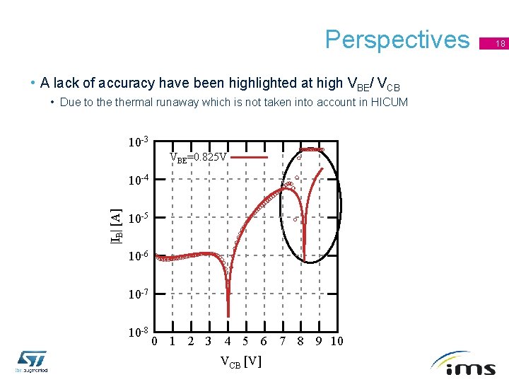
Perspectives • A lack of accuracy have been highlighted at high VBE/ VCB • Due to thermal runaway which is not taken into account in HICUM 10 -3 VBE=0. 825 V |IB| [A] 10 -4 10 -5 10 -6 10 -7 10 -8 0 1 2 3 4 5 6 7 8 9 10 VCB [V] 18