HFT PIXEL DAQ Prototype Testing Leo Greiner IPHC

- Slides: 18

HFT PIXEL DAQ Prototype Testing Leo Greiner IPHC meeting 2008 -04 -03 1

Outline • • • Review of RDO design. Motivation for system test LVDS Single Ladder Data Path test design Status and Conclusions Application to Phase-1 and Ultimate For more information, please see: http: //rnc. lbl. gov/hft/hardware/docs/LVDS/index. html Leo Greiner IPHC meeting 2008 -04 -03 2

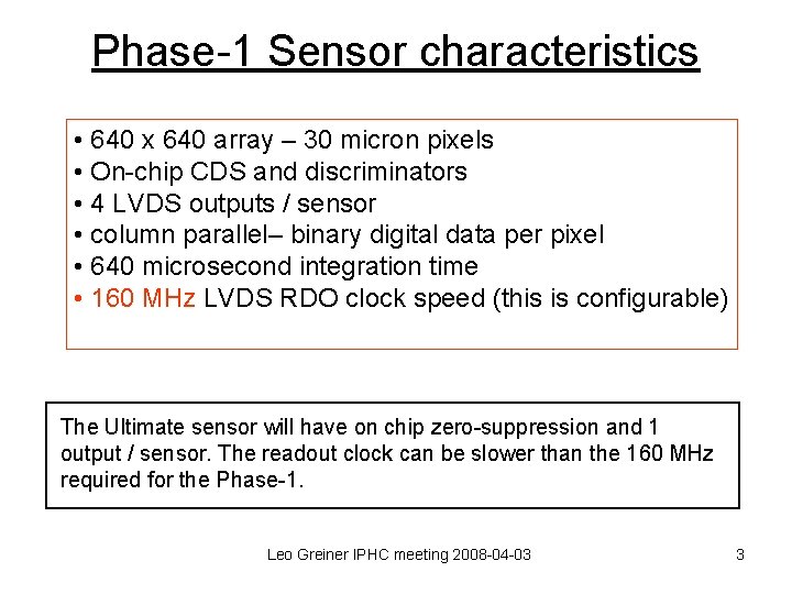
Phase-1 Sensor characteristics • 640 x 640 array – 30 micron pixels • On-chip CDS and discriminators • 4 LVDS outputs / sensor • column parallel– binary digital data per pixel • 640 microsecond integration time • 160 MHz LVDS RDO clock speed (this is configurable) The Ultimate sensor will have on chip zero-suppression and 1 output / sensor. The readout clock can be slower than the 160 MHz required for the Phase-1. Leo Greiner IPHC meeting 2008 -04 -03 3

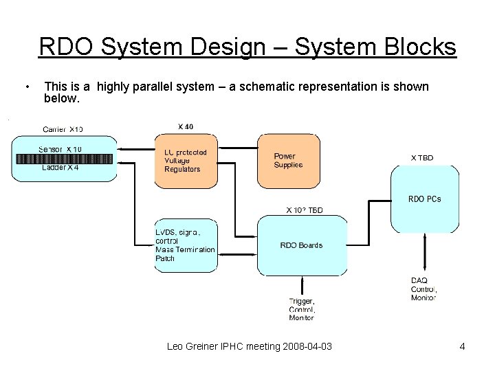
RDO System Design – System Blocks • This is a highly parallel system – a schematic representation is shown below. Leo Greiner IPHC meeting 2008 -04 -03 4

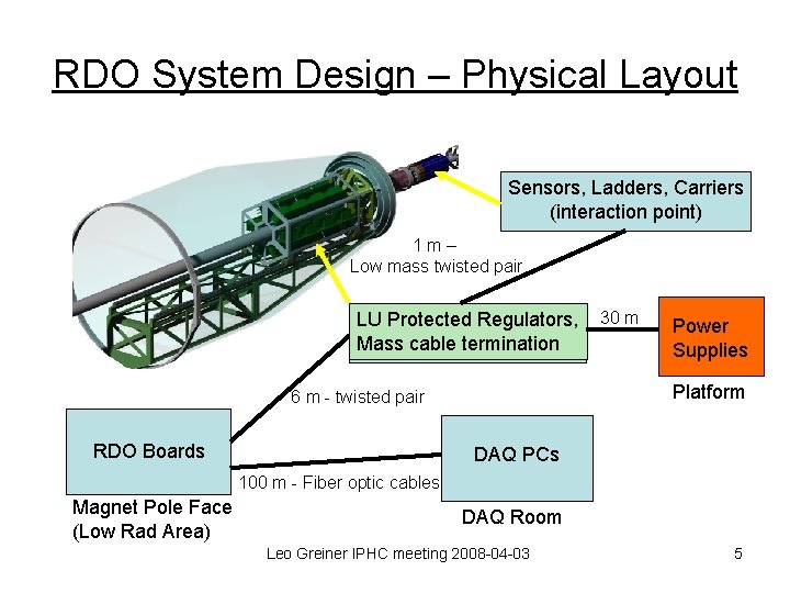
RDO System Design – Physical Layout Sensors, Ladders, Carriers (interaction point) 1 m– Low mass twisted pair LU Protected Regulators, Mass cable termination Power Supplies Platform 6 m - twisted pair RDO Boards 30 m DAQ PCs 100 m - Fiber optic cables Magnet Pole Face (Low Rad Area) DAQ Room Leo Greiner IPHC meeting 2008 -04 -03 5

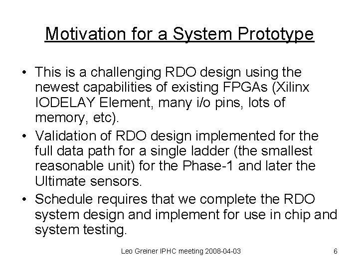
Motivation for a System Prototype • This is a challenging RDO design using the newest capabilities of existing FPGAs (Xilinx IODELAY Element, many i/o pins, lots of memory, etc). • Validation of RDO design implemented for the full data path for a single ladder (the smallest reasonable unit) for the Phase-1 and later the Ultimate sensors. • Schedule requires that we complete the RDO system design and implement for use in chip and system testing. Leo Greiner IPHC meeting 2008 -04 -03 6

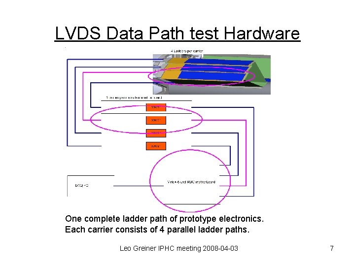
LVDS Data Path test Hardware One complete ladder path of prototype electronics. Each carrier consists of 4 parallel ladder paths. Leo Greiner IPHC meeting 2008 -04 -03 7

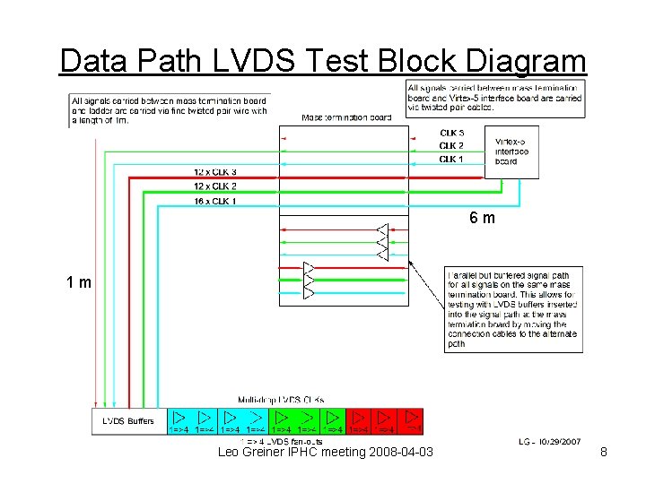
Data Path LVDS Test Block Diagram 6 m 1 m Leo Greiner IPHC meeting 2008 -04 -03 8

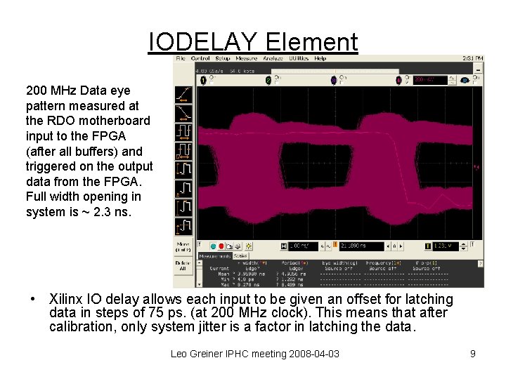
IODELAY Element 200 MHz Data eye pattern measured at the RDO motherboard input to the FPGA (after all buffers) and triggered on the output data from the FPGA. Full width opening in system is ~ 2. 3 ns. • Xilinx IO delay allows each input to be given an offset for latching data in steps of 75 ps. (at 200 MHz clock). This means that after calibration, only system jitter is a factor in latching the data. Leo Greiner IPHC meeting 2008 -04 -03 9

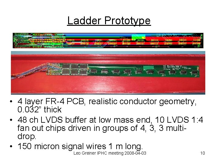
Ladder Prototype • 4 layer FR-4 PCB, realistic conductor geometry, 0. 032” thick • 48 ch LVDS buffer at low mass end, 10 LVDS 1: 4 fan out chips driven in groups of 4, 3, 3 multidrop. • 150 micron signal wires 1 m long. Leo Greiner IPHC meeting 2008 -04 -03 10

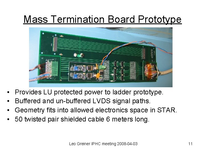
Mass Termination Board Prototype • • Provides LU protected power to ladder prototype. Buffered and un-buffered LVDS signal paths. Geometry fits into allowed electronics space in STAR. 50 twisted pair shielded cable 6 meters long. Leo Greiner IPHC meeting 2008 -04 -03 11

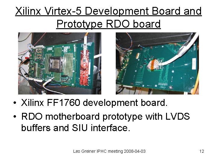
Xilinx Virtex-5 Development Board and Prototype RDO board • Xilinx FF 1760 development board. • RDO motherboard prototype with LVDS buffers and SIU interface. Leo Greiner IPHC meeting 2008 -04 -03 12

What is tested? • 1 full data path for a complete ladder. • Multi-drop in groups on 4, 3, 3. • Cross-talk through the whole system – each muti -drop group carries different random data. • The signal paths on the PCBs and the cabling are as comparable as possible to the final implementation. • External SIU communication software/firmware to set IODELAY for each channel. • Bit error rate for different read out frequencies, paths, cables, etc. Leo Greiner IPHC meeting 2008 -04 -03 13

Status • All boards are in hand, the system is assembled and testing has begun. • Initial runs looked very good – 12 hr @ 200 MHz with no bit errors. • Currently we are seeing bit errors at a very low rate 1 in 1011 to 1013 at all frequencies from 160 to 240 MHz. • Troubleshooting is underway but this will involve development of new firmware and software specifically designed for error detection and trapping at a low rate and may take some time. Leo Greiner IPHC meeting 2008 -04 -03 14

Conclusions • We have prototyped a one ladder RDO data path in a detector system that consists of 40 parallel ladder readout systems. • Initial tests look good. We currently have a very small bit error rate that is under investigation. • The prototyping is considered a success as the existing error rate is quite acceptable and would result in a very small inefficiency or fake hit rate in the Phase-1 detector. (Ultimate can be read out more slowly) We fully expect to fix the whatever is causing the errors that we do see. • The RDO system architecture is considered to be validated and we will now work on the design of the full functionality prototypes for the RDO system. Leo Greiner IPHC meeting 2008 -04 -03 15

Implications for Phase-1 and Ultimate designs • Does Phase-1 require a 50% duty cycle clock? The realities of running the clock from the FPGA through cables and buffers leave a clock with a duty cycle less than 50%. • Doing the IODELAY calculation requires a set of capabilities built into the test patterns that can be received from the Phase-1 and Ultimate Sensors. These are enumerated in a document written by Chinh Vu given on the next page… Leo Greiner IPHC meeting 2008 -04 -03 16

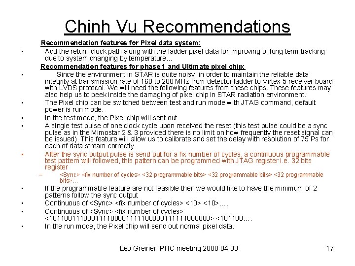
Chinh Vu Recommendations • • • Recommendation features for Pixel data system: Add the return clock path along with the ladder pixel data for improving of long term tracking due to system changing by temperature… Recommendation features for phase 1 and Ultimate pixel chip: Since the environment in STAR is quite noisy, in order to maintain the reliable data integrity at transmission rate of 160 to 200 MHz from detector ladder to Virtex 5 -receiver board with LVDS protocol. We will need the following features from these chips. These features may also help us to peek inside the damaging of pixel chip in STAR radiation environment. The Pixel chip can be switched between test and run mode with JTAG command, default power is run mode. In the test mode, the Pixel chip will sent out A single test pulse of one clock cycle upon received the reset (this test pulse could be a sync pulse as in the Mimostar 2 & 3 provided there is no limit on how frequently the reset signal can be issued). This feature will allow us to calibrate and set the delay with resolution of 75 Ps for each of data stream correctly. After the sync output pulse is send out for a fix number of cycles, a continuous programmable test pattern will followed, this pattern can be programmed with JTAG register i. e. 32 bits register – • • <Sync> <fix number of cycles> <32 programmable bits>… If the programmable feature are not feasible then we would like to have the minimum of 2 patterns follow the sync output Continuous of <Sync> <fix number of cycles> <10>…. Continuous of <Sync> <fix number of cycles> <101100111000111100001111100000111111000000> <101100…. In the run mode, the Pixel chip will send out normal pixel data. Leo Greiner IPHC meeting 2008 -04 -03 17

fin Leo Greiner IPHC meeting 2008 -04 -03 18