HEMTs in Europe Ga As HEMT lownoise technologies

- Slides: 35

HEMTs in Europe (Ga. As HEMT low-noise technologies, design techniques, characterization and modeling) Ernesto Limiti E. E. Dept. head, University of Rome “Tor Vergata”, Rome, Italy limiti@ing. uniroma 2. it E. E. Dept. University of Roma Tor Vergata, Roma, Italy Improving the future now

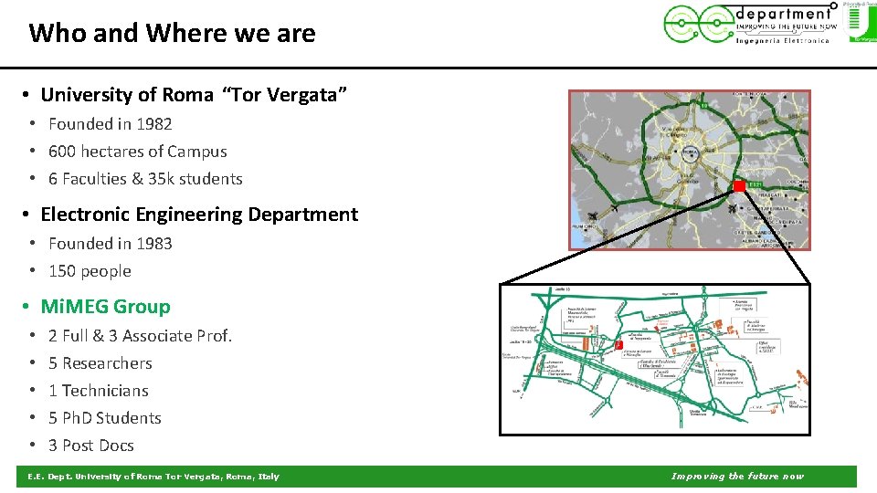
Who and Where we are • University of Roma “Tor Vergata” • Founded in 1982 • 600 hectares of Campus • 6 Faculties & 35 k students • Electronic Engineering Department • Founded in 1983 • 150 people • Mi. MEG Group • • • 2 Full & 3 Associate Prof. 5 Researchers 1 Technicians 5 Ph. D Students 3 Post Docs E. E. Dept. University of Roma Tor Vergata, Roma, Italy Improving the future now

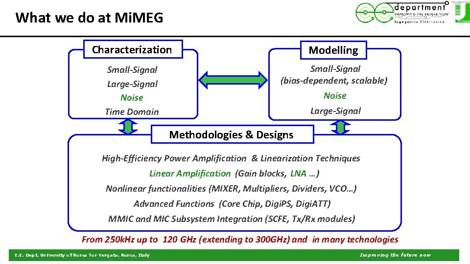
What we do at Mi. MEG Characterization Modelling Small-Signal Large-Signal Noise Time Domain Small-Signal (bias-dependent, scalable) Noise Large-Signal Methodologies & Designs High-Efficiency Power Amplification & Linearization Techniques Linear Amplification (Gain blocks, LNA …) Nonlinear functionalities (MIXER, Multipliers, Dividers, VCO…) Advanced Functions (Core Chip, Digi. PS, Digi. ATT) MMIC and MIC Subsystem Integration (SCFE, Tx/Rx modules) From 250 k. Hz up to 120 GHz (extending to 300 GHz) and in many technologies E. E. Dept. University of Roma Tor Vergata, Roma, Italy Improving the future now

Low-Noise Ga. As HEMT technologies in Europe E. E. Dept. University of Roma Tor Vergata, Roma, Italy Improving the future now

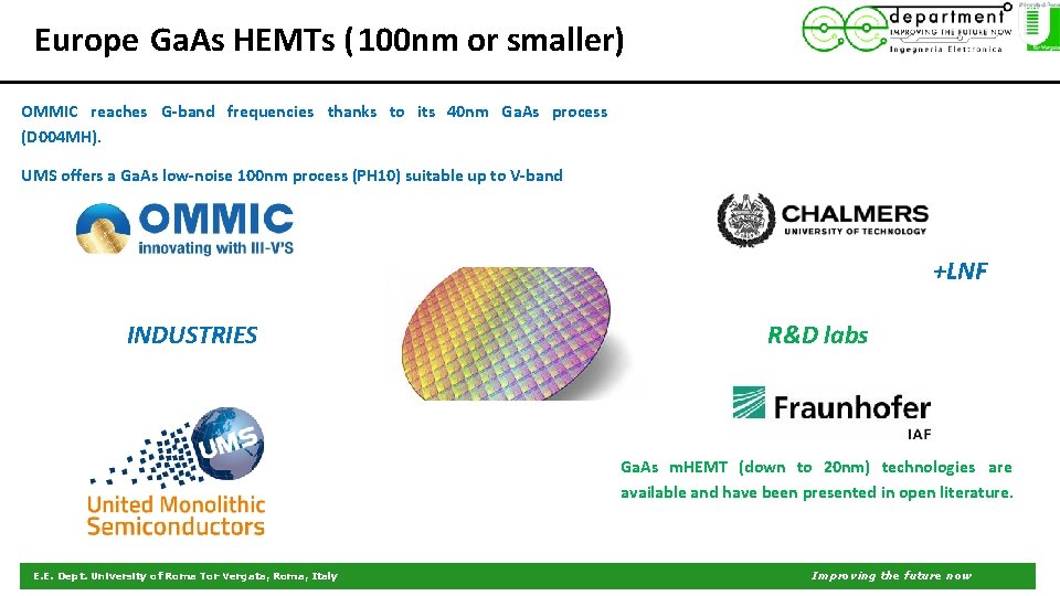
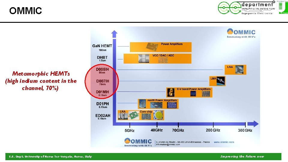
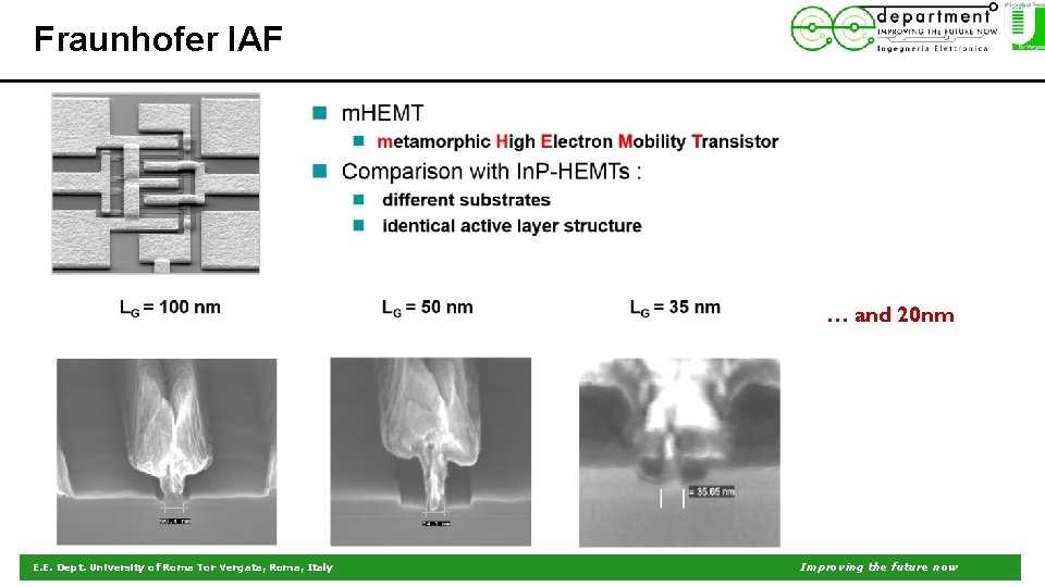
Europe Ga. As HEMTs (100 nm or smaller) OMMIC reaches G-band frequencies thanks to its 40 nm Ga. As process (D 004 MH). UMS offers a Ga. As low-noise 100 nm process (PH 10) suitable up to V-band +LNF INDUSTRIES R&D labs Ga. As m. HEMT (down to 20 nm) technologies are available and have been presented in open literature. E. E. Dept. University of Roma Tor Vergata, Roma, Italy Improving the future now

OMMIC Metamorphic HEMTs (high indium content in the channel, 70%) E. E. Dept. University of Roma Tor Vergata, Roma, Italy Improving the future now

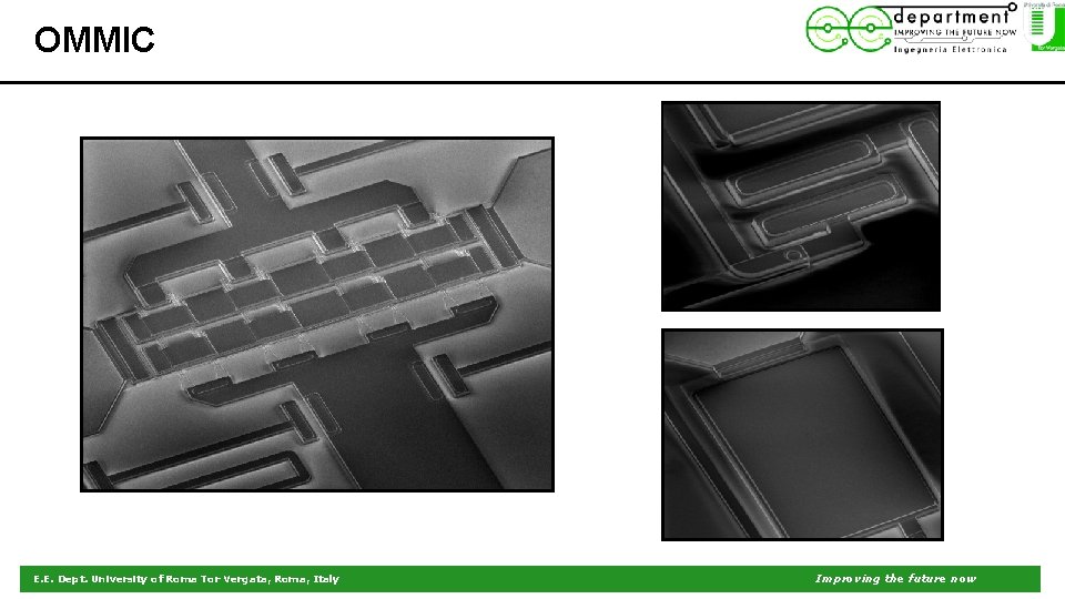
OMMIC E. E. Dept. University of Roma Tor Vergata, Roma, Italy Improving the future now

Fraunhofer IAF … and 20 nm E. E. Dept. University of Roma Tor Vergata, Roma, Italy Improving the future now

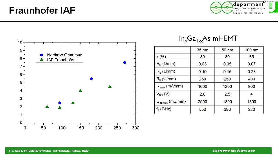
Fraunhofer IAF Inx. Ga 1 -x. As m. HEMT E. E. Dept. University of Roma Tor Vergata, Roma, Italy Improving the future now

Low-Noise Design Techniques E. E. Dept. University of Roma Tor Vergata, Roma, Italy Improving the future now

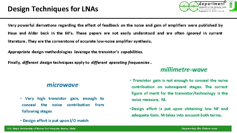
Design Techniques for LNAs Very powerful derivations regarding the effect of feedback on the noise and gain of amplifiers were published by Haus and Alder back in the 60’s. These papers are not easily understood and are often ignored in current literature. They are the cornerstone of accurate low-noise amplifier synthesis. Appropriate design methodologies leverage the transistor’s capabilities. Finally, different design techniques apply to different operating frequencies. microwave • Very high transistor gain, enough to conceal the noise contribution from following stages • Design effort is put upon I/O match E. E. Dept. University of Roma Tor Vergata, Roma, Italy millimetre-wave • Transistor gain is not enough to conceal the noise contribution on subsequent stages. The correct figure of merit for the transistor/technology is the noise measure, M. • Design effort is put upon obtaining low NF and adequate Gain. M takes into account both terms. Improving the future now

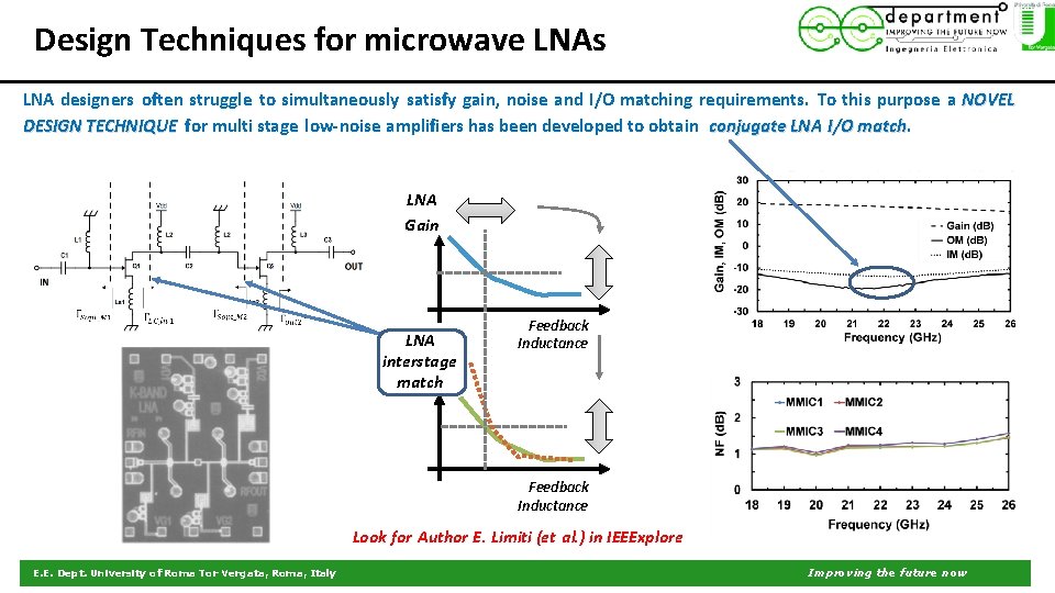
Design Techniques for microwave LNAs LNA designers often struggle to simultaneously satisfy gain, noise and I/O matching requirements. To this purpose a NOVEL DESIGN TECHNIQUE for multi stage low-noise amplifiers has been developed to obtain conjugate LNA I/O match LNA Gain LNA interstage match Feedback Inductance Look for Author E. Limiti (et al. ) in IEEExplore E. E. Dept. University of Roma Tor Vergata, Roma, Italy Improving the future now

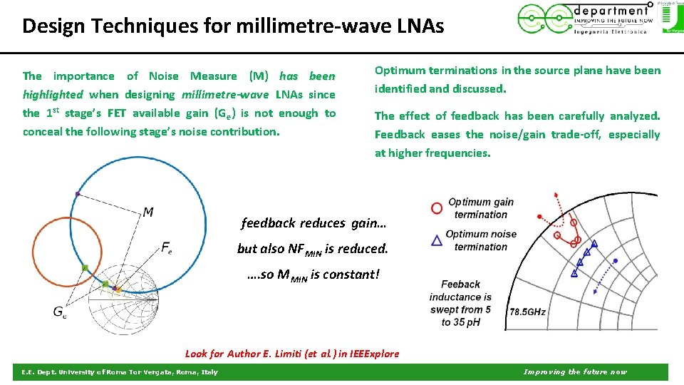
Design Techniques for millimetre-wave LNAs The importance of Noise Measure (M) has been highlighted when designing millimetre-wave LNAs since the 1 st stage’s FET available gain (Ge) is not enough to conceal the following stage’s noise contribution. Optimum terminations in the source plane have been identified and discussed. The effect of feedback has been carefully analyzed. Feedback eases the noise/gain trade-off, especially at higher frequencies. feedback reduces gain… but also NF MIN is reduced. …. so M MIN is constant! Look for Author E. Limiti (et al. ) in IEEExplore E. E. Dept. University of Roma Tor Vergata, Roma, Italy Improving the future now

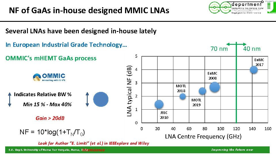
NF of Ga. As in-house designed MMIC LNAs Several LNAs have been designed in-house lately In European Industrial Grade Technology… 70 nm 40 nm OMMIC’s m. HEMT Ga. As process Eu. MC 2017 Eu. MC 2008 MOTL 2018 Indicates Relative BW % MOTL 2019 Min 15 % - Max 40% Gain > 20 d. B JSSC 2010 NF = 10*log(1+TN/T 0) Look for Author “E. Limiti” (et al. ) in IEEExplore and Wiley E. E. Dept. University of Roma Tor Vergata, Roma, Italy Interscience Improving the future now

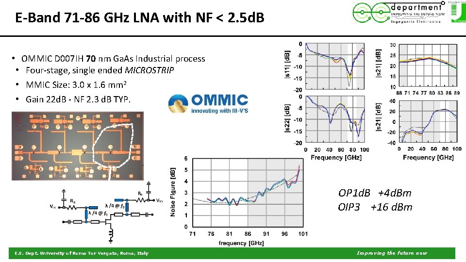
E-Band 71 -86 GHz LNA with NF < 2. 5 d. B • OMMIC D 007 IH 70 nm Ga. As Industrial process • Four-stage, single ended MICROSTRIP • MMIC Size: 3. 0 x 1. 6 mm 2 • Gain 22 d. B - NF 2. 3 d. B TYP. OP 1 d. B +4 d. Bm OIP 3 +16 d. Bm E. E. Dept. University of Roma Tor Vergata, Roma, Italy Improving the future now

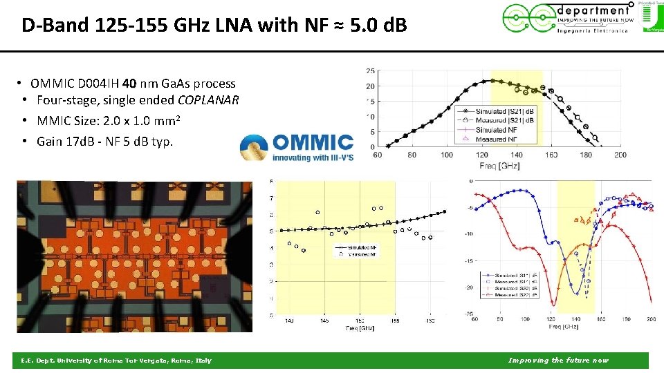
D-Band 125 -155 GHz LNA with NF ≈ 5. 0 d. B • OMMIC D 004 IH 40 nm Ga. As process • Four-stage, single ended COPLANAR • MMIC Size: 2. 0 x 1. 0 mm 2 • Gain 17 d. B - NF 5 d. B typ. E. E. Dept. University of Roma Tor Vergata, Roma, Italy Improving the future now

Low-Noise Analysis, characterization and modelling capabilities E. E. Dept. University of Roma Tor Vergata, Roma, Italy Improving the future now

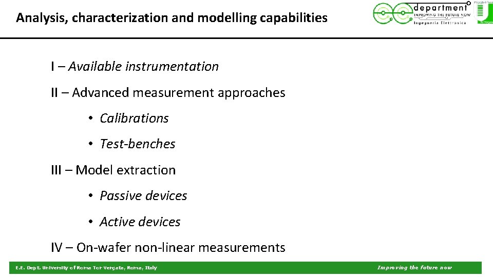
Analysis, characterization and modelling capabilities I – Available instrumentation II – Advanced measurement approaches • Calibrations • Test-benches III – Model extraction • Passive devices • Active devices IV – On-wafer non-linear measurements E. E. Dept. University of Roma Tor Vergata, Roma, Italy Improving the future now

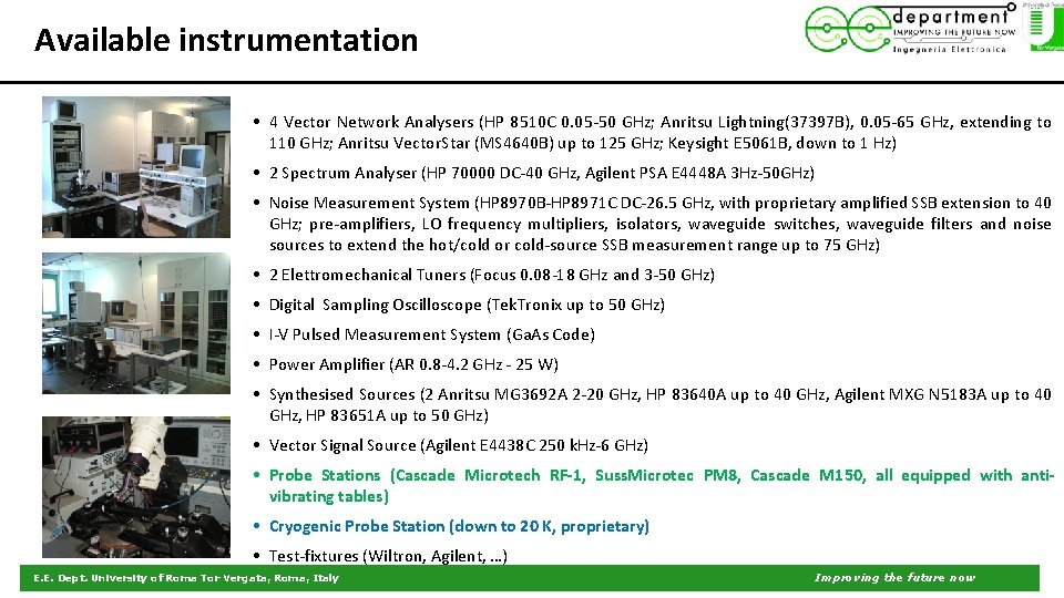
Available instrumentation • 4 Vector Network Analysers (HP 8510 C 0. 05 -50 GHz; Anritsu Lightning(37397 B), 0. 05 -65 GHz, extending to 110 GHz; Anritsu Vector. Star (MS 4640 B) up to 125 GHz; Keysight E 5061 B, down to 1 Hz) • 2 Spectrum Analyser (HP 70000 DC-40 GHz, Agilent PSA E 4448 A 3 Hz-50 GHz) • Noise Measurement System (HP 8970 B-HP 8971 C DC-26. 5 GHz, with proprietary amplified SSB extension to 40 GHz; pre-amplifiers, LO frequency multipliers, isolators, waveguide switches, waveguide filters and noise sources to extend the hot/cold or cold-source SSB measurement range up to 75 GHz) • 2 Elettromechanical Tuners (Focus 0. 08 -18 GHz and 3 -50 GHz) • Digital Sampling Oscilloscope (Tek. Tronix up to 50 GHz) • I-V Pulsed Measurement System (Ga. As Code) • Power Amplifier (AR 0. 8 -4. 2 GHz - 25 W) • Synthesised Sources (2 Anritsu MG 3692 A 2 -20 GHz, HP 83640 A up to 40 GHz, Agilent MXG N 5183 A up to 40 GHz, HP 83651 A up to 50 GHz) • Vector Signal Source (Agilent E 4438 C 250 k. Hz-6 GHz) • Probe Stations (Cascade Microtech RF-1, Suss. Microtec PM 8, Cascade M 150, all equipped with antivibrating tables) • Cryogenic Probe Station (down to 20 K, proprietary) • Test-fixtures (Wiltron, Agilent, …) E. E. Dept. University of Roma Tor Vergata, Roma, Italy Improving the future now

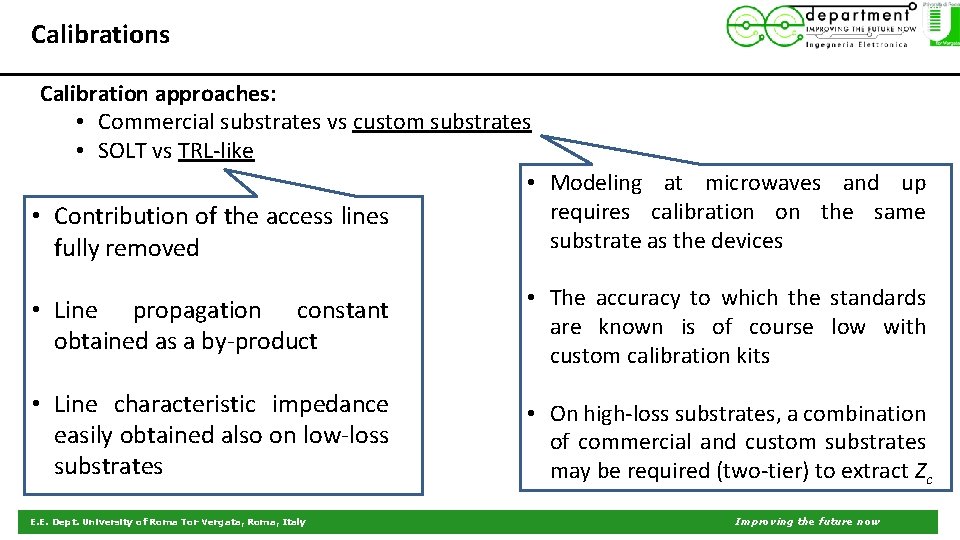
Calibrations Calibration approaches: • Commercial substrates vs custom substrates • SOLT vs TRL-like • Modeling at microwaves and up requires calibration on the same • Contribution of the access lines substrate as the devices fully removed • Line propagation constant obtained as a by-product • The accuracy to which the standards are known is of course low with custom calibration kits • Line characteristic impedance easily obtained also on low-loss substrates • On high-loss substrates, a combination of commercial and custom substrates may be required (two-tier) to extract Zc E. E. Dept. University of Roma Tor Vergata, Roma, Italy Improving the future now

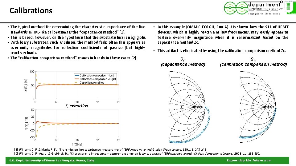
Calibrations • The typical method for determining the characteristic impedance of the line standards in TRL-like calibrations is the “capacitance method” [1]. • This is based, however, on the hypothesis that the substrate loss is negligible. • With lossy substrates, such as Silicon, the method fails: often this appears as over-unity magnitudes for reflection coefficients of passive (but highly reactive) loads. • The “calibration comparison method” comes in handy in these cases [2]. • In this example (OMMIC D 01 GH, Run A) it is shown how the S 11 of HEMT devices, which is highly reactive at low frequencies, may easily appear to feature over-unity magnitude when it is renormalized based on the capacitance method Zc. • This artifact is eliminated by using the calibration comparison method Zc S 11 (capacitance method) S 11 (calibration comparison method) Zc extraction [1] Williams D. F. & Marks R. B. , “Transmission line capacitance measurement. ” IEEE Microwave and Guided Wave Letters, 1991, 1, 243 -245 [2] Williams D. F. , Arz U. & Grabinski H. , “Characteristic-impedance measurement error on lossy substrates. ” IEEE Microwave and Wireless Components Letters, 2001, 11, 299 -301 E. E. Dept. University of Roma Tor Vergata, Roma, Italy . Improving the future now

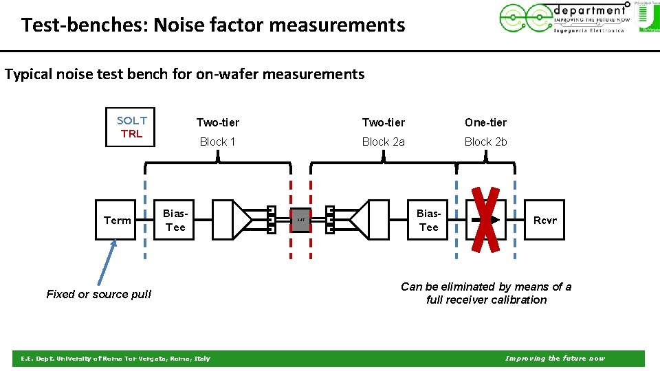
Test-benches: Noise factor measurements Typical noise test bench for on-wafer measurements SOLT TRL Term Two-tier One-tier Block 1 Block 2 a Block 2 b Bias. Tee Fixed or source pull E. E. Dept. University of Roma Tor Vergata, Roma, Italy DUT Bias. Tee Rcvr Can be eliminated by means of a full receiver calibration Improving the future now

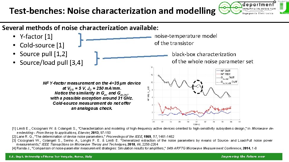
Test-benches: Noise characterization and modelling Several methods of noise characterization available: noise-temperature model • Y-factor [1] of the transistor • Cold-source [1] black-box characterization • Source pull [1, 2] of the whole noise parameter set • Source/load pull [3, 4] NF Y-factor measurement on the 4× 35 µm device at VDS = 5 V, JD = 250 m. A/mm. Notice the similarity in Gav and Gav, hc, with a possible exception around 31 GHz. Cold-source measurement do not offer an analogous check. [1] Limiti E. , Ciccognani W. & Colangeli S. , “Characterization and modeling of high-frequency active devices oriented to high-sensitivity subsystems design, ” in Microwave deembedding - From theory to applications, Elsevier, 2013, 97 -150 [2] Lane R. Q. , “The determination of device noise parameters, ” Proceedings of the IEEE, 1969, 57, 1461 -1462 [3] Ciccognani W. , Colangeli S. , Serino A. , Longhi P. E. & Limiti E. “Generalized extraction of the noise parameters by means of Source- and Load-Pull noise power measurements, ” IEEE Transactions on Microwave Theory and Techniques, 2018, 66, 2258 -2264 [4] Randa J. , “Comparison of noise-parameter measurement strategies: Simulation results for amplifiers, ” 84 th ARFTG Microwave Measurement Conference, 2014, 1 -8 E. E. Dept. University of Roma Tor Vergata, Roma, Italy Improving the future now

Test-benches: Source/load pull Better conditioned system of equations resulting in reduced uncertainty in the estimation of F min and Rn. E. E. Dept. University of Roma Tor Vergata, Roma, Italy Improving the future now

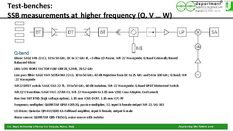
Test-benches: SSB measurements at higher frequency (Q, V … W) Q-band Mixer: SAGE SFB-22 -E 2, 33 to 50 GHz, DC to 17 GHz IF, +3 d. Bm LO Power, WR-22 Waveguide, Q Band Externally Biased Balanced Mixer LNA: LOW NOISE FACTORY LNF-LNR 28_52 WB, 28 -52 GHz Low pass filter: SAGE SWF-50354340 -22 -L 1, 30 to 50 GHz, 40 d. B Rejection from DC to 25 GHz and 56 to 100 GHz, Q Band, WR -22 Waveguide WR 22 DPDT switch: SAGE SWJ-22 -TS, 33 to 50 GHz, 60 d. B Isolation, WR-22 Waveguide, Q Band DPDT Motorized Switch WR 22/V transition: SAGE SWC-22 VM-E 1, WR-22 Waveguide to 1. 85 mm V(M) Coax Adapter, End Launch Bias tee: SHF BT 65 (high voltage option), 1. 85 mm V(M)-DCRF, 1. 85 mm V(F)-RF Frequency multiplier: QUINSTAR QPM-42052 Q, passive multiplier, X 2, input k-female output WR-22, UG-383 LO driver: Quinstar QPI-K 0238 JO KA-Fullband amplifier, input k-female, output k-male Noise source: QUINSTAR QNS-FB 15 LQ, noise source with isolator E. E. Dept. University of Roma Tor Vergata, Roma, Italy Improving the future now

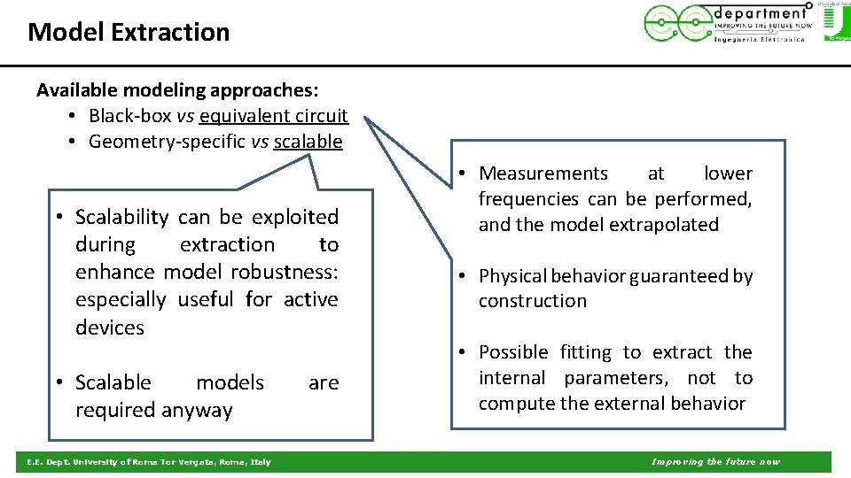
Model Extraction Available modeling approaches: • Black-box vs equivalent circuit • Geometry-specific vs scalable • Scalability can be exploited during extraction to enhance model robustness: especially useful for active devices • Scalable models required anyway E. E. Dept. University of Roma Tor Vergata, Roma, Italy are • Measurements at lower frequencies can be performed, and the model extrapolated • Physical behavior guaranteed by construction • Possible fitting to extract the internal parameters, not to compute the external behavior Improving the future now

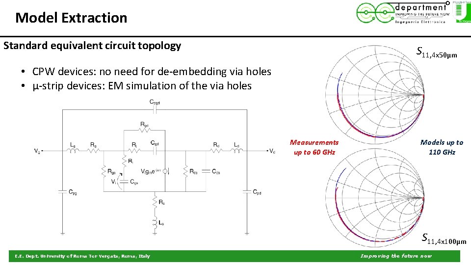
Model Extraction Standard equivalent circuit topology S 11, 4 x 50μm • CPW devices: no need for de-embedding via holes • μ-strip devices: EM simulation of the via holes Measurements up to 60 GHz Models up to 110 GHz S 11, 4 x 100μm E. E. Dept. University of Roma Tor Vergata, Roma, Italy Improving the future now

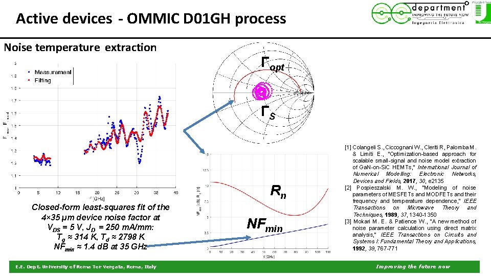
Active devices - OMMIC D 01 GH process Noise temperature extraction Γopt ΓS Rn Closed-form least-squares fit of the 4× 35 µm device noise factor at VDS = 5 V, JD = 250 m. A/mm: Tg ≈ 314 K, Td ≈ 2798 K NFmin ≈ 1. 4 d. B at 35 GHz E. E. Dept. University of Roma Tor Vergata, Roma, Italy NFmin [1] Colangeli S. , Ciccognani W. , Cleriti R, Palomba M. & Limiti E. , “Optimization-based approach for scalable small-signal and noise model extraction of Ga. N-on-Si. C HEMTs, ” International Journal of Numerical Modelling: Electronic Networks, Devices and Fields, 2017, 30, e 2135 [2] Pospieszalski M. W. , “Modeling of noise parameters of MESFETs and MODFETs and their frequency and temperature dependence, ” IEEE Transactions on Microwave Theory and Techniques, 1989, 37, 1340 -1350 [3] Mokari M. E. & Patience W. , “A new method of noise parameter calculation using direct matrix analysis, ” IEEE Transactions on Circuits and Systems I: Fundamental Theory and Applications, 1992, 39, 767 -771 Improving the future now

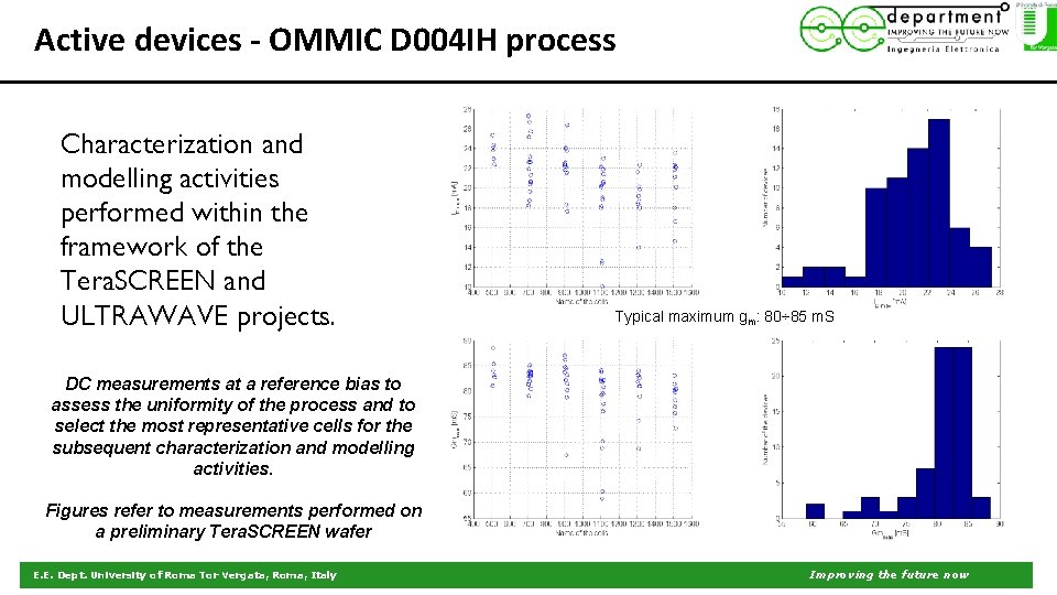
Active devices - OMMIC D 004 IH process Characterization and modelling activities performed within the framework of the Tera. SCREEN and ULTRAWAVE projects. Typical maximum gm: 80÷ 85 m. S DC measurements at a reference bias to assess the uniformity of the process and to select the most representative cells for the subsequent characterization and modelling activities. Figures refer to measurements performed on a preliminary Tera. SCREEN wafer E. E. Dept. University of Roma Tor Vergata, Roma, Italy Improving the future now

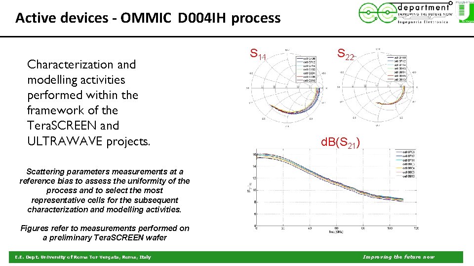
Active devices - OMMIC D 004 IH process Characterization and modelling activities performed within the framework of the Tera. SCREEN and ULTRAWAVE projects. S 11 S 22 d. B(S 21) Scattering parameters measurements at a reference bias to assess the uniformity of the process and to select the most representative cells for the subsequent characterization and modelling activities. Figures refer to measurements performed on a preliminary Tera. SCREEN wafer E. E. Dept. University of Roma Tor Vergata, Roma, Italy Improving the future now

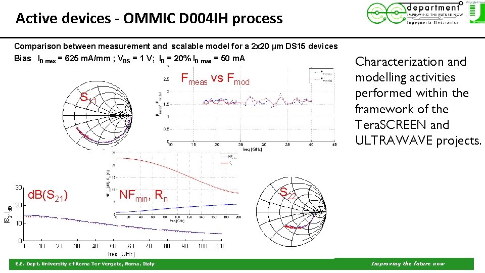
Active devices - OMMIC D 004 IH process Comparison between measurement and scalable model for a 2 x 20 µm DS 15 devices Bias ID max = 625 m. A/mm ; VDS = 1 V; ID = 20% ID max = 50 m. A Fmeas vs Fmod S 11 d. B(S 21) NFmin, Rn E. E. Dept. University of Roma Tor Vergata, Roma, Italy Characterization and modelling activities performed within the framework of the Tera. SCREEN and ULTRAWAVE projects. S 22 Improving the future now

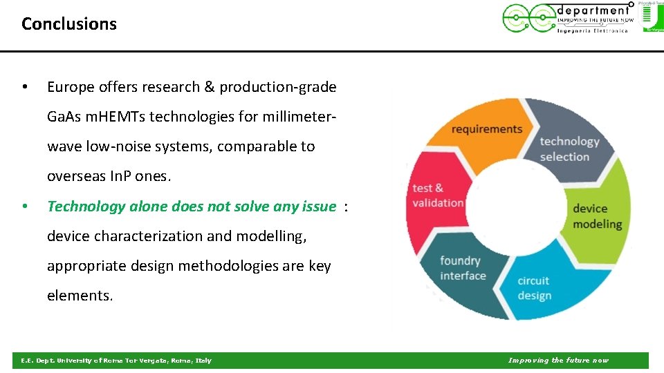
Conclusions • Europe offers research & production-grade Ga. As m. HEMTs technologies for millimeterwave low-noise systems, comparable to overseas In. P ones. • Technology alone does not solve any issue : device characterization and modelling, appropriate design methodologies are key elements. E. E. Dept. University of Roma Tor Vergata, Roma, Italy Improving the future now

HEMTs in Europe (Ga. As HEMT low-noise technologies, design techniques, characterization and modeling) Ernesto Limiti E. E. Dept. head, University of Rome “Tor Vergata”, Rome, Italy limiti@ing. uniroma 2. it E. E. Dept. University of Roma Tor Vergata, Roma, Italy Improving the future now

References • Low-Noise Amplifier Design Techniques 1. Ciccognani, W. , Longhi, P. E. , Colangeli, S. , Limiti, E. , “Constant mismatch circles and application to low-noise microwave amplifier design”, IEEE Transactions on Microwave Theory and Techniques, 61(12), 6662458, pp. 4154 -4167, 2013. 2. Ciccognani, W. , Colangeli, S. , Limiti, E. , Longhi, P. “Noise measure-based design methodology for simultaneously matched multi-stage lownoise amplifiers”, IET Circuits, Devices and Systems, 6(1), pp. 63 -70, 2012. 3. Colangeli, S. , Ciccognani, W. , Salvucci, A. , Limiti, E. , “Deterministic design of simultaneously matched, two-stage low-noise amplifiers”, Asia. Pacific Microwave Conference Proceedings, pp. 558 -561, 2018. • Low-Noise Active Devices Characterization & Modeling 1. Ciccognani, W. , Colangeli, S. , Serino, A. , Longhi, P. E. , Limiti, E. , “Generalized Extraction of the Noise Parameters by Means of Source-and Load-Pull Noise Power Measurements” IEEE Transactions on Microwave Theory and Techniques, 66(5), pp. 2258 -2264, 2018. 2. Colangeli, S. , Ciccognani, W. , Palomba, M. , Limiti, E. , “Automated extraction of device noise parameters based on multi-frequency, source-pull data”, International Journal of Microwave and Wireless Technologies, 6(1), pp. 63 -72, 2014. 3. Cleriti, R. , Ciccognani, W. , Colangeli, S. , (. . . ), Frijlink, P. , Renvoisé, M. , “Characterization and modelling of 40 nm m. HEMT process up to 110 GHz”, 11 th European Microwave Integrated Circuits Conference, pp. 353 -356, 2016 4. Cleriti, R. , Colangeli, S. , Ciccognani, W. , Palomba, M. , Limiti, E. , “Cold-source cryogenic characterization and modeling of a m. HEMT process”, European Microwave Week, pp. 41 -44, 2015. E. E. Dept. University of Roma Tor Vergata, Roma, Italy Improving the future now

Reference • Millimetre-wave Ga. As LNAs 1. Ciccognani, W. , Colangeli, S. , Longhi, P. E. , Limiti, E. , “Design of a MMIC low-noise amplifier in industrial gallium arsenide technology for Eband 5 G transceivers”, Microwave and Optical Technology Letters 61(1), pp. 205 -210, 2019. 2. Ciccognani, W. , Longhi, P. E. , Colangeli, S. , Limiti, E. “Q/V band LNA for satellite on-board space applications using a 70 nanometers Ga. As m. HEMT commercial technology”, Microwave and Optical Technology Letters 60(9), pp. 2185 -2190, 2018. 3. Cleriti, R. , Ciccognani, W. , Colangeli, S. , et al. . , “D-band LNA using a 40 -nm Ga. As m. HEMT technology”, 12 th European Microwave Integrated Circuits Conference, pp. 105 -108, 2017. 4. Ciccognani, W. , Colangeli, S. , Limiti, E. , Scucchia, L. , “Millimeter wave low noise amplifier for satellite and radio-astronomy applications”, IEEE 1 st AESS European Conference on Satellite Telecommunications, ESTEL 2012. 5. Ciccognani, W. , Limiti, E. , Longhi, P. E. , Renvoisè, M. , “MMIC LNAs for radioastronomy applications using advanced industrial 70 nm metamorphic technology” IEEE Journal of Solid-State Circuits, 45(10), pp. 2008 -2015, 2010. 6. Ciccognani, W. , Giannini, F. , Limiti, E. , Longhi, P. E. , “Full W-band high-gain LNA in m. HEMT mmic technology” European Microwave Integrated Circuit Conference, Eu. MIC 2008, pp. 314 -317, 2008. E. E. Dept. University of Roma Tor Vergata, Roma, Italy Improving the future now