HEMT HIGH ELECTRON MOBILITY TRANSISTOR A BRIEF OVERVIEW

HEMT: HIGH ELECTRON MOBILITY TRANSISTOR A BRIEF OVERVIEW AND DESCRIPTION OF HEMT OPERATION, APPLICATIONS, STRUCTURE, AND MATERIALS. Andrew Ridderman 4/7/17

OUTLINE • Introduction • What are HEMT’s and how do they work? • • Materials and structure Characteristics and band diagram Versions of HEMT’s Applications • Summary and Conclusions • References • Key Concepts

INTRODUCTION • Invention of the HEMT is attributed to Takashi Mimura • HEMTs were first investigated in 1969 but were not implemented in a device until 1980 initially with a very high cost • Today the largest market for HEMT integrated circuits are wireless communications such as cellphones, WLAN, and CATV

WHAT ARE HEMT’S AND HOW DO THEY WORK? •

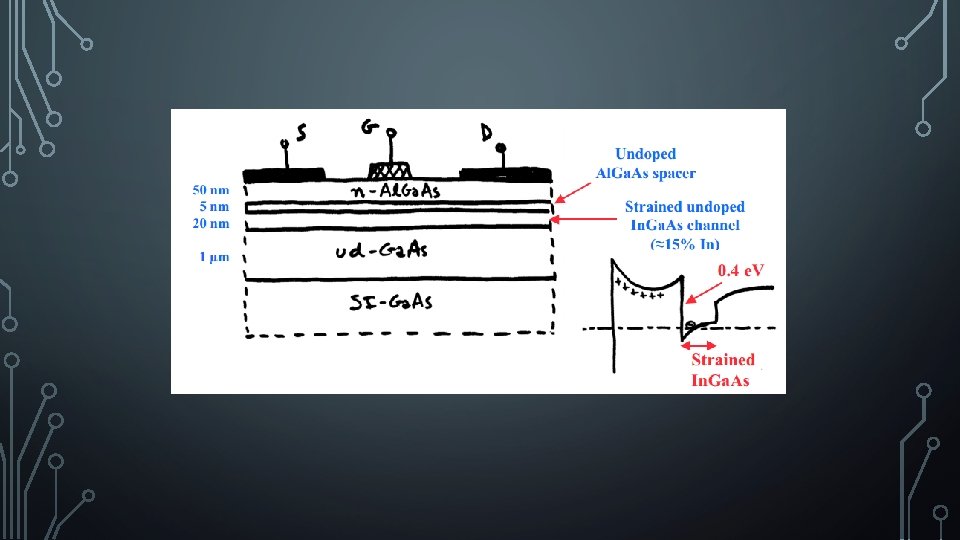
MATERIALS AND STRUCTURE • The most common materials used for HEMTs are Ga. As and Al. Ga. As • However In. P and Ga. N are also used in some cases for improved characteristics • The spacer layer seperates the 2 DEG from any ionized donors increasing mobility

CHARACTERISTICS AND BAND DIAGRAM • HEMT characteristics include high gain, high switching speed, low noise and very good high frequency performance • Cutoff frequencies of 100 GHz+ have been achieved • Higher mobility of HEMT also results in lower parasitic drain and source resistances • The biggest disadvantage of the HEMT is heterojunction fabrication is more complicated
 METAMORPHIC (MHEMT) • Uses an extremely thin layer of")
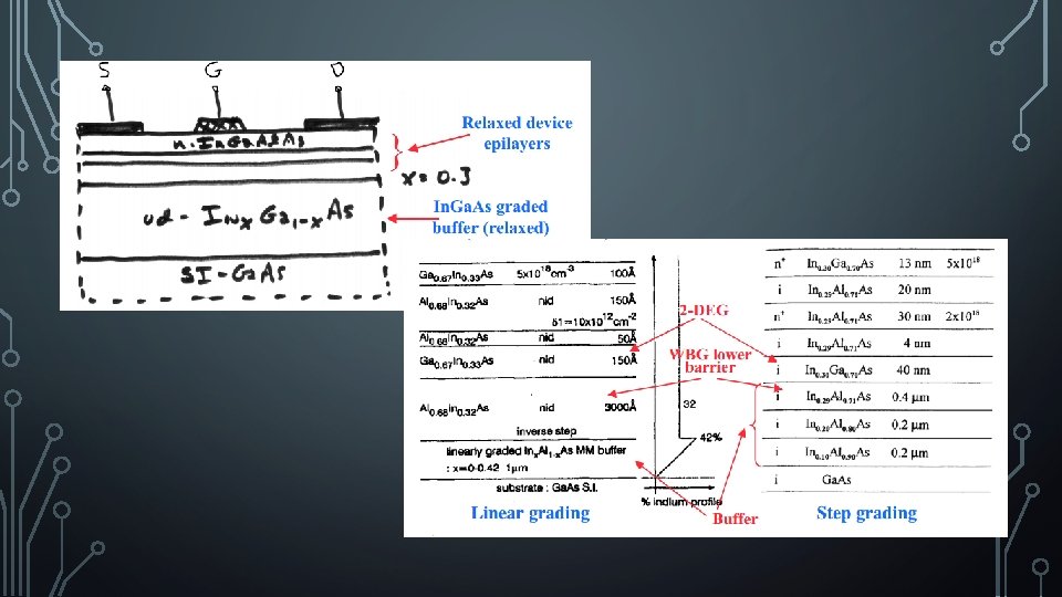
VERSIONS OF HEMT’S PSEUDOMORPHIC (PHEMT) METAMORPHIC (MHEMT) • Uses an extremely thin layer of one • Uses a buffer layer of to match the of the materials so that the crystal lattice stretches to fit the other material • Allows for larger bandgap differences resulting in better performance lattice of constant of both materials • Different Indium concentrations can be used to optimize the device for different applications

APPLICATIONS • Originally developed for high speed applications • Used in a wide range of RF applications including Microwave and millimeter wave communications, imaging, radar, and astronomy • Used in military and space applications such as electronic warfare systems and satellite communication • Applications where high frequencies, high gain and low noise are required • Ga. N HEMT is widely used in small signal amps, power amps, and oscillators because of its low on-state resistance and high switching speed

SUMMARY AND CONCLUSIONS HEMTs can operate a high frequency by utilizing the 2 DEG created by the hetrojunction which result in a very high electron mobility. The high frequencies and low noise achievable with HEMTs are great for high bandwidth RF communication applications. Different structure designs such as PHEMT and MHEMT further improve upon the standard HEMTs performance resulting in more desirable characteristics.

REFERENCES • http: //www. radio-electronics. com/info/data/semicond/fet-field-effect-transistor/hemt-phemttransistor. php • • • https: //parts. jpl. nasa. gov/mmic/3 -IV. PDF • • http: //www. iue. tuwien. ac. at/phd/brech/ch_6_2_2. htm • • http: //science 24. com/paper/12263 http: //www. ee. sc. edu/personal/faculty/simin/ELCT 871/18%20 Al. GAN-Ga. N%20 HEMTs. pdf https: //www. fujitsu. com/global/documents/about/resources/publications/fstj/archives/vol 501/paper 21. pdf http: //my. ece. ucsb. edu/Mishra/classfiles/overview. pdf http: //www. nrao. edu/meetings/isstt/papers/2009178182. pdf https: //ocw. mit. edu/courses/electrical-engineering-and-computer-science/6 -772 -compoundsemiconductor-devices-spring-2003/lecture-notes/Lecture 12 v 2. pdf http: //www-mtl. mit. edu/~alamo/pdf/2011/RC-189%20 slides. pdf

KEY CONCEPTS • 2 DEG has such a high mobility due to the channel layer having no dopant impurities • HEMT’s are mostly used in high performance applications where high frequency and low noise are needed • A heterojunction is a junction between materials with different band gaps • HEMT’s can be used in a large range of frequencies allowing for use in many different applications • The most used materials for HEMTs are Ga. As and Al. Ga. As
- Slides: 13