HDI Image Transfer Technology and Trend Charles Kao


 Definition • High Density Interconnect --- • 使用Mircovia 微孔技術的電路板 – 孔徑 6")


")


 • Process")


: – 重量 厚度 . – –")
 • Laminate Cu (T oz, 12")
 • Deposit electroless")
/2 –")


 Error • 曝光底片種類 • 底片漲縮參數 – 偶氮(Diazo 棕片) • Solder mask,")
 CHE (%)")


 • Varies with material")


 反射鏡 (Reflection Mirror) 冷鏡 (Dichroic Mirror) 曝光照射面 (Exposure Surface)")


 • TI 2004/4/15 72/80")


- Slides: 80
HDI Image Transfer Technology and Trend 志聖 業 高啟清博士 Charles Kao, Ph. D Tel: 02 -2601 -0700 Fax: 02 -2602 -1556 Mobile: 0939 -268 -725 cckao@csun. com. tw V 2. 1 2007/5/8
課程綱要 1. 2. 3. 4. 5. HDI Development 發展 HDI Structure 結構 HDI Major Process 製程 Fine Line Formation 技術課題 PCB影像移轉設備發展現況 2004/4/15 2/80
HDI Development From through to blind via
Methods to Increase PCB Density 1. Reduce hole and pad diameters – More space for routing – Increase cost, Process difficulty 2. Reduce conductor width – More channels between pads – Will increase cost, reduce board yield 3. Increase signal planes – More layers of PCBs – Increase cost 4. Use embedded passives – Increase surface area, reduce routing – Increase cost, Hadco/Sanmina patent issue 2004/4/15 4/80
HDI (Build-up) Definition • High Density Interconnect --- • 使用Mircovia 微孔技術的電路板 – 孔徑 6 mil (150 m) – IPC/JPCA-2315 Design Guide for HDI and Microvia • Purpose of HDI – More circuit, more via on smaller PCB • Design rule comparison HDI to MLB 2004/4/15 5/80
Electronic Assembly with HDI/Microvia 2004/4/15 6/80
Motorola Mobile phone Development • Lighter, Thinner, Shorter, Smaller 輕薄短小 • High frequency, High speed, Multi function 高頻, 高速, 多功能 2004/4/15 • Sequential lamination to form blind and buried via • Laser drill to form blind via • 2 layer laser vias 7/80
HDI Applications – Miniaturization – Camcorder L/S: 65/65~75/75 Via/Pad: 150/250 • Application – cellular phone, camcorder, notebook, PDA, GPS – 6~10 layer 1~2 buildup layers – Need PTH, IVH, BVH – Cellular phone L/S: 65/65~75/75 Via/Pad: 150/250 – Notebook PC L/S 75/75~100/100 Via/Pad: 125~200/250~400 Source: PCFab 1999/9, Tech. Search 2004/4/15 8/80
HDI Applications – IC Substrates • Package substrate • Microvia IC Substrate – Flip Chip, BGA, CSP, MCM, Hybrid – 6~12 layer, 1~3 buildup layers –需要IVH, BVH – 避免使用PTH, PTH IVH+BVH 2004/4/15 Source: PCFab 1999/9, Tech. Search – MPU L/S: 70/70 Via/Pad: 86/125 – ASIC Via/Pad: 75/150 9/80
HDI Application - High Layer Count • Application • Ibiden 1 -12 -1 – Router, Server, Base station, Workstation, Networking – 14~24, up to 32 layers, t=80~180 mil, up to 7. 6 mm – 1~2, up to 3 buildup layers – PTH, Aspect ratio 12: 1 – BVH, laser via – Low Dk=3. 4 – Low Df = 0. 005 – Impedance 8% 2004/4/15 10/80 • Ibiden 1 -20 -1
Embedded Passives • Embedded Resister • Buried Capacitor – Termination resistor – De-coupling, LC filter – Vcc - BC - GND – 在Power/Ground間 • Inductor – LC filter 2004/4/15 11/80
PCB Product Market Status • Micro via PCB and IC substrate will accounts 25% of market value in 2007 Source: Prismark, 2003 2004/4/15 12/80
PCB產品一般規格需求 PCB類別 線寬/線距 最小孔徑 環徑 對位精度 Card/Module 6~8 mil >150 m 0. 3 mm + 5 mil 2 mil/50 m Desktop PC 5/5 mil 125 m 0. 3 mm + 5 mil 2 mil/50 m Notebook板 4/4 mil 100 m 0. 25 mm + 3 mil 1. 2 mil/30 m HDI 手機板 3/3 mil 75 m 0. 25 mm 盲孔 150 m + 3 mil 1 mil/25 m BGA 載板 2/2 mil 50 m 0. 25 mm + 2 mil 0. 8 mil/20 m Flip chip 載板 1/1 mil 25 m 盲孔 75 m + 1 mil 0. 4 mil/10 m 2004/4/15 13/80
HDI Roadmap - Ibiden Source: www. ibiden. co. jp 2004/4/15 14/80
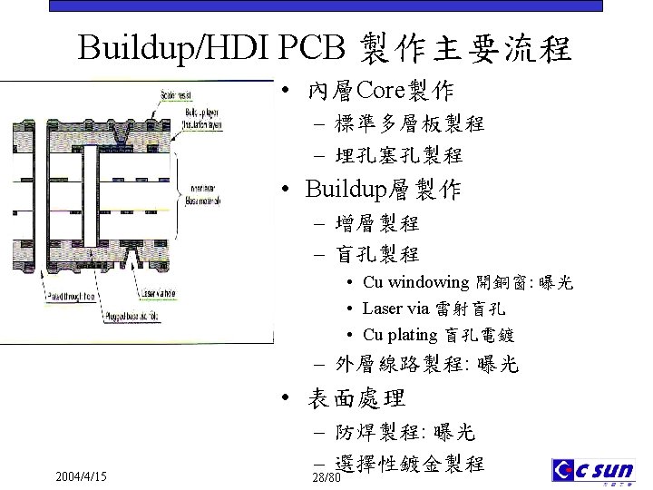
HDI PCB結構 (Buildup/HDI PCB)
多層板結構 線寬 Conductor Width 外層線路 線距 Conductor Space 孔環 Annular Ring 孔徑 內層 1 Inner Layer #1 內層 2 Inner Layer #2 內層線路 盲孔 Blind Via 絕緣介質層 Dielectric 2004/4/15 通孔 Through Hole 埋孔 Buried Via 增層法多層板 Build-up PCB 傳統多層板 Multi Layer PCB 16/80
Buildup PCB Structure • Buildup PCB 結構 • 導通孔型式演進 – 芯層 Core – 絕緣層 Buildup Dielectric – 盲埋孔 Blind / Buried Via • Buildup PCB表示法 – Face Buildup 層數 + Core 層數 + Back Buildup 層數 – 例: 1+4+1, 2+2+2, 2+4+2 2004/4/15 17/80 – Multi-layer PTH通孔 – Sequential lamination blind/buried via – 1 Layer blind via – 2 Layer blind via • Staggered Via • Skipped Via • Stacked Via – Via on PTH – Via in Via
Multi-layer Blind Via Configuration * Stacked Via 3 Level * Staggered Via * Skipped Via L 1 -L 3 2004/4/15 18/80 * Stacked Via L 1 -L 2 -L 3
Advanced Microvia Configuration • Via on PTH – 塞孔不能凹陷 – 注意Peeling Strength不足 • Via in via • Cu Filled Via – IC Substrate上Flip Chip 焊墊 – For Flip chip substrate signal shielding 2004/4/15 19/80
Via and Pad • Via off Pad – Traditional fan out circuit required • Via in Pad • Save space • Reduce routing – No Fan Out circuit – Microvia on side of SMT pad • Via on Pad – Microvia under pad 2004/4/15 20/80
HDI Type I Structure • Type I: – 1 -C-1, one micro via layer per side (BVH) – No buried vias • Application • Process Design spec Source: www. ibidenusa. com 2004/4/15 21/80
HDI Type II Structure -2 • Type II: – 1 -C-C-1, One micro via layer per side – 2 IVH (Inner Via Hole) • Application • Process Design spec 2004/4/15 22/80
HDI Type III Structure • Type III: – 2 -C-2, staggered micro via – Stacked via – IVH • Application • Process Design spec 2004/4/15 23/80
HDI Type IV Structure • Microvia layers used as RDL over predrilled passive substrate 2004/4/15 24/80
HDI Type V Structure • Type V: – Even number of layers – Coreless – Plated microvia and conductive paste interconnections – One lamination – Ex. ALIVH/Panasonic 2004/4/15 25/80
HDI Type VI Structure • Type VI: – Electrical interconnection and mechanical structure are formed simultaneously – Ex. B 2 it/Toshiba 2004/4/15 26/80
HDI Major Process
Buildup Material & Process Category Sequential Buildup Dielectric Format Material Coated Foil * Reinforced * Non-reinforced Conventional Reinforced Laminate *Woven *Non-woven Liquid * Photoimageable * Non-photoimageable Dry Film * Photoimageable * Non-photoimageable 2004/4/15 Via Formation Via Metallization Method Plating/Circuit Laser Drilling Additive Plating Photoimaging Semi-Additive Plating Dry or Wet Etch * Plasma * Caustic Subtractive Mechanical * Drilling * Punching * Piercing 29/80 Conductive Paste Source: The Board Authority 2000/3
Dielectric Material • Material • Equipment – RCF 真空壓合 Lamination – Liquid 垂直Roller Coating – Film 真空壓膜機 Vacuum Laminator – Aramid 真空壓合 Lamination – RCC / RCF背膠銅箔 – FR 4, BT – Liquid Dielectric液態 • Taiyo, Ciba, …. . – Film Dielectric乾膜 • Ajinomoto, Hitachi – Aramid聚醯胺 • Dupont/Thermount 2004/4/15 30/80
Via Formation Methods • Photovia – IBM SLC 2004/4/15 • Plasmavia – DYCOstrate 31/80 • Laservia • Pastevia – ALIVH – B 2 it
各式盲孔Via成孔比較 • Laser 雷射鑽孔 • Plasma 電漿蝕刻 – CO 2 Blind Via: 150 m – Through Hole: 60 m – Blind Via: 100 m • Photo 曝光成孔 – Blind Via: 150 m • Mechanical 機械鑽孔 – Blind Via: 100 m 2004/4/15 32/80
IBM SLC - Photovia • Surface Laminar Circuit • IBM Yasu (Japan) • Process – Photo-imageable dielectric coating – Via exposure – Develop – Via Cu plating – Circuit formation 2004/4/15 33/80
Dycostrate - Plasmavia • Dielectric lamination • Via formation – Cu Windowing Double-side Plasma Etching • Via Cu plating • Circuit formation Source: www. dyconex. com 2004/4/15 34/80
Laser Via on RCF, FR 4, ABF • Resin Coated Copper Foil – Cu 12 m – Resin 35~70 m • Dielectric buildup – FR 4/RCC Lamination Cure • Via formation – Cu windowing CO 2 Laser Drilling – UV Laser direct drilling 2004/4/15 • Via Cu plating • Outer layer circuit process 35/80
Conformal Mask Laser Via Process 1. Buildup layer lamination 4. Laser drilling – RCC – FR-4 – CO 2 laser driller 5. Desmear 2. Skiving – Expose alignment target in inner layer 3. Conformal mask – Plasma desmear – Wet desmear 6. Electroless Cu – Horizontal line – Exposure Cu window – Etch Cu window 7. Cu panel plating – Horizontal PRP plating 8. Outer layer circuit 2004/4/15 36/80
Matsushita ALIVH Process • Non-woven Aramid 聚醯胺 • Prepreg via formation – Laser Drilling • Conductive paste via filling • Lamination • Circuit process 2004/4/15 37/80
Toshiba B 2 it Process • Conductive piercing cone printing • PP piercing • Layer lamination • Circuit process 2004/4/15 38/80
Fine Line Formation 1. Thin Copper 2. Fine Line Exposure 3. Fine Line Etching
Effect of Pitch on L/S • Laser Via channel • CSP fanout 2004/4/15 • Pitch 1. 27 mm (48 mil) – Via+ring = 20 mil – Max. 3 line per channel – Line width = (48 -20) / 7 = 4 mil • Pitch 0. 737 mm – Line width = (0. 737 – 0. 35) / 5 3 mil • Pitch 0. 8 mm – 100 m line x 1 – 60 m line x 2 • Pitch 0. 5 mm – 50 m line x 1 40/80 – 30 m line x 2
Fine Line Process Key Issues 1. Thin Copper薄銅 – HDI: 3/3, 2. 5/2. 5 mil 2. Fine Lithography – BGA, CSP, FC: 50/50, 細線曝光 • L/S Requirement 35/35, 25/25 m – Impedance control L/S – L/S Resolution 解析度 • Collimation angle • Energy uniformity • 15% , 10% • Etching Factor – Overlay registration Accuracy 對位精度 3. Fine Line Etching 細線蝕刻 – Uniformity – Etching factor 2004/4/15 41/80
Copper Foil Thickness and Profile • 銅箔(Copper Foil): – 重量 厚度 . – – (0. 20 mil, 5 m) (0. 34 mil, 9 m) (0. 47 mil, 12 m) (0. 7 mil, 18 m) E (5 m) Q (9 m) T (12 m) H oz/ft 2 (153 g/m 2) 0. 5 oz • Foil Profile – Standard: n/a – Low profile (L): max. 10. 2 m = 400 in profile – Very-low profile (V): max. 5. 1 m = 200 in profile 2004/4/15 42/80
Subtractive and SAP Process 1. Subtractive (L=50~35 m) • Laminate Cu (T oz, 12 m) • Laminate 2 -ply ultra-thin Cu foil (3~5 m) then dry film exposure plating subtractive etching 2. Semi-Additive Process: Lamination (L=25 m) – Laminate Cu (12 m) foil Flush etch Cu to 8 m dry film exposure plating Cu/Sn etching 2004/4/15 43/80
SAP and Additive Process 3. Semi-Additive Process: Thin Film (L=18 m) • Deposit electroless Cu dry film exposure pattern plating Cu/Sn etching Cu strip Sn 4. Fully Additive (L=10 m) • Form circuit using all electroless Cu 2004/4/15 44/80
Etch Progression • Etch 3/3 on 1 oz Cu – Undercut = (R-T)/2 – Etch factor=2 t/(B-T) Etch Undercut Etch time factor Extend of etch 90 s 110 s 125 s 0. 05 mil 0. 90 0. 30 1. 75 0. 45 2. 33 0. 5 0. 75 1. 1 140 s 165 s 0. 525 0. 75 1. 0 1. 25 2004/4/15 2. 67 3. 11 45/80
Fine Line Etching • Artwork • Etching – Finer DPI – Acid etch has better etching factor – Uniformity – Compensation design • Exposure – Collimation – Uniformity • Developing – Uniformity – Reduce puddle effect • Cu foil thickness – Uniformity: ½ oz Cu 17 1 m 2004/4/15 46/80
目前PCB外層板曝光製程課題 課題項目 影響因素 1. 解析度 Resolution 線寬/線距 Line width/Line space 線寬公差 Tolerance 側蝕 Undercut 1. 光學能力 平行光角度 CHA/DA 曝光能量均勻性 Uniformity(%) Etching factor 2. 對準度 Registration 對位精度 Alignment accuracy 層間對位 Inter-layer registration 鑽孔位置精度 Drilling accuracy 2. 對位能力 曝光機對位精度 X-Ray 鑽靶精度 1 mil 機械鑽孔精度 2 mil 3. 尺寸安定性 Dimensional Stability 板材漲縮 PCB distortion 底片漲縮 Mask distortion 3. 環控能力 PCB 漲縮 500 ppm Mylar片18 ppm/1 C, 9 ppm/%RH 4. 生產性 Productivity/Yield 適用薄板尺寸 產能 Throughput 2004/4/15 4. 生產能力 薄板傳送, Contact free, Particle free 動作程序最佳化控制 47/80
Resolution and Uniformity • Fine Line Process – Thin copper treating – Fine line exposure and alignment – Fine line etch • 全影 半影區 • Photoinitiator 反應率 – 30~50% used after exp • Monomer反應率 • Uniformity • 玻璃光罩 Glass Photo Mask • 高精度, Partition, Stepper 曝光機 2004/4/15 48/80
底片繪圖機 Photo Plotter • 解析度 Resolution • Barco Silver Writer – 4, 000~25, 400 dpi • 對準度 Registration – 設備 • For Mylar/emulsion • Laser 光源 – Helium-Neon 633 nm – Red laser diode 670 nm 2004/4/15 • Accuracy 0. 16 mil/4 m • Repeatability 0. 08 mil/2 m – 轉移至底片上 • Accuracy 0. 5 mil/12. 5 m • Repeatability 0. 5 mil/12. 5 m • 產能 PCB 18"x 24“ 49/80 – 4000 dpi, 2 min/pcs – 20, 000 dpi, 10 min/pcs
光罩繪圖機 Mask Generator • Heidelberg Mask Write 800 • 解析度 Resolution • For • 對準度 Registration – Glass/Chrome – Glass/emulsion – Mylar/emulsion – Resolution: 50, 125, 250, 500 nm – Min. feature: 0. 8, 1. 7, 3. 5, 8 m – Interferometer: 40 nm – Overlay Accuracy 250 nm • 產能 Throughput – PCB 18"x 22", 50, 000 dpi, 35 min/pcs • Laser 光源 – Nd: Yag 532 nm – Argon-ion 363 nm 2004/4/15 50/80
Photo Mask (Artwork) Error • 曝光底片種類 • 底片漲縮參數 – 偶氮(Diazo 棕片) • Solder mask, circuit – 鹵化銀(Emulsion 黑白片) • Circuit, solder mask – 玻璃底片(Photo Mask) for fine paten exposure • Soda lime w/ emulsion, chrome Kodak Accumax ARX 7 底片厚度 7 mil 溫度: 0. 0018% / C 溼度: 0. 0009% / %RH • 底片補償值 – 壓合經緯向補償 • Ex. X: 1. 000225 • Ex. Y: 1. 000625 – cheap • Borosilicate w/ chrome – 蝕刻製程補償 – Low expansion glass • Quartz w/ chrome • Ex. 內層L/S: 曝 光4. 5/3. 5→蝕刻後 4/4 – Highest quality 2004/4/15 – – 51/80
Mylar Artwork & Photo Mask比較 Mylar Mask CTE 18 ppm ( C) CHE (%) 9 ppm OD CD >4. 5 6 m 0. 8 m Mylar/ Diazo Mylar/ Emulsion Edge roughness Glass/ Emulsion 2004/4/15 52/80
Effect of DPI on Fine Pattern Plotting DPI m/dot 75 m 50 m 25 m 20 m 15 m 10 m 4, 000 6. 35 16. 9% 25. 0% 50. 0% 63. 5% 84. 7% n/a 6, 000 4. 23 11. 3% 16. 9% 33. 8% 42. 3% 56. 4% 84. 6% 8, 000 3. 17 8. 5% 12. 7% 25. 4% 31. 7% 42. 3% 63. 5% 12, 700 2. 00 5. 3% 8. 0% 16. 0% 20. 0% 26. 7% 40. 0% 20, 000 1. 27 3. 4% 5. 0% 10. 0% 12. 7% 16. 9% 25. 4% 25, 400 1. 00 2. 7% 4. 0% 8. 0% 10. 0% 13. 3% 20. 0% 50, 000 0. 50 1. 3% 2. 0% 4. 0% Based on 10% line width 2004/4/15 53/80 5. 0% 6. 7% 10. 0%
Photo Resist Development • Fine line dry film resist • Ex. Dupont dry film – Dry Film Components – Dupont, Asahi, NIT – 1/1 for outer layer plating – – • Liquid photo resist – Thickness: 10~12 m – 3/3 for inner layer etching • Electrical Deposited resist – Nippon Paint – Positive liquid resist – Landless Design 2004/4/15 54/80 USF < 1 mil, 120~150 mj SF >1 mil FX > 2 mil R > 3 mil, 50~60 mj • Regular: 6 2 steps: 0. 2 mil – APFX > 4 mil, 20 mj, for inner layer use – Exposure energy for fine line film is much higher than normal film – Ultra fine: no change in energy range
Registration Methods and Error Budget – Skiing曝光 • Registration • 開內層對位靶天窗 – Via annular ring – Solder mask opening – Alignment method – Conformal mask曝光 • 開雷射銅窗 – Pad to laser via – Pad to PTH – 環與孔對準 • Global alignment • Local alignment • Group mark alignment • Registration • 4 point Alignment • Alignment mark recognition ability 2004/4/15 55/80
PCB Material Distortion With 1080 Fabric With Thermount (Du. Pont) • Varies with material • Varies with panel size • Inconsistent from panel to panel Source: Viasystems 2004/4/15 56/80 With 2113 Fabric
IC/LCD/PCB成像技術比較 產業別 IC TFT LCD STN LCD PCB 曝光方式 Step & Scan Projection Step & Repeat Projection Off-contact Proximity Contact Exposure 曝光面積 25 x 33 mm 120 x 120 mm 356 x 406 mm 535 x 610 mm 0. 13 m 2. 4 m 8~10 m 20 m CVD/PVD Roller coat /Spin coat Dry Film Lamination 0. 06 m 0. 8 m 1. 2~1. 5 m 20 m 2: 1 3: 1 6: 1 1: 1 Quartz Glass Mylar Silicon Wafer Glass Cu+Epoxy+Fiber 環境要求 Class 1000 全球有此能 力廠商 > 20 20~30% Standard < 10 < 1% 線路解析度 光阻 塗佈方式 膜厚 線路/膜厚比 Mask材質 作物 2004/4/15 58/80
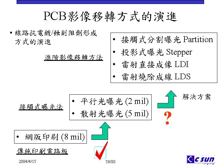
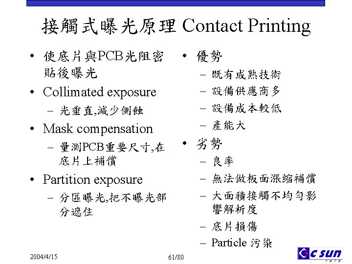
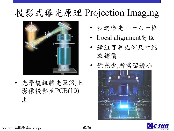
進階影像移轉解決方案 • Optical Exposure Technology • • Contact Printing 接觸式曝光 • – Collimated exposure – Mask compensation (sorting) – Partition exposure • Projection Imaging 投 影式曝光 • – Step and repeat – Step and scan – Laser projection imaging – Projection with dynamic mask 2004/4/15 60/80 Laser Scanning Technology (Non-Optics Technology) Laser Direct Imaging 雷射直接成像 – Laser direct imaging – Thermal laser direct imaging Laser Ablation 雷射燒除成線 – Laser structuring – Laser patterning
平行光曝光系統 Collimated Exposure 積光器 (Integrator) 反射鏡 (Reflection Mirror) 冷鏡 (Dichroic Mirror) 曝光照射面 (Exposure Surface) 橢圓集光器 (Collector) 點光源短弧燈 (Short Arc Lamp) 平行反射鏡 (Collimation Mirror) • 平行光源: 5 KW汞氙短弧燈 • 平行半角(CHA): 1. 5 • 斜射角(DA) < 1 2004/4/15 62/80
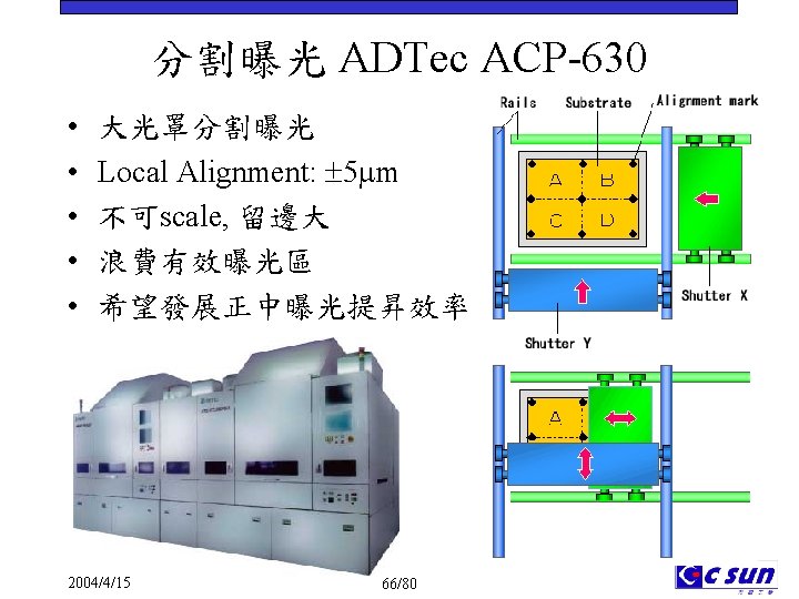
分割曝光 ADTec SRP-600 • 小光罩分割曝光 – 4~16 steps • L/S 20 m • Alignment: 2 m • 正中曝光 2004/4/15 • CCD cameras for alignment retract prior to exposure. • Stage 1 is an alignment stage with movable X, Y, and θ. • Stage 2 is a step & repeat stage with movable X and Y. 65/80
Step & Repeat曝光機 Ushio UX-5038 • 曝光 Step & Repeat – – • 解析度 光源 2 KW Short Arc – L/S : 12 m 曝光強度 35 mw/cm 2 – Do. F: 50 m 均勻度 5% • 對準度 曝光面積: 正方, – On-axis 2 CCD alignment Max. 141 x 141 mm – Overlay accuracy: 6. 5 m – Scaling: 1000 ppm 2004/4/15 Source: www. ushio. co. jp 69/80
Step & Scan曝光機 Tamarak Model 302 • 曝光 Scanning – – • 解析度: 光源 1 KW Short Arc – L/S: 4 m 曝光強度 40 mw/cm 2 – Do. F: 30 m 均勻度 3% • 對準度 Scan面積: 長 – Alignment 精度: 2 m 方 200 mm 2004/4/15 Source: www. tamsci. com 70/80
雷射投影成像 Laser Projection Imaging • Anvik Hex. Scan 2100 SPE – Excimer UV Laser 351 nm, 45~75 mw/cm 2 – Hex. Scan 40 x 40 mm 拼圖 – 投影至光阻上掃描曝光 – 線路 structuring • 解析度 – L/S: 10/10 m • 對準度 – Accuracy: 2. 5 m • 產能 2004/4/15 71/80 – 120 pnl/hr
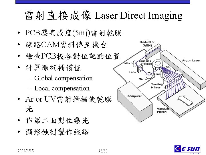
Projection with Dynamic Mask • Ball semiconductor (Japan) • TI 2004/4/15 72/80
LDI設備發展現況 2004/4/15 75/80
雷射成線系統 Laser Direct Structuring • Siemens Microbeam系統 • 直接用Laser掃描,依照 程資料將PCB表面錫 抗蝕刻阻劑燒除,再蝕刻後完成線路 • 適用用於IC Substrate、HDI PCB、Lead Frame 局部細線路製作 • 雷射源 – Nd doped, 1064 nm, diode pump – UV 532 nm, 355 nm • 解析度 – L/S - 50/50 m • 對準度 – Accuracy: 10 m 2004/4/15 Source: www. pl. siemens. de 77/80
雷射直接成線製程 • 全板鍍銅 Plate Cu – 10~15 m • 線路蝕刻 Etch Cu • 全板浸鍍錫 Immersion • 剝錫 Strip Tin – Etch resist – 1 m Tin • 表面處理 Surface Finish • 燒掉線路間錫材 Laser ablation Tin – 1000 mm/sec 2004/4/15 Source: www. pl. siemens. de 78/80
雷射成線 Laser Patterning • LPKF Micro. Line Drill 600 – THG UV Laser 355 nm – Scan 60 x 60 mm – 直接燒除銅層 • 用途 – 線路 structuring – 綠漆 structuring – 雷射鑽孔 • 解析度 – L: 20 m • 對準度 2004/4/15 Source: www. lpkfusa. com 79/80 – Accuracy: 15 m