Hardware Design of High Speed Switch Fabric IC

Hardware Design of High Speed Switch Fabric IC
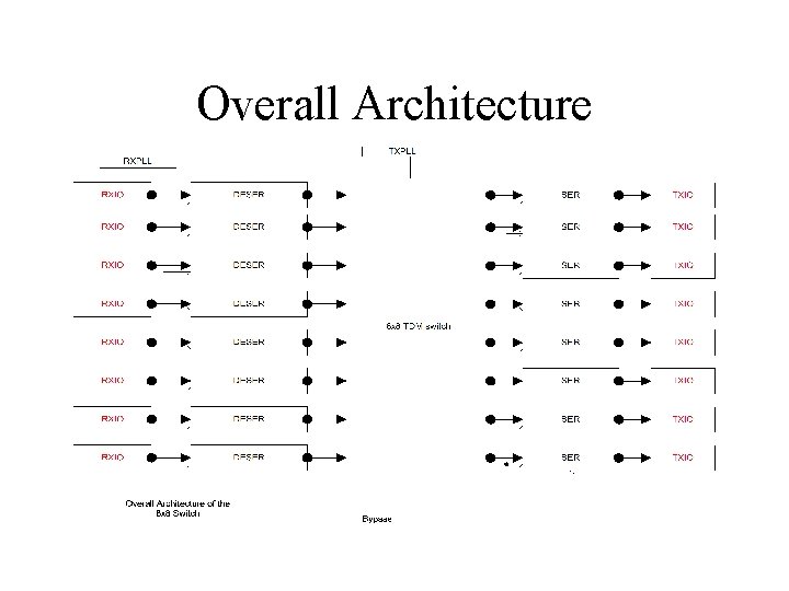
Overall Architecture
Features • Supports protocol-independent switching. Data are encapsulated in switching packets across the fabric. • Switching packet size is 64 bytes • Supports 8 x 8 switch with each port up to 2. 56~3. 2 Gbps • Supports scalable multichip switching
Features • 2. 56~3. 2 Gbps I/O: --CML IO driver --Embedded SERDES --Integrated CDR
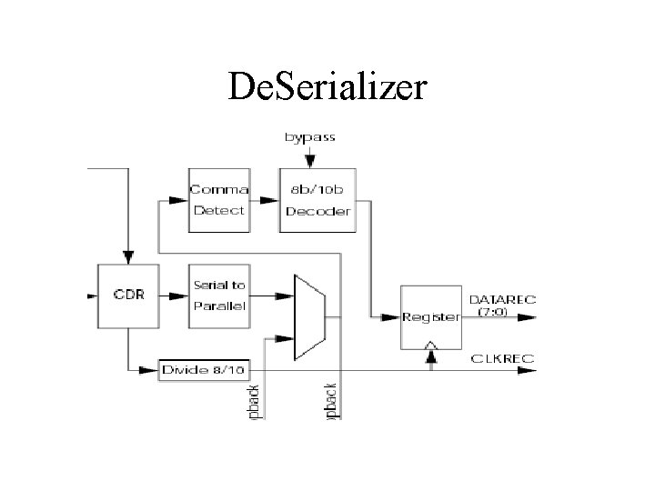
De. Serializer
De. Serializer • Converts the CML differential input to single bit input data through input CML buffer • Converts the single bit input data at 2. 56~3. 2 Gbps rate into 16/20 bit data bus at 160 MHz clock rate • Input reference clock 160 MHz • RX CML(clock multiplying unit) produces 1. 281. 6 GHz clock for data recovery from external 160 MHz clock
De. Serializer • Input reference clock 160 MHz • CDR(Clock Data Recovery) block produces 1. 281. 6 GHz clock for data recovery from external 160 MHz clock and input data • Front End receiver use recovered clock to sample and de-multiplexing single input data to 4 bit data bus at 640 MHz clock • Use 4 to 16/20 DEMUX to produce 16/20 bit data bus at 160 MHz
De. Serializer • Comma detector to detect comma word to align data byte boundary • Use 8/10 bit decoder to decode start of packet(SOP), destination port and data
8 x 8 TDM switch
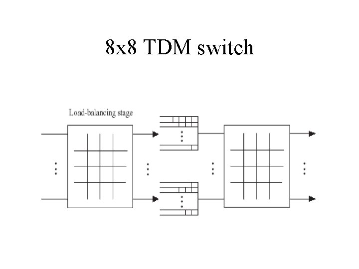
8 x 8 TDM switch • Performs the first stage load balanced traffic redistribution after the input FIFO queue • Input to first stage switch is consecutive 64 byte packet at each input port • Outputs of first stage switch include data, data valid, destination port, and sequence ID
8 x 8 TDM switch • Performs the second stage Birkhoff-von. Neumann switch after the resequence and output buffer queue • Input to second stage switch is distributive data from resequence and output buffer queue • Outputs of second stage switch include data, start of packet, and destination port
8 x 8 TDM switch • Operates at 160 MHz clock with clock period 6. 2 ns • For 2. 56 Gbps(64 bytes/packet)= 5 Mpackets/s • 200 ns/packet operation time(time slot)=32 cycles for 160 MHz
Serializer • Performs 16/20 b encoding function • Parallel to serial conversion convert 20/16 bit data bus at 160 MHz to single bit output at 2. 56~3. 2 Gbps • Differential CML output
PLL • TXPLL to generate 160 MHz clock for digital core • TXPLL to generate reference 160 MHz clock for synthesizing 1. 28~1. 6 GHz clock for serializer • RXPLL to generate 1. 28~1. 6 GHz clock for CDR from external 160 MHz clock
Tasks • PLLTR--PLL(TX and RX) design and Hspice simulation • DESER--De. Serializer(CDR) design and Hspice simulation • SWH-8 x 8 TDM switch design, synthesis, place and route, and verification • CCODEC--Comma detect and 8/10 b decoder, 8/10 b encoder
Tasks • SERCML—Serializer and CML high speed IO buffer design and Hspice simulation • APRD—Analog customized layout for DERSER • APRS-- Analog customized layout for SER and driver • Full chip integration and verification • Architecture specs
- Slides: 16