Hardware Architectures for Deep Learning Andrew Ling Ph
![CPU activity, step by step R 0 Load Mem[100] R 1 Load Mem[101] R CPU activity, step by step R 0 Load Mem[100] R 1 Load Mem[101] R](https://slidetodoc.com/presentation_image/7d8b0e5895728e662db3d8d7f6273d2b/image-13.jpg)
![Unroll the CPU hardware… R 0 Load Mem[100] R 1 Load Mem[101] R 2 Unroll the CPU hardware… R 0 Load Mem[100] R 1 Load Mem[101] R 2](https://slidetodoc.com/presentation_image/7d8b0e5895728e662db3d8d7f6273d2b/image-15.jpg)
![… and specialize by position R 0 Load Mem[100] R 1 Load Mem[101] R … and specialize by position R 0 Load Mem[100] R 1 Load Mem[101] R](https://slidetodoc.com/presentation_image/7d8b0e5895728e662db3d8d7f6273d2b/image-16.jpg)
![… and specialize R 0 Load Mem[100] R 1 Load Mem[101] R 2 Load … and specialize R 0 Load Mem[100] R 1 Load Mem[101] R 2 Load](https://slidetodoc.com/presentation_image/7d8b0e5895728e662db3d8d7f6273d2b/image-17.jpg)
![… and specialize R 0 Load Mem[100] R 1 Load Mem[101] R 2 Load … and specialize R 0 Load Mem[100] R 1 Load Mem[101] R 2 Load](https://slidetodoc.com/presentation_image/7d8b0e5895728e662db3d8d7f6273d2b/image-18.jpg)
![… and specialize R 0 Load Mem[100] R 1 Load Mem[101] 1. 2. 3. … and specialize R 0 Load Mem[100] R 1 Load Mem[101] 1. 2. 3.](https://slidetodoc.com/presentation_image/7d8b0e5895728e662db3d8d7f6273d2b/image-19.jpg)
![… and specialize R 0 Load Mem[100] R 1 Load Mem[101] 1. 2. 3. … and specialize R 0 Load Mem[100] R 1 Load Mem[101] 1. 2. 3.](https://slidetodoc.com/presentation_image/7d8b0e5895728e662db3d8d7f6273d2b/image-20.jpg)
![… and specialize R 0 Load Mem[100] R 1 Load Mem[101] R 2 Load … and specialize R 0 Load Mem[100] R 1 Load Mem[101] R 2 Load](https://slidetodoc.com/presentation_image/7d8b0e5895728e662db3d8d7f6273d2b/image-21.jpg)


- Slides: 43

Hardware Architectures for Deep Learning Andrew Ling, Ph. D. – Engineering Manager Machine Learning Acceleration Open. CL and the Open. CL logo are trademarks of Apple Inc.

Disclaimer Performance tests and ratings are measured using specific computer systems and/or components and reflect the approximate performance of Intel products as measured by those tests. Any difference in system hardware or software design or configuration may affect actual performance. Buyers should consult other sources of information to evaluate the performance of systems or components they are considering purchasing. For more information on performance tests and on the performance of Intel products, visit Intel Performance Benchmark Limitations. Some Results have been simulated and are provided for informational purposes only. Results were derived using simulations run on an architecture simulator. Any difference in system hardware or software design or configuration may affect actual performance. Intel does not control or audit the design or implementation of third party benchmarks or websites referenced in this document. Intel encourages all of its customers to visit the referenced websites or others where similar performance benchmarks are reported and confirm whether the referenced benchmarks are accurate and reflect performance of systems available for purchase. 2

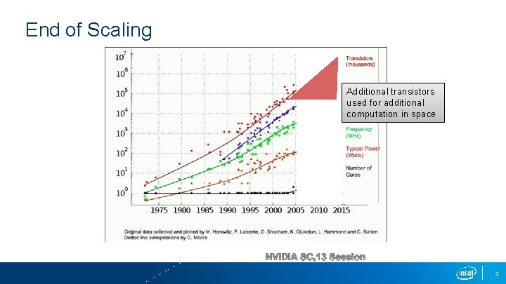
End of Scaling Additional transistors used for additional computation in space 3

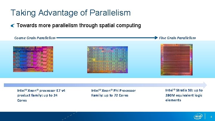
Taking Advantage of Parallelism Towards more parallelism through spatial computing Coarse Grain Parallelism CPUs Intel® Xeon® processor E 7 v 4 product family: up to 24 Cores Fine Grain Parallelism Multi-Cores Intel® Xeon® Phi Processor Family: up to 72 Cores FPGAs Intel® Stratix 10: up to 280 M equivalent logic elements 4

Temporal vs Spatial

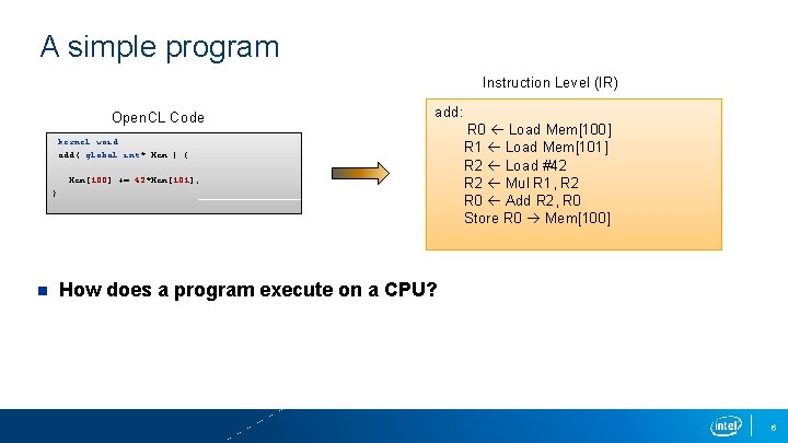
A simple program Instruction Level (IR) Open. CL Code kernel void add( global int* Mem ) {. . . Mem[100] += 42*Mem[101]; } n add: R 0 Load Mem[100] R 1 Load Mem[101] R 2 Load #42 R 2 Mul R 1, R 2 R 0 Add R 2, R 0 Store R 0 Mem[100] How does a program execute on a CPU? 6

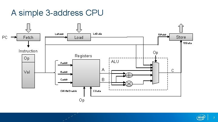
A simple 3 -address CPU PC Fetch Ld. Addr Load Ld. Data St. Addr Store St. Data Instruction Op Aaddr Val Op Registers ALU A A Baddr C B Caddr CWrite. Enable CData Op 7

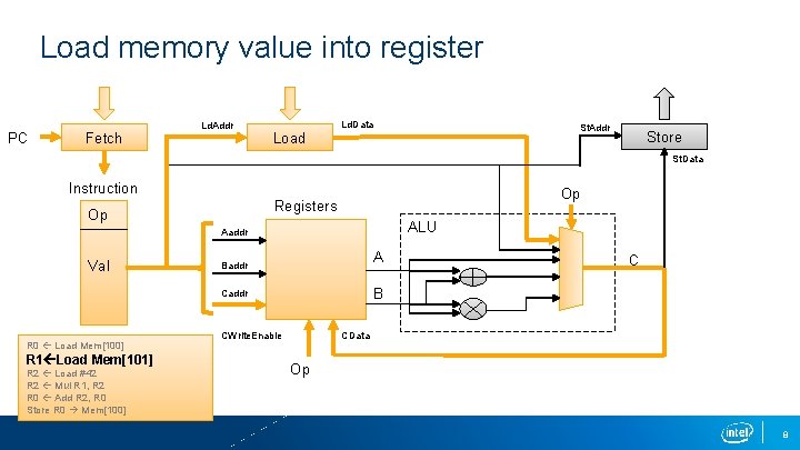
Load memory value into register PC Fetch Ld. Addr Load Ld. Data St. Addr Store St. Data Instruction Op Aaddr Val Op Registers ALU A A Baddr B Caddr R 0 Load Mem[100] R 1 Load Mem[101] R 2 Load #42 R 2 Mul R 1, R 2 R 0 Add R 2, R 0 Store R 0 Mem[100] C CWrite. Enable CData Op 8

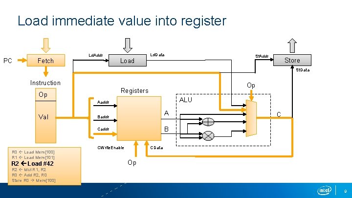
Load immediate value into register PC Fetch Ld. Addr Load Ld. Data St. Addr Store St. Data Instruction Op Aaddr Val Op Registers ALU A A Baddr B Caddr R 0 Load Mem[100] R 1 Load Mem[101] R 2 Load #42 C CWrite. Enable CData Op R 2 Mul R 1, R 2 R 0 Add R 2, R 0 Store R 0 Mem[100] 9

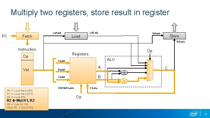
Multiply two registers, store result in register PC Fetch Ld. Addr Load Ld. Data St. Addr Store St. Data Instruction Op Aaddr Val Op Registers ALU A A Baddr B Caddr R 0 Load Mem[100] R 1 Load Mem[101] R 2 Load #42 R 2 Mul R 1, R 2 C CWrite. Enable CData Op R 0 Add R 2, R 0 Store R 0 Mem[100] 10

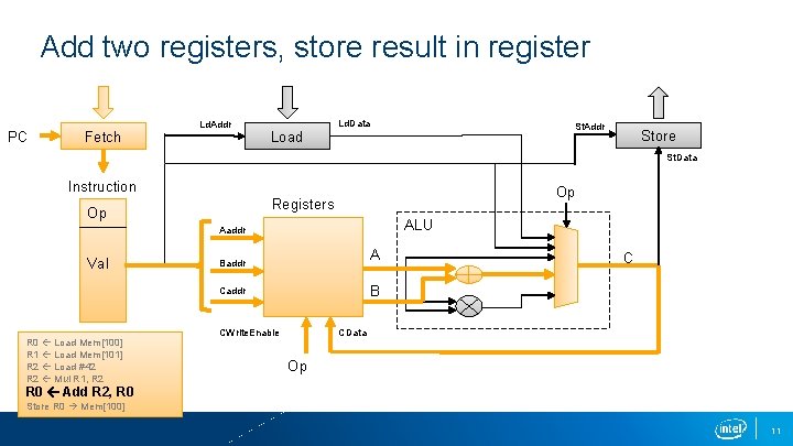
Add two registers, store result in register PC Fetch Ld. Addr Load Ld. Data St. Addr Store St. Data Instruction Op Aaddr Val Op Registers ALU A A Baddr B Caddr R 0 Load Mem[100] R 1 Load Mem[101] R 2 Load #42 R 2 Mul R 1, R 2 C CWrite. Enable CData Op R 0 Add R 2, R 0 Store R 0 Mem[100] 11

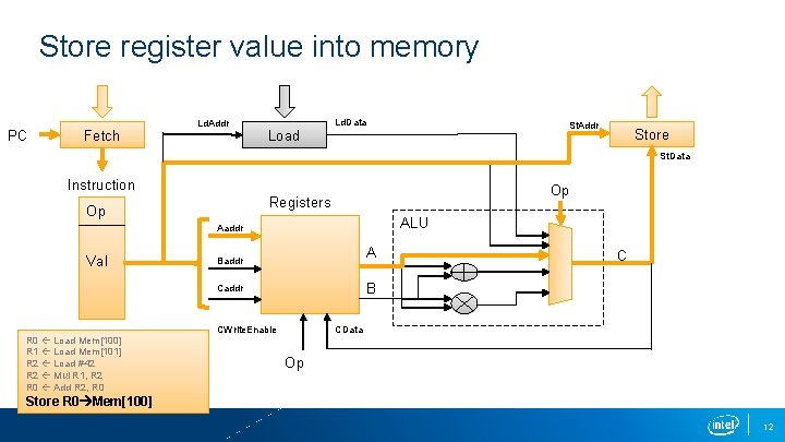
Store register value into memory PC Fetch Ld. Addr Load Ld. Data St. Addr Store St. Data Instruction Op Aaddr Val Op Registers ALU A A Baddr B Caddr R 0 Load Mem[100] R 1 Load Mem[101] R 2 Load #42 R 2 Mul R 1, R 2 R 0 Add R 2, R 0 C CWrite. Enable CData Op Store R 0 Mem[100] 12
![CPU activity step by step R 0 Load Mem100 R 1 Load Mem101 R CPU activity, step by step R 0 Load Mem[100] R 1 Load Mem[101] R](https://slidetodoc.com/presentation_image/7d8b0e5895728e662db3d8d7f6273d2b/image-13.jpg)
CPU activity, step by step R 0 Load Mem[100] R 1 Load Mem[101] R 2 Load #42 R 2 Mul R 1, R 2 R 0 Add R 2, R 0 Store R 0 Mem[100] A Time A A A 13

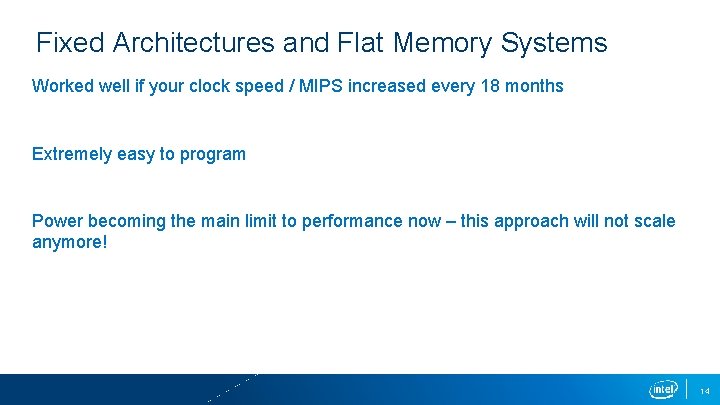
Fixed Architectures and Flat Memory Systems Worked well if your clock speed / MIPS increased every 18 months Extremely easy to program Power becoming the main limit to performance now – this approach will not scale anymore! 14
![Unroll the CPU hardware R 0 Load Mem100 R 1 Load Mem101 R 2 Unroll the CPU hardware… R 0 Load Mem[100] R 1 Load Mem[101] R 2](https://slidetodoc.com/presentation_image/7d8b0e5895728e662db3d8d7f6273d2b/image-15.jpg)
Unroll the CPU hardware… R 0 Load Mem[100] R 1 Load Mem[101] R 2 Load #42 R 2 Mul R 1, R 2 R 0 Add R 2, R 0 Store R 0 Mem[100] A Space A A A 15
![and specialize by position R 0 Load Mem100 R 1 Load Mem101 R … and specialize by position R 0 Load Mem[100] R 1 Load Mem[101] R](https://slidetodoc.com/presentation_image/7d8b0e5895728e662db3d8d7f6273d2b/image-16.jpg)
… and specialize by position R 0 Load Mem[100] R 1 Load Mem[101] R 2 Load #42 R 2 Mul R 1, R 2 R 0 Add R 2, R 0 Store R 0 Mem[100] A 1. Instructions are fixed. Remove “Fetch” A A A 16
![and specialize R 0 Load Mem100 R 1 Load Mem101 R 2 Load … and specialize R 0 Load Mem[100] R 1 Load Mem[101] R 2 Load](https://slidetodoc.com/presentation_image/7d8b0e5895728e662db3d8d7f6273d2b/image-17.jpg)
… and specialize R 0 Load Mem[100] R 1 Load Mem[101] R 2 Load #42 R 2 Mul R 1, R 2 R 0 Add R 2, R 0 Store R 0 Mem[100] A 1. Instructions are fixed. Remove “Fetch” 2. Remove unused ALU ops A A A 17
![and specialize R 0 Load Mem100 R 1 Load Mem101 R 2 Load … and specialize R 0 Load Mem[100] R 1 Load Mem[101] R 2 Load](https://slidetodoc.com/presentation_image/7d8b0e5895728e662db3d8d7f6273d2b/image-18.jpg)
… and specialize R 0 Load Mem[100] R 1 Load Mem[101] R 2 Load #42 R 2 Mul R 1, R 2 R 0 Add R 2, R 0 Store R 0 Mem[100] A 1. Instructions are fixed. Remove “Fetch” 2. Remove unused ALU ops 3. Remove unused Load / Store A A A 18
![and specialize R 0 Load Mem100 R 1 Load Mem101 1 2 3 … and specialize R 0 Load Mem[100] R 1 Load Mem[101] 1. 2. 3.](https://slidetodoc.com/presentation_image/7d8b0e5895728e662db3d8d7f6273d2b/image-19.jpg)
… and specialize R 0 Load Mem[100] R 1 Load Mem[101] 1. 2. 3. 4. Instructions are fixed. Remove “Fetch” Remove unused ALU ops Remove unused Load / Store Wire up registers properly! And propagate state. R 2 Load #42 R 2 Mul R 1, R 2 R 0 Add R 2, R 0 Store R 0 Mem[100] 19
![and specialize R 0 Load Mem100 R 1 Load Mem101 1 2 3 … and specialize R 0 Load Mem[100] R 1 Load Mem[101] 1. 2. 3.](https://slidetodoc.com/presentation_image/7d8b0e5895728e662db3d8d7f6273d2b/image-20.jpg)
… and specialize R 0 Load Mem[100] R 1 Load Mem[101] 1. 2. 3. 4. Instructions are fixed. Remove “Fetch” Remove unused ALU ops Remove unused Load / Store Wire up registers properly! And propagate state. 5. Remove dead data. R 2 Load #42 R 2 Mul R 1, R 2 R 0 Add R 2, R 0 Store R 0 Mem[100] 20
![and specialize R 0 Load Mem100 R 1 Load Mem101 R 2 Load … and specialize R 0 Load Mem[100] R 1 Load Mem[101] R 2 Load](https://slidetodoc.com/presentation_image/7d8b0e5895728e662db3d8d7f6273d2b/image-21.jpg)
… and specialize R 0 Load Mem[100] R 1 Load Mem[101] R 2 Load #42 1. 2. 3. 4. Instructions are fixed. Remove “Fetch” Remove unused ALU ops Remove unused Load / Store Wire up registers properly! And propagate state. 5. Remove dead data. 6. Reschedule! R 2 Mul R 1, R 2 R 0 Add R 2, R 0 Store R 0 Mem[100] 21

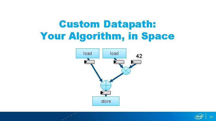
Custom Datapath: Your Algorithm, in Space load 42 store 22

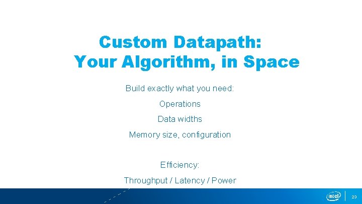
Custom Datapath: Your Algorithm, in Space Build exactly what you need: Operations Data widths Memory size, configuration Efficiency: Throughput / Latency / Power 23

Rise of Deep learning

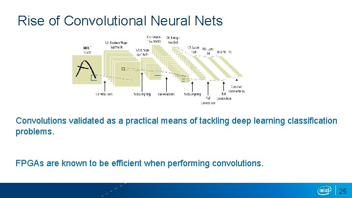
Rise of Convolutional Neural Nets Convolutions validated as a practical means of tackling deep learning classification problems. FPGAs are known to be efficient when performing convolutions. 25

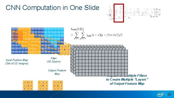
CNN Computation in One Slide -1 -1 9 -1 -1 Input Feature Map (Set of 2 D Images) Filter (3 D Space) Output Feature Map -1 3 -1 1 -1 -1 3 -1 -2 -1 -1 5 -1 4 7 -1 -1 -1 0 -1 Repeat for Multiple Filters to Create Multiple “Layers” of Output Feature Map 26

A Brief Introduction to FPGAs

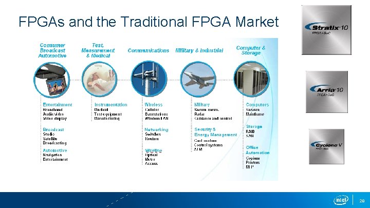
FPGAs and the Traditional FPGA Market 28

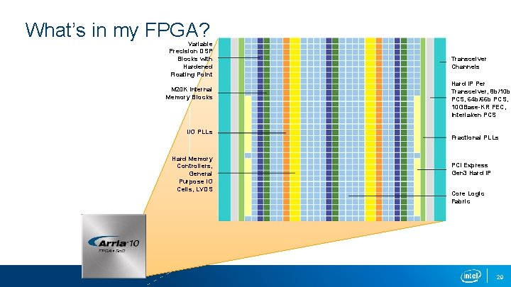
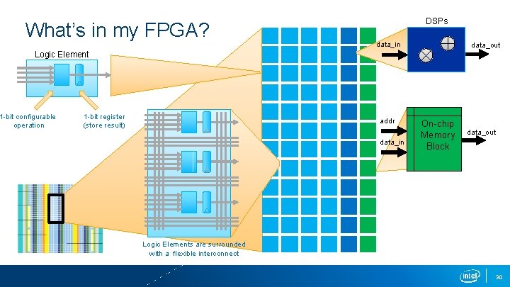
What’s in my FPGA? Variable Precision DSP Blocks with Hardened Floating Point M 20 K Internal Memory Blocks I/O PLLs Hard Memory Controllers, General Purpose IO Cells, LVDS Transceiver Channels Hard IP Per Transceiver, 8 b/10 b PCS, 64 b/66 b PCS, 10 GBase-KR FEC, Interlaken PCS Fractional PLLs PCI Express Gen 3 Hard IP Core Logic Fabric 29

What’s in my FPGA? DSPs data_in data_out Logic Element 1 -bit configurable operation 1 -bit register (store result) addr data_in On-chip Memory Block data_out Logic Elements are surrounded with a flexible interconnect 30

A Case for FPGA Acceleration: Deep Learning

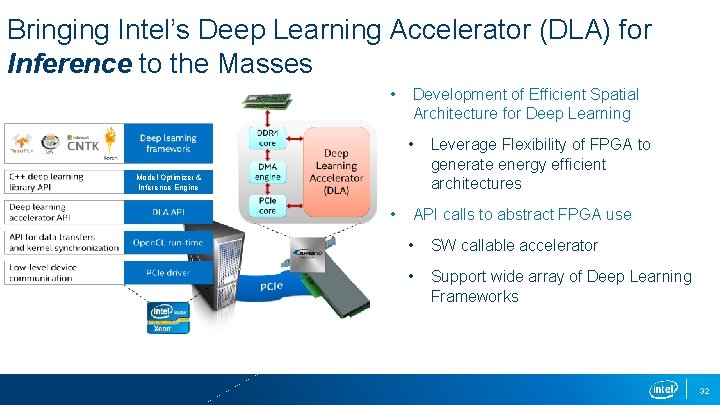
Bringing Intel’s Deep Learning Accelerator (DLA) for Inference to the Masses • Development of Efficient Spatial Architecture for Deep Learning • Model Optimizer & Inference Engine • Leverage Flexibility of FPGA to generate energy efficient architectures API calls to abstract FPGA use • SW callable accelerator • Support wide array of Deep Learning Frameworks 32

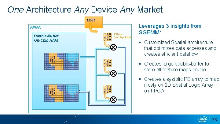
One Architecture Any Device Any Market DDR FPGA Double-Buffer On-Chip RAM 123 456 789 1 2 3 4 5 6 7 8 9 Filters Leverages 3 insights from SGEMM: (on-chip RAM) § Customized Spatial architecture that optimizes data accesses and creates efficient dataflow § Creates large double-buffer to store all feature maps on-die § Creates a systolic PE array to map nicely on 2 D Spatial Logic Array on FPGA 33

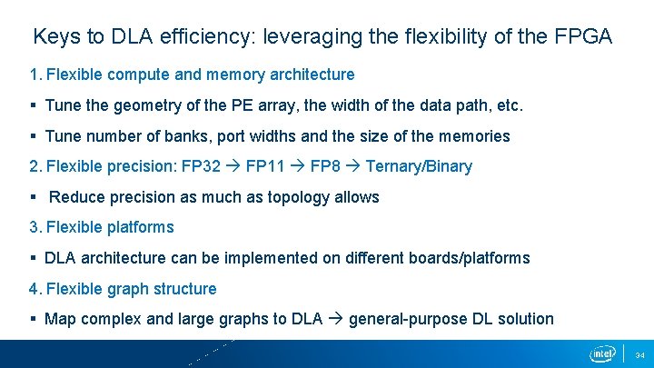
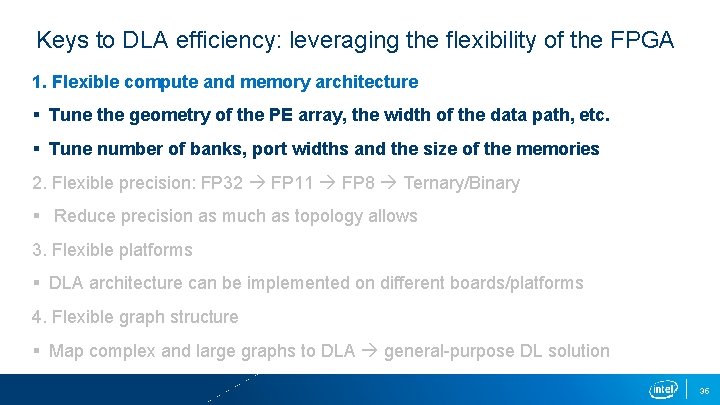
Keys to DLA efficiency: leveraging the flexibility of the FPGA 1. Flexible compute and memory architecture § Tune the geometry of the PE array, the width of the data path, etc. § Tune number of banks, port widths and the size of the memories 2. Flexible precision: FP 32 FP 11 FP 8 Ternary/Binary § Reduce precision as much as topology allows 3. Flexible platforms § DLA architecture can be implemented on different boards/platforms 4. Flexible graph structure § Map complex and large graphs to DLA general-purpose DL solution 34

Keys to DLA efficiency: leveraging the flexibility of the FPGA 1. Flexible compute and memory architecture § Tune the geometry of the PE array, the width of the data path, etc. § Tune number of banks, port widths and the size of the memories 2. Flexible precision: FP 32 FP 11 FP 8 Ternary/Binary § Reduce precision as much as topology allows 3. Flexible platforms § DLA architecture can be implemented on different boards/platforms 4. Flexible graph structure § Map complex and large graphs to DLA general-purpose DL solution 35

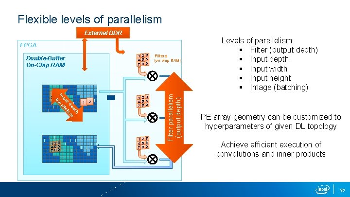
Flexible levels of parallelism External DDR FPGA th ep m t d lis pu lle In ara p 123 456 789 1 2 3 4 5 6 7 8 9 Filters (on-chip RAM) Filter parallelism (output depth) 1 2 3 4 5 6 7 8 9 Double-Buffer On-Chip RAM Levels of parallelism: § Filter (output depth) § Input depth § Input width § Input height § Image (batching) PE array geometry can be customized to hyperparameters of given DL topology Achieve efficient execution of convolutions and inner products 36

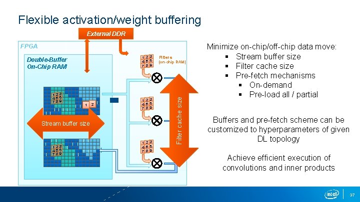
Flexible activation/weight buffering External DDR FPGA 123 456 789 1 2 3 4 5 6 7 8 9 Stream buffer size 123 456 789 1 2 3 4 5 6 7 8 9 Filters (on-chip RAM) Filter cache size 1 2 3 4 5 6 7 8 9 Double-Buffer On-Chip RAM Minimize on-chip/off-chip data move: § Stream buffer size § Filter cache size § Pre-fetch mechanisms § On-demand § Pre-load all / partial Buffers and pre-fetch scheme can be customized to hyperparameters of given DL topology Achieve efficient execution of convolutions and inner products 37

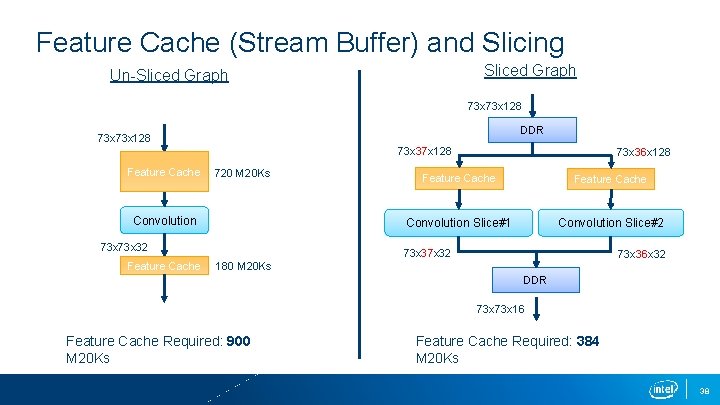
Feature Cache (Stream Buffer) and Slicing Sliced Graph Un-Sliced Graph 73 x 128 DDR 73 x 128 73 x 37 x 128 Feature Cache 720 M 20 Ks Convolution 73 x 32 Feature Cache 73 x 36 x 128 Feature Cache Convolution Slice#1 Convolution Slice#2 73 x 37 x 32 73 x 36 x 32 180 M 20 Ks DDR 73 x 16 Feature Cache Required: 900 M 20 Ks Feature Cache Required: 384 M 20 Ks 38

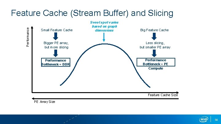
Performance Feature Cache (Stream Buffer) and Slicing Small Feature Cache Bigger PE array, but more slicing Performance Bottleneck = DDR Sweet spot varies based on graph dimensions Big Feature Cache Less slicing, but smaller PE array Performance Bottleneck = PE Compute Feature Cache Size PE Array Size 39

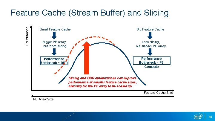
Performance Feature Cache (Stream Buffer) and Slicing Small Feature Cache Bigger PE array, but more slicing Less slicing, but smaller PE array Performance Bottleneck = PE Compute Performance Bottleneck = DDR Slicing and DDR optimizations can improve performance at smaller feature cache sizes, allowing for the PE array to be scaled up Feature Cache Size PE Array Size 40

Hardware / Software convergence

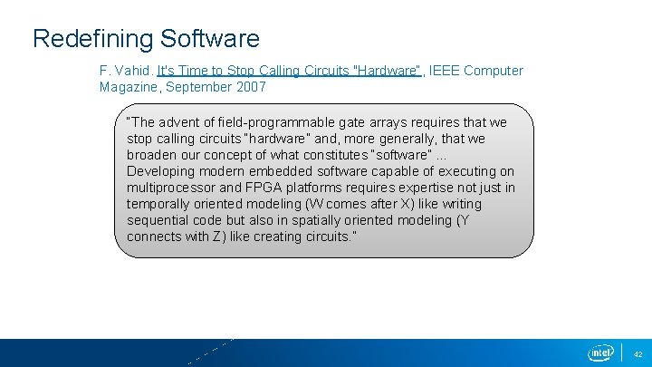
Redefining Software F. Vahid. It's Time to Stop Calling Circuits "Hardware“, IEEE Computer Magazine, September 2007 “The advent of field-programmable gate arrays requires that we stop calling circuits “hardware” and, more generally, that we broaden our concept of what constitutes “software”. . . Developing modern embedded software capable of executing on multiprocessor and FPGA platforms requires expertise not just in temporally oriented modeling (W comes after X) like writing sequential code but also in spatially oriented modeling (Y connects with Z) like creating circuits. ” 42
