
Guitar Signal Transmitter Project by Santiago Yeomans Chad
Guitar Signal Transmitter Project by Santiago Yeomans, Chad Cummins, Gboyega Adeola
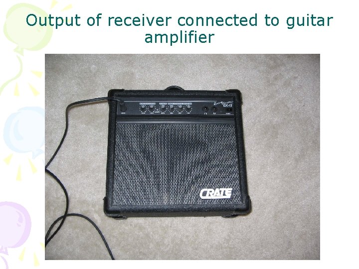
Introduction • Electric guitar output will connect to FM transmitter • Transmitted audio will be received at receiver and connected to guitar amplifier • ¼ “ audio plugs used for connections – output of guitar to transmitter – output of receiver to amp

Frequency Modulation vs. Phase Modulation FM PM Fair S/N ratio Best S/N ratio Variable modulation index Easier implementation VCO can produce high index freq. modulation Cost efficient Constant modulation index Phase lock loop to demodulate signal Multipliers needed to produce high index PM Expensive
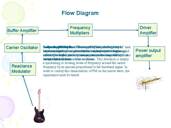
Flow Diagram Buffer Amplifier Carrier Oscillator Reactance Modulator Frequency Multipliers Power Output Reactance Buffer Frequency Amplifier: Modulator: Multipliers: Section. The buffer The Develops To avoid nature amplifier frequency the of FM final acts iscarrier as that drifts a high when power of the input the. LC to tank baseband impedance while be transmitted. modulating signal with. Also is a the low zero, included carrier gain the and carrier by here low theisbaseband output an at its impedance “carrier” impedance with amatching frequency, high associated whenit. it The with modulation network, peaks in which index, high theinput carrier the modulation output impedance deviation impedance can prevents take is at place aismaximum the loading atsame lower effects and asfrequencies that when from it troughs the with on the oscillator a higher load the (antenna) deviation section. Q factorisofatthe its oscillator. minimum. This deviation is simply a quickening or slowing down of frequency around the carrier frequency by an amount proportional to the baseband signal. In order to convey this characteristic of FM on the carrier wave, the capacitance must be varied. Driver Amplifier Power output amplifier
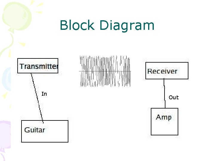
Block Diagram In Out
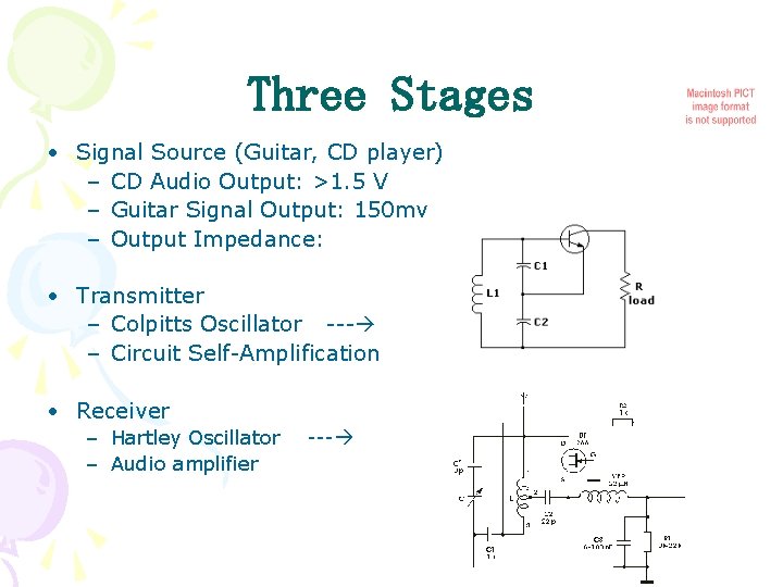
Three Stages • Signal Source (Guitar, CD player) – CD Audio Output: >1. 5 V – Guitar Signal Output: 150 mv – Output Impedance: • Transmitter – Colpitts Oscillator --- – Circuit Self-Amplification • Receiver – Hartley Oscillator – Audio amplifier ---
Oscillator Resonant Circuits. Resonant frequency is that at which the impedance of capacitor & inductor is the same; it represents the oscillator carrier frequency in Hertz. The parallel resonant circuit we used, known as an LC tank, takes the advantage of the resonant frequency and allows the impedance to be at a maximum & the current at a minimum at Fc. Q : ratio of maximum energy stored to the amount lost per ac cycle. It determines the 3 d. B bandwidth of resonant circuits. Since we didn’t have a resistor in the LC tank, the inherent properties of inductor & capacitor at high frequencies had to be taken into account.
Essential Circuit Elements • Transistors: – Transmitter: 2 (2 N 3904) – Receiver: BF 256, 2 N 3904 • Inductors – Copper Coils • 5 turns • 16 turns
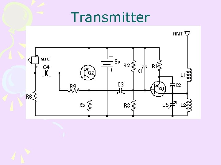
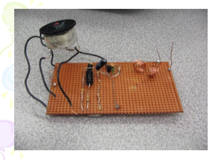
Transmitter
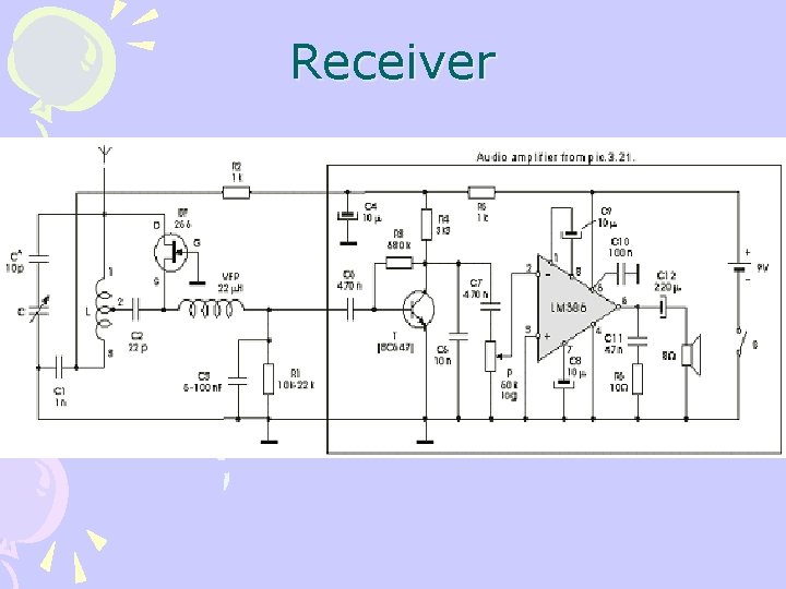
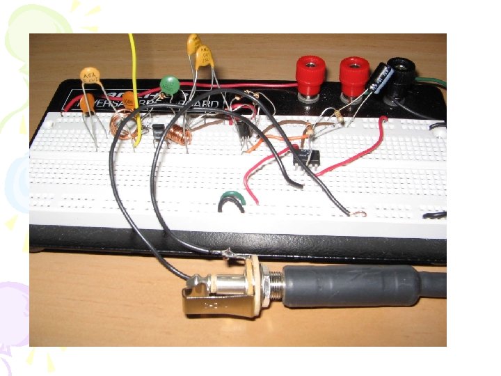
Receiver
6 -Band Equalization Stage Chebyshev Filters LPF 682 Hz 1 k. Hz
2 k. Hz 4 k. Hz
8 k. Hz 10. 9 k. Hz

Pspice Simulation
Output of receiver connected to guitar amplifier
Project Achievements • Achieved both FM RF Transmission and reception – Carrier frequency of 100 MHz • Audio received and sent to guitar amplifier • Audio from cd player worked well • Temporarily had guitar audio transmitting and receiving • Circuits were low cost to build
Performance • Quality of Audio – Clear at times, some noise occasionally • Transmission – Better transmission was achieved with a source device having a larger input impedance.
Project Challenges • Setup both transmitter and receiver for same carrier frequency (100 MHz) – Variable Capacitor range was unknown, not sure about the pins (Variable cap taken from $5 handheld radio bought from Wal-Mart)
Challenges continued • • • Working with the LM 741 Op Amp Working with a breadboard Parasitic Capacitances Unable to Effectively Simulate Inductors Parasitic Capacitances inherent in high frequency engineering
Oversights • Impedance Mismatching – Between Amplifier and Receiver • Under-estimated difficulty of amplifying guitar audio before transmission
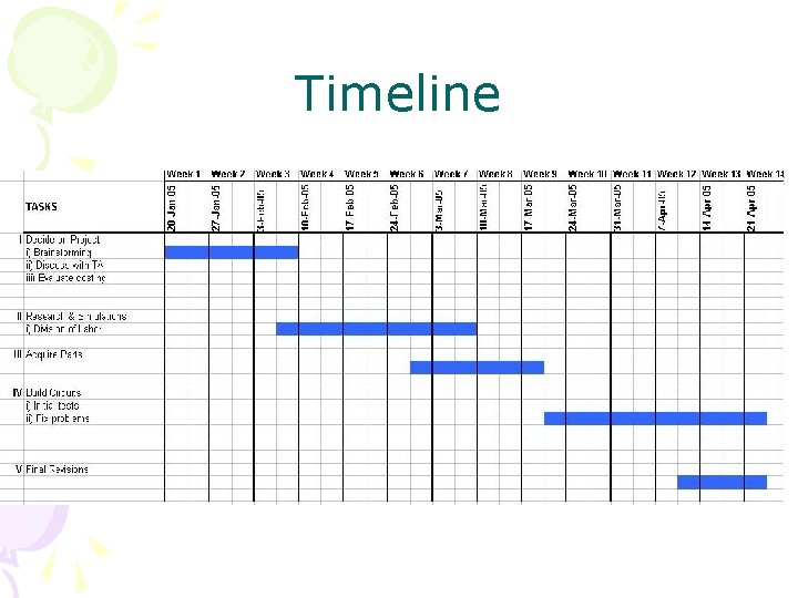
Timeline
Factors for obtaining better S/N Resistive properties in LC tank A) Skin effect - at high frequencies, there is less cross sectional area for carriers to move, so the resistance increase; when the magnetic field at the centre of the wire increases and local inductive reactance takes over, that is, stray capacitances begin to build up between adjacent turns. B) Dielectric permittivity Temperature Stability of the oscillator Components in oscillator have non-zero temperature coefficients. To find the change in frequency for a given temperature change, simply multiply the coefficient by the temperature change & the centre frequency. Major source of frequency instability: Capacitor & Transistor (junction capacitance) More compact circuitry Wrapping the circuit with aluminum foil to electromagnetically shield the RF stage. Unwanted electromagentic radiation had to be stopped from destructively interfering With the carrier modulation.
Future Improvements • Replace the common 2 N 3904 transistor with a BC 549 which would perform better with high frequency • Use a ground plane for better performance of sensitive circuits • Solder all connections
- Slides: 25