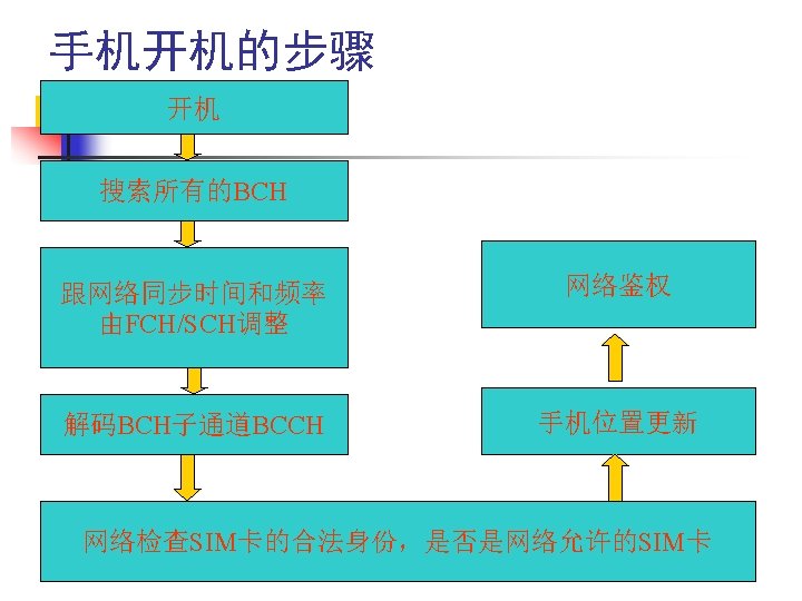
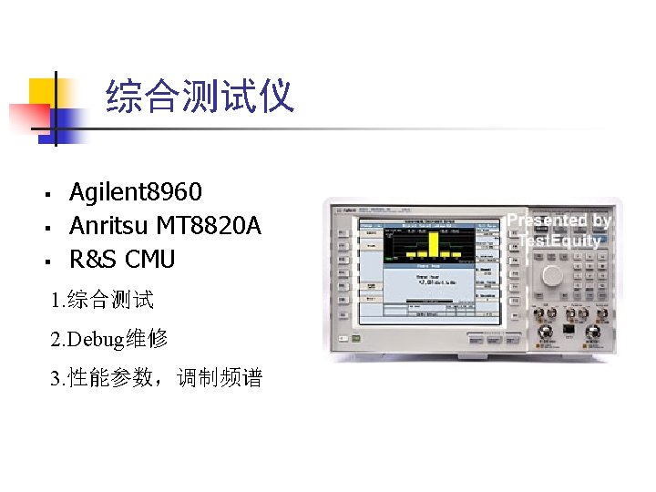
GSM n n n n GSM 900 FCH

 = 890 + (CH-1024)*0. 20")


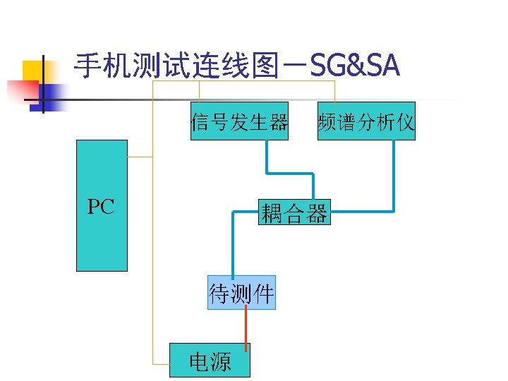
 § § Keithley 2304, 2306 Agilent 66311 B 1. 提供电压电流 2. sense的用途")
 § § § Agilent 4432 B Anritsu MG 3681 A R&S 1.")
 § § § Agilent 4405 B Advantest R 3267 R&S 1. 输出频谱")


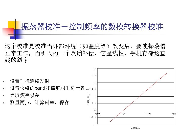
 Mid-Burst Power Level Ramp Down Ramp UP")
 Figure 3: Pm. W vs Element")
1/2=(0. 05*P)1/2=10^((Pd. Bm-13)/20) Pm. W(t)=(A-B)Sin 3(K*t)+B 其中 K=180/(2*T) TXP=m*V+c m=(TXPH-TXPL)/(VH-VL) c=TXPH-m*VH")


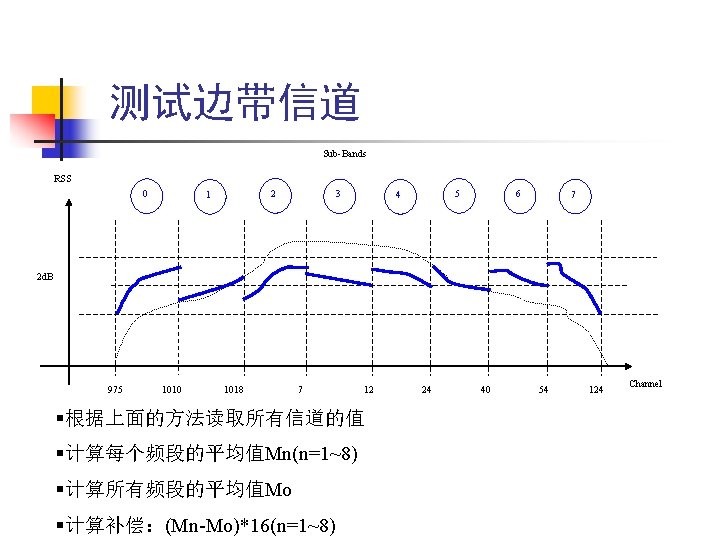


 §设置手机为 厂测试模式FTM 0 1 2 3 4 5 6 7 1017")
 执行GET_DVGA_OFFSET命令,保存结果")
和 NV_CDMA_LNA_FALL(-92. 2)中间值-90. 2,执行 GET_LNA_OFFSET命令,保存结果 设置信号发生器为NV_CDMA_LNA_2_RISE(-78. 2)和 NV_CDMA_LNA_2_FALL(-82. 2)中间值-80. 2,执行")


![Rx的频率补偿校准3 NV_CDMA_VGA_GAIN_OFFSET_VS_FREQ[i]= (Vga. Offset. Vs. Freq[i]-NV_CDMA_VGA_OFFSET)/12 § NV_CDMA_LNA_OFFSET_VS_FREQ[i]= Lna. Offset. Vs. Freq[i]-NV_LNA_RANGE_OFFSET § NV_CDMA_LNA_12_OFFSET_VS_FREQ[i]=](https://slidetodoc.com/presentation_image/7dc6ceaef312c45451bb1ebc490386f5/image-79.jpg "Rx的频率补偿校准3 NV_CDMA_VGA_GAIN_OFFSET_VS_FREQ[i]= (Vga. Offset. Vs. Freq[i]-NV_CDMA_VGA_OFFSET)/12 § NV_CDMA_LNA_OFFSET_VS_FREQ[i]= Lna. Offset. Vs. Freq[i]-NV_LNA_RANGE_OFFSET § NV_CDMA_LNA_12_OFFSET_VS_FREQ[i]=")

 用SET_PDM调节Tx_AGC_ADJ PDM接近功率点(48.")

 如果PA只有两种状态,则 NV_R 2_RISE/FALL, NV_R 3_RI SE/FALL设置为")
![计算方法 § § § CDMA_TX_LIN_MASTER_OFF_0=Cdma. Tx. Lin. Master. Off 0 ΣCDMA_TX_LIN_MASTER_SLP[i]=Cdma. Tx. Lin. Master.](https://slidetodoc.com/presentation_image/7dc6ceaef312c45451bb1ebc490386f5/image-89.jpg "计算方法 § § § CDMA_TX_LIN_MASTER_OFF_0=Cdma. Tx. Lin. Master. Off 0 ΣCDMA_TX_LIN_MASTER_SLP[i]=Cdma. Tx. Lin. Master.")
-768 Desired. Power. Limit= 24 d.")

- Slides: 94
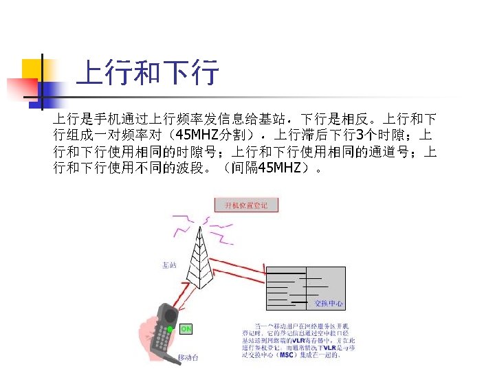
GSM 频段 n n n n GSM 900 F(CH) = 890 + (CH-1024)*0. 20 F(CH) = 890 + CH*0. 20 TX/RX Duplex : 45 MHz MS Tx 890 – 914. 8 MHz MS Rx 935 – 959. 8 MHz DCS Frequency Channel GSM 1800 F(CH) = 1710. 2 + (CH-512)*0. 20 TX/RX Duplex : 95 MHz PCS Frequency Channel GSM 1900 F(CH) = 1850. 2 + (CH-512)*0. 20 TX/RX Duplex : 80 MHz CH [955, 1023] CH [0, 124] CH [512, 885]
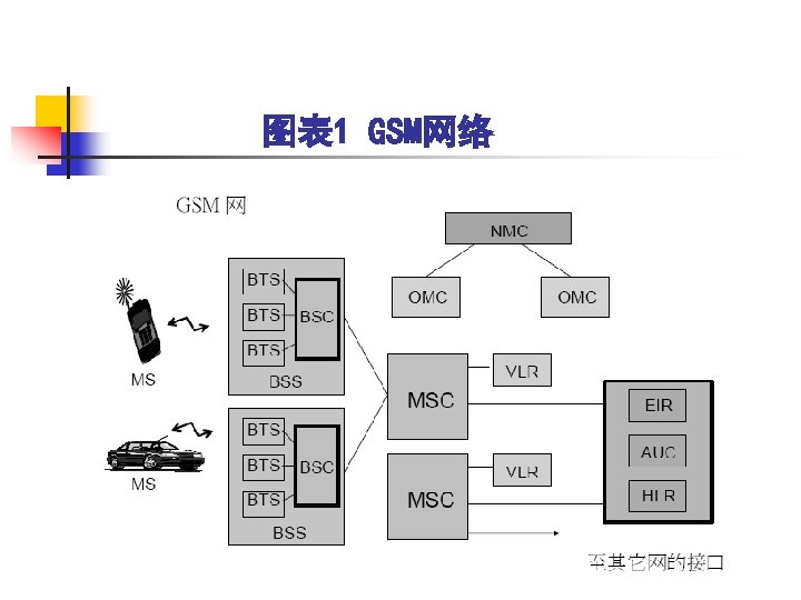
网络组成--其他 §TRAN----Trans coding/rate adapter unit速率适配器 §HLR----Home location register归属位置寄存器 §VLR----visiting location register访问位置寄存器 §AUC----Authentication center鉴权中心 §EIR----Equipment identify register装备身份中心 §BC----Billing center收费中心 §OMC----Operation and maintenance center操作运营中心 §SMSC----短信中心
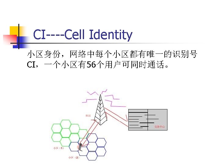
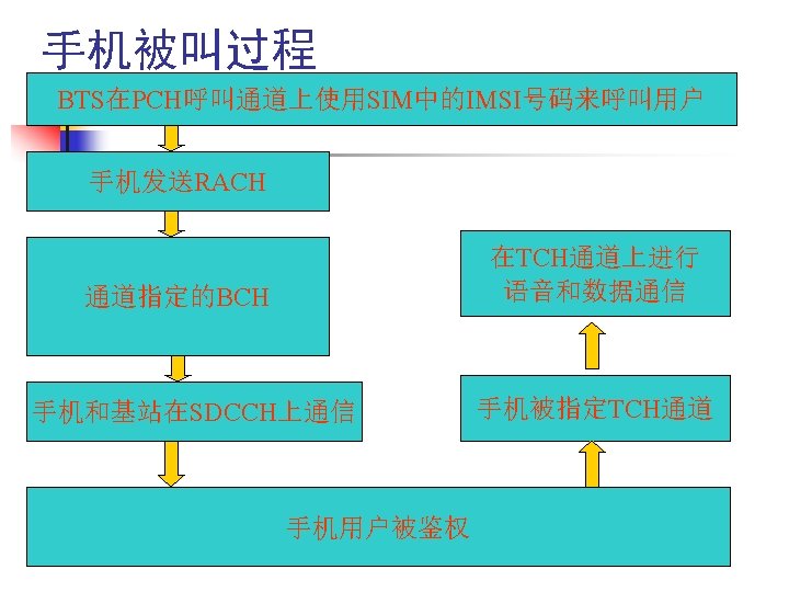
其他 § § IMEI:international mobile equipment identity国际移动设备识别号。 小区接入技术FDMA TDMA CDMA Timeslot 1 timeslot= 576. 92 us, 1 frame=8 timeslots 跳频
电源(Power supply) § § Keithley 2304, 2306 Agilent 66311 B 1. 提供电压电流 2. sense的用途 使测量更精确,消除路径损耗。
信号发生器(Signal Generator) § § § Agilent 4432 B Anritsu MG 3681 A R&S 1. 提供射频信号
频谱分析仪(spectrum analyzer) § § § Agilent 4405 B Advantest R 3267 R&S 1. 输出频谱 2. 测量功率 3. 观察谐波失真
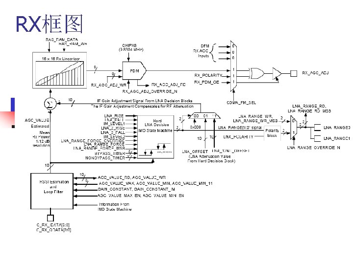
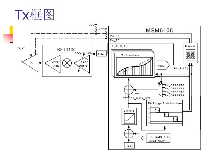
手机发射部分原理框图 Figure 1: Transmitter and Calibration CSP RF signal PA Power Ramp Registers DAC VAPC TXP NVM RAM LPF PM Calculate Ramp data sw. SW Measure Instrument
发射信号 Figure 2: Burst Shape Power(d. Bm) Mid-Burst Power Level Ramp Down Ramp UP Bit 0 Bit 147 Time(bits)
发射信号(部分) Figure 3: Pm. W vs Element
所用公式 V=(P*R)1/2=(0. 05*P)1/2=10^((Pd. Bm-13)/20) Pm. W(t)=(A-B)Sin 3(K*t)+B 其中 K=180/(2*T) TXP=m*V+c m=(TXPH-TXPL)/(VH-VL) c=TXPH-m*VH
测试步骤 Tx. PH推 VH推 Tx. PL推 VL推 M 0,c 0 Tx. PHreq VHreq PHreq Tx. PLreq VLreq PLreq
CDMA 校准方法 § For radio. One chipset § 以 6系列芯片为例
目录 n n 什么是RF校准 相关用语 准备 作 RX校准 n n n TX校准 n n n DVGA offset校准 LNA range offset校准 IM 2 频率相关校准 Tx linearizer Curve Rise Fall value 频率和温度关系的校准 Max limit power和HDET 其他
相关用语 n n n AGC: Automatic Gain Control自动增益控制 DMSS: Dual Mode Subscriber Software LNA Low Noise Amplifier低噪声放大器 NV Non-Volatile PDM Pulse Density Modulation IF Intermediate Frequency
频率信道的选择 §支持16信道的频率校准和补偿 §选择一个为基准信道(202) §设置手机为 厂测试模式FTM 0 1 2 3 4 5 6 7 1017 46 98 150 202 254 306 358 8 9 10 11 12 13 14 15 410 462 514 566 618 670 722 774
NV_CDMA_VGA_OFFSET § § 设置信号发生器发出NV_CDMA_LNA_FALL(92. 2 db) 执行GET_DVGA_OFFSET命令,保存结果
NV_LNA_RANGE_OFFSET § § 设置信号发生器为NV_CDMA_LNA_RISE(-88. 2)和 NV_CDMA_LNA_FALL(-92. 2)中间值-90. 2,执行 GET_LNA_OFFSET命令,保存结果 设置信号发生器为NV_CDMA_LNA_2_RISE(-78. 2)和 NV_CDMA_LNA_2_FALL(-82. 2)中间值-80. 2,执行 GET_LNA_OFFSET命令,保存结果 设置信号发生器为NV_CDMA_LNA_3_RISE(-59)和 NV_CDMA_LNA_3_FALL(-63)中间值-90. 2,执行 GET_LNA_OFFSET命令,保存结果 设置信号发生器为NV_CDMA_LNA_4_RISE(-45. 8)和 NV_CDMA_LNA_4_FALL(-49. 8)中间值-47. 8,执行 GET_LNA_OFFSET命令,保存结果
NV_LNA_RANGE_OFFSET 上面结果依次得到的是: NV_LNA_RANGE_OFFSET NV_LNA_RANGE_12_OFFSET NV_LNA_RANGE_3_OFFSET NV_LNA_RANGE_4_OFFSET
Rx的频率补偿校准1 § § § NV_CDMA_VGA_GAIN_OFFSET_VS_FREQ NV_CDMA_LNA_12_OFFSET_VS_FREQ NV_CDMA_LNA_3_OFFSET_VS_FREQ NV_CDMA_LNA_4_OFFSET_VS_FREQ
Rx的频率补偿校准3 NV_CDMA_VGA_GAIN_OFFSET_VS_FREQ[i]= (Vga. Offset. Vs. Freq[i]-NV_CDMA_VGA_OFFSET)/12 § NV_CDMA_LNA_OFFSET_VS_FREQ[i]= Lna. Offset. Vs. Freq[i]-NV_LNA_RANGE_OFFSET § NV_CDMA_LNA_12_OFFSET_VS_FREQ[i]= Lna 12 Offset. Vs. Freq[i]-NV_LNA_12_RANGE_OFFSET § NV_CDMA_LNA_3_OFFSET_VS_FREQ[i]= Lna 3 Offset. Vs. Freq[i]-NV_LNA_3_RANGE_OFFSET § NV_CDMA_LNA_4_OFFSET_VS_FREQ[i]= Lna 4 Offset. Vs. Freq[i]-NV_LNA_4_RANGE_OFFSET §
Tx校准项 § PA支持4个状态,每种状态包含自己的线性关系 § § § NV_CDMA_TX_LIN_MASTER 0 NV_CDMA_TX_LIN_MASTER 1 NV_CDMA_TX_LIN_MASTER 2 NV_CDMA_TX_LIN_MASTER 3 每个NV_CDMA_TX_LIN_MASTERx包含 37个数 据 § § CDMA_LIN_MASTER_OFF_0是第一个数据对应在 48. 4 d. Bm的PDM值 CDMA_TX_LIN_MASTER_SLP是各个功率等级的PDM 的差值
NV_CDMA_TX_LIN_MASTER 0 n n n 继续Rx的测试,不需要重新启动,确保在FTM模式 切换信道在基准信道 打开Tx发射,设置PA的状态(R 0= 0,R 1= 0) 用SET_PDM调节Tx_AGC_ADJ PDM接近功率点(48. 4, 45. 2,42,……-63. 6,-66. 8) 调节-60<point<26的点,其余的用线性公式推算出来 计算 n n NV_CDMA_TX_LIN_MASTER_OFF_0=TX_AGC_ADJ[0] NV_CDMA_TX_LIN_MASTER_SLP[n]=TX_AGC_ADJ[n+1]TX_AGC_ADJ[n]
功率等级 0 1 2 5 6 7 31 32 33 36 48. 4 45. 2 42 32. 4 29. 2 26 -50. 8 -54 -57. 2 -66. 8 0 0 0 37 50 63 382 395 434 0 0 0 13 13 13 14 13 13 13
校准PA_RISE/FALL § § 校准PA的特性 NV_R 1_RISE=2. 5*(PA_RISE+ 60) 如果PA只有两种状态,则 NV_R 2_RISE/FALL, NV_R 3_RI SE/FALL设置为 255 一般设置NV_R 1_RISE/FALL分 别为 185和175,表示RISE和 FALL的范围为 14 dbm和10 dbm
计算方法 § § § CDMA_TX_LIN_MASTER_OFF_0=Cdma. Tx. Lin. Master. Off 0 ΣCDMA_TX_LIN_MASTER_SLP[i]=Cdma. Tx. Lin. Master. Slp CDMA_TX_LIN_MASTER_OFF_0[n]=Cdma. Tx. Lin. Master. Off 0[n] ΣCDMA_TX_LIN_MASTER_SLP[i][n]=Cdma. Tx. Lin. Master. Slp [n] CDMA_TX_LIN_VS_TEMP[n]=Cdma. Tx. Lin. Master. Off 0[n]Cdma. Tx. Lin. Master. Off 0 CDMA_TX_SLP_VS_TEMP[n]=Cdma. Tx. Lin. Master. Slp[n]Cdma. Tx. Lin. Master. Slp
发射的最大功率和温度的关系 § § § NV_CDMA_LIM_VS_TEMP=10*(Desired. Power. Limit+ 60. 3)-768 Desired. Power. Limit= 24 d. Bm,因此 NV_CDMA_LIM_VS_TEMP为 75