Growth Structure and Pattern Formation for Thin Films

- Slides: 42

Growth, Structure and Pattern Formation for Thin Films Lecture 2. Structure Russel Caflisch Mathematics Department Materials Science and Engineering Department UCLA www. math. ucla. edu/~material U Tenn, 4/29/2007

Outline • Strain in epitaxial systems – Leads to structure – Quantum dots and their arrays • Atomistic strain model – Lattice statics model – Lattice mismatch • Numerical methods – Algebraic multigrid (AMG) – Artificial boundary conditions (ABC) • Application to nanowires – Step bunching instability • Summary U Tenn, 4/29/2007

Outline • Strain in epitaxial systems – Leads to structure – Quantum dots and their arrays • Atomistic strain model – Lattice statics model – Lattice mismatch • Numerical methods – Algebraic multigrid (AMG) – Artificial boundary conditions (ABC) • Application to nanowires – Step bunching instability • Summary U Tenn, 4/29/2007

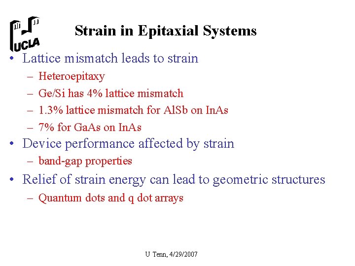
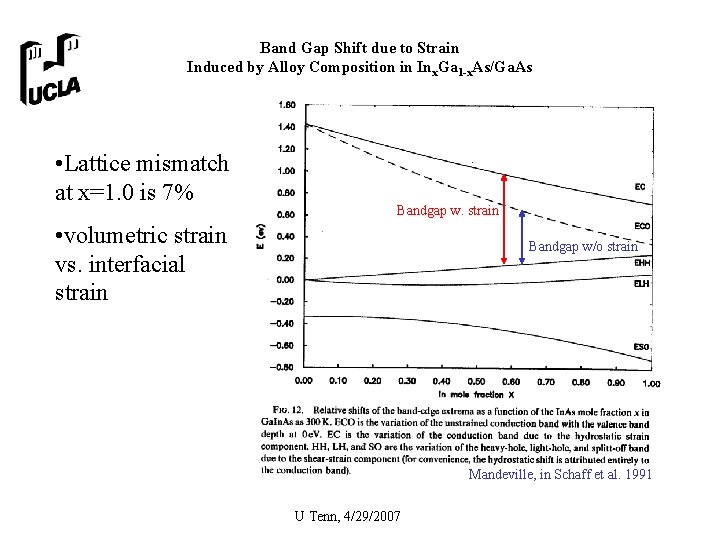
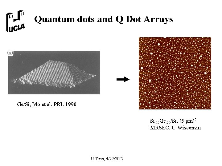
Strain in Epitaxial Systems • Lattice mismatch leads to strain – – Heteroepitaxy Ge/Si has 4% lattice mismatch 1. 3% lattice mismatch for Al. Sb on In. As 7% for Ga. As on In. As • Device performance affected by strain – band-gap properties • Relief of strain energy can lead to geometric structures – Quantum dots and q dot arrays U Tenn, 4/29/2007

Band Gap Shift due to Strain Induced by Alloy Composition in Inx. Ga 1 -x. As/Ga. As • Lattice mismatch at x=1. 0 is 7% Bandgap w. strain • volumetric strain vs. interfacial strain Bandgap w/o strain Mandeville, in Schaff et al. 1991 U Tenn, 4/29/2007

Quantum dots and Q Dot Arrays Ge/Si, Mo et al. PRL 1990 Si. 25 Ge. 75/Si, (5 μm)2 MRSEC, U Wisconsin U Tenn, 4/29/2007

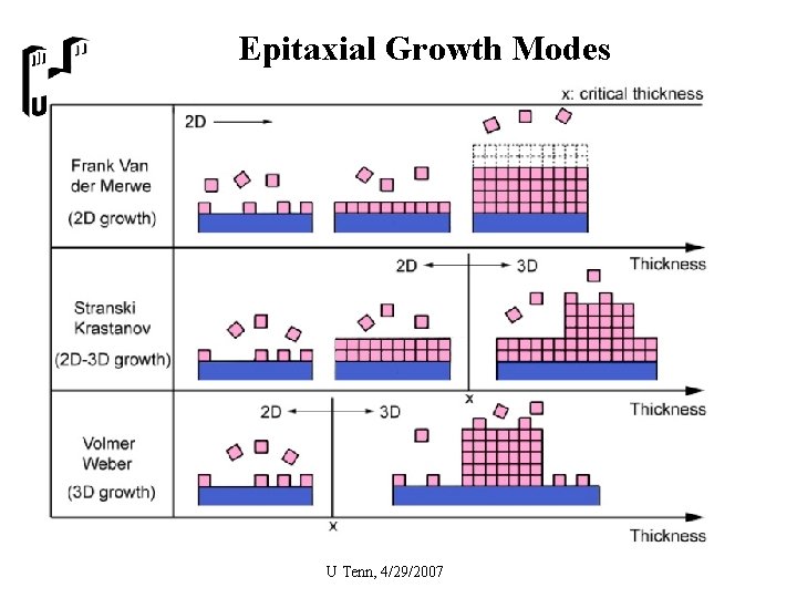
Epitaxial Growth Modes U Tenn, 4/29/2007

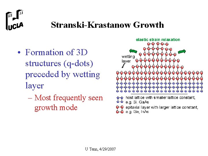
Stranski-Krastanow Growth • Formation of 3 D structures (q-dots) preceded by wetting layer – Most frequently seen growth mode U Tenn, 4/29/2007

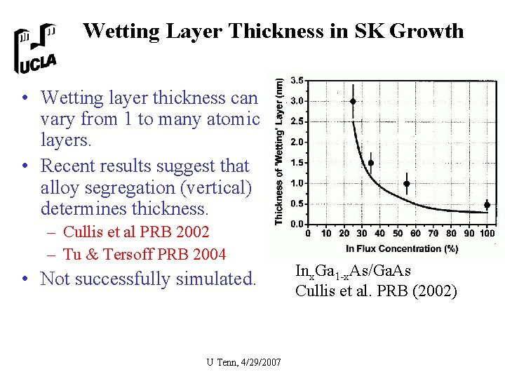
Wetting Layer Thickness in SK Growth • Wetting layer thickness can vary from 1 to many atomic layers. • Recent results suggest that alloy segregation (vertical) determines thickness. – Cullis et al PRB 2002 – Tu & Tersoff PRB 2004 • Not successfully simulated. U Tenn, 4/29/2007 Inx. Ga 1 -x. As/Ga. As Cullis et al. PRB (2002)

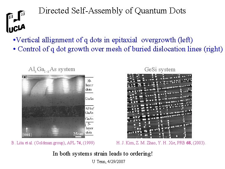
Directed Self-Assembly of Quantum Dots • Vertical allignment of q dots in epitaxial overgrowth (left) • Control of q dot growth over mesh of buried dislocation lines (right) Alx. Ga 1 -x. As system Ge. Si system B. Lita et al. (Goldman group), APL 74, (1999) H. J. Kim, Z. M. Zhao, Y. H. Xie, PRB 68, (2003). In both systems strain leads to ordering! U Tenn, 4/29/2007

Outline • Strain in epitaxial systems – Leads to structure – Quantum dots and their arrays • Strain model – Lattice statics model – Lattice mismatch • Numerical methods – Algebraic multigrid (AMG) – Artificial boundary conditions (ABC) • Application to nanowires – Step bunching instability • Summary U Tenn, 4/29/2007

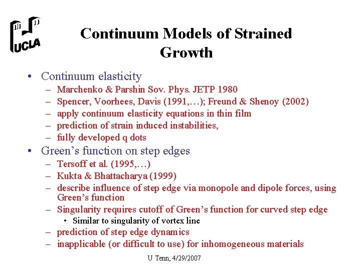
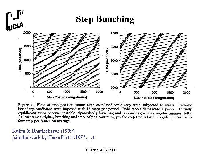
Continuum Models of Strained Growth • Continuum elasticity – – – Marchenko & Parshin Sov. Phys. JETP 1980 Spencer, Voorhees, Davis (1991, …); Freund & Shenoy (2002) apply continuum elasticity equations in thin film prediction of strain induced instabilities, fully developed q dots • Green’s function on step edges – Tersoff et al. (1995, …) – Kukta & Bhattacharya (1999) – describe influence of step edge via monopole and dipole forces, using Green’s function – Singularity requires cutoff of Green’s function for curved step edge • Similar to singularity of vortex line – prediction of step edge dynamics – inapplicable (or difficult to use) for inhomogeneous materials U Tenn, 4/29/2007

Step Bunching Kukta & Bhattacharya (1999) (similar work by Tersoff et al. 1995, …) U Tenn, 4/29/2007

Atomistic Modeling of Strain in Thin Films • Lattice statics for discrete atomistic system, – minimize discrete strain energy (Born & Huang, 1954) – Application to epitaxial films, • E. g. , Stewart, Pohland & Gibson (1994), Orr, Kessler, Snyder & Sander (1992), • Idealizations – Harmonic potentials, Simple cubic lattice – General, qualitative properties • Independent of system parameters – Computational speed enable additional physics & geometry • 3 D, alloying, surface stress • Atomistic vs. continuum – atomistic scale required for thin layer morphology • strain at steps – continuum scale required for efficiency • KMC requires small time steps, frequent updates of strain field U Tenn, 4/29/2007

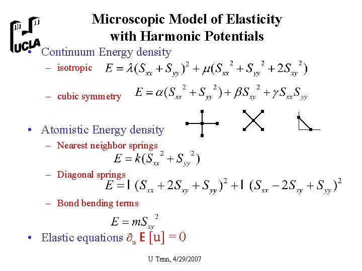
Microscopic Model of Elasticity with Harmonic Potentials • Continuum Energy density – isotropic – cubic symmetry • Atomistic Energy density – Nearest neighbor springs – Diagonal springs – Bond bending terms • Elastic equations u E [u] = 0 U Tenn, 4/29/2007

Cauchy Relations • Elasticity based on two-particle potentials → μ = 4 λ (Lame coefficients) for cubic symmetry – Cauchy relations • Access to full range of elasticity requires 3 body terms in energy – E. g. bond bending terms: (cos θ)2 – Keating model for Si consists of nearest neighbor springs and bond bending terms U Tenn, 4/29/2007 θ

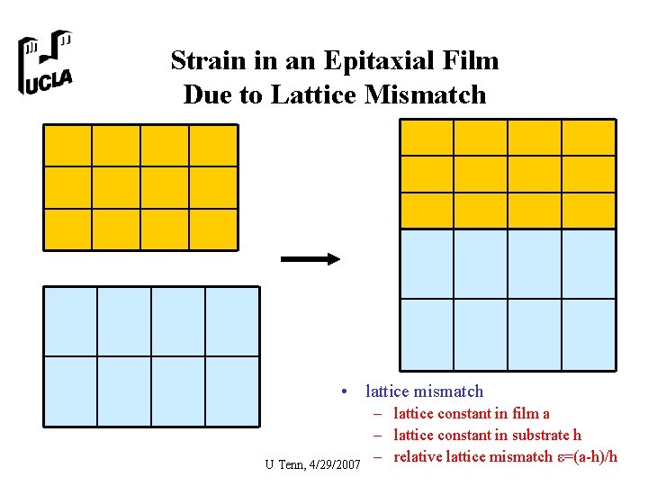
Strain in an Epitaxial Film Due to Lattice Mismatch • lattice mismatch U Tenn, 4/29/2007 – lattice constant in film a – lattice constant in substrate h – relative lattice mismatch ε=(a-h)/h

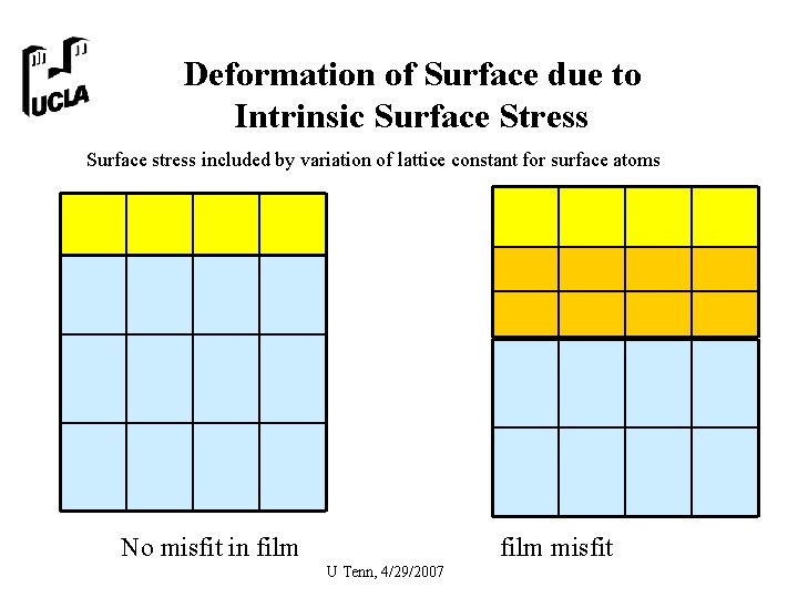
Deformation of Surface due to Intrinsic Surface Stress Surface stress included by variation of lattice constant for surface atoms No misfit in film misfit U Tenn, 4/29/2007

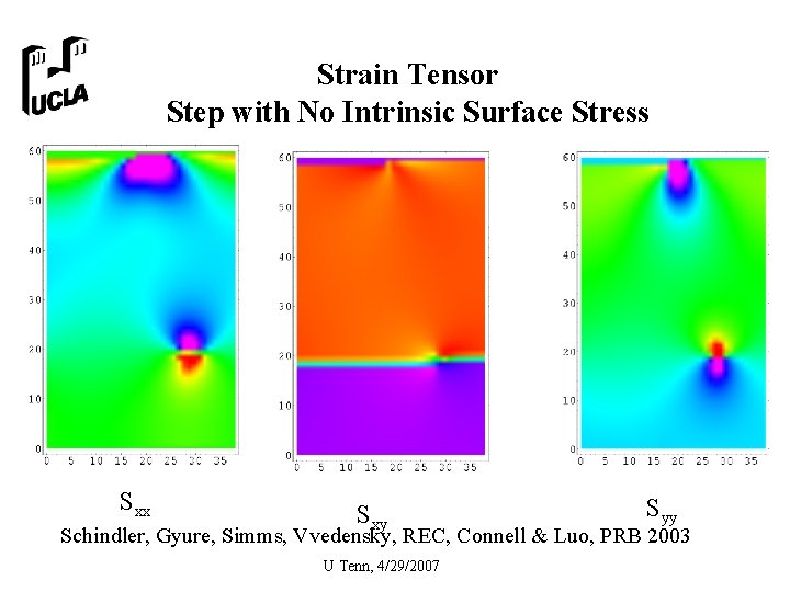
Strain Tensor Step with No Intrinsic Surface Stress Sxx Sxy Syy Schindler, Gyure, Simms, Vvedensky, REC, Connell & Luo, PRB 2003 U Tenn, 4/29/2007

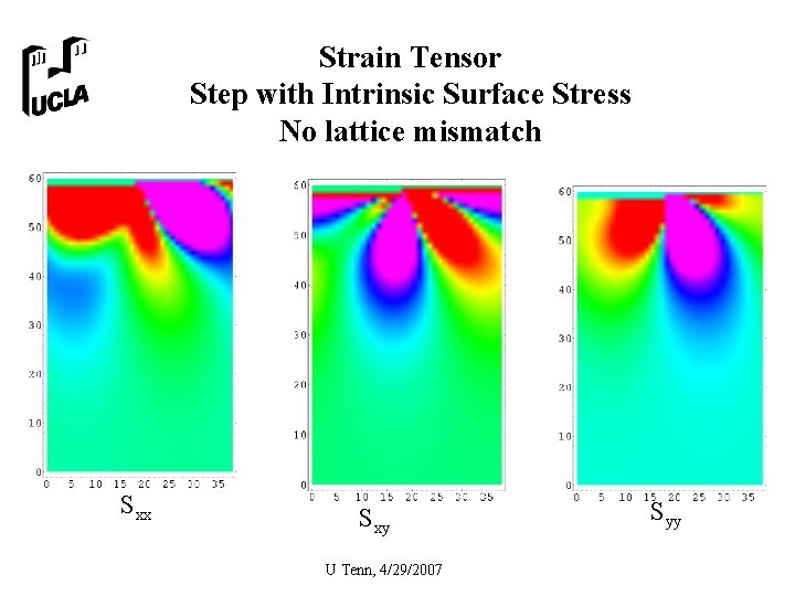
Strain Tensor Step with Intrinsic Surface Stress No lattice mismatch Sxx Sxy U Tenn, 4/29/2007 Syy

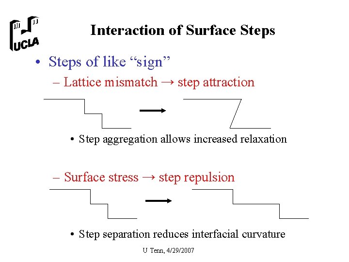
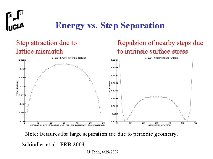
Interaction of Surface Steps • Steps of like “sign” – Lattice mismatch → step attraction • Step aggregation allows increased relaxation – Surface stress → step repulsion • Step separation reduces interfacial curvature U Tenn, 4/29/2007

Energy vs. Step Separation Step attraction due to lattice mismatch Repulsion of nearby steps due to intrinsic surface stress Note: Features for large separation are due to periodic geometry. Schindler et al. PRB 2003 U Tenn, 4/29/2007

Outline • Strain in epitaxial systems – Leads to structure – Quantum dots and their arrays • Atomistic strain model – Lattice statics model – Lattice mismatch • Numerical methods – Algebraic multigrid (AMG) – Artificial boundary conditions (ABC) • Application to nanowires – Step bunching instability • Summary U Tenn, 4/29/2007

Numerical method for Discrete Strain Equations • Algebraic multigrid with PCG • Artificial boundary conditions at top of substrate – Exact for discrete equations • 2 D and 3 D, MG and ABC combined – Russo & Smereka (JCP 2006), – Lee, REC & Lee (SIAP 2006) – REC, Lee, Shu Xiao, Xu (JCP 2006) U Tenn, 4/29/2007

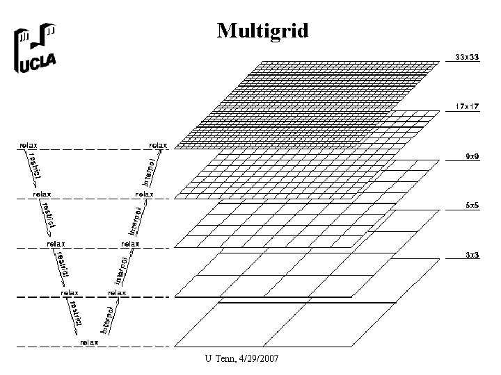
Multigrid • Solution performed on grids of different resolution – Average (fine grid) → coarse grid – Interpolate(coarse grid) → fine grid – Interaction between grids accelerates communication across the grid and convergence • (Geometric) multigrid (MG) – Averaging is performed over geometric neighbors • Algebraic multigrid (AMG) – Sparse matrix elements define a graph – Average is performed over adjacent points on graph U Tenn, 4/29/2007

Multigrid U Tenn, 4/29/2007

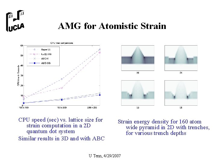
AMG for Atomistic Strain CPU speed (sec) vs. lattice size for strain computation in a 2 D quantum dot system Similar results in 3 D and with ABC Strain energy density for 160 atom wide pyramid in 2 D with trenches, for various trench depths U Tenn, 4/29/2007

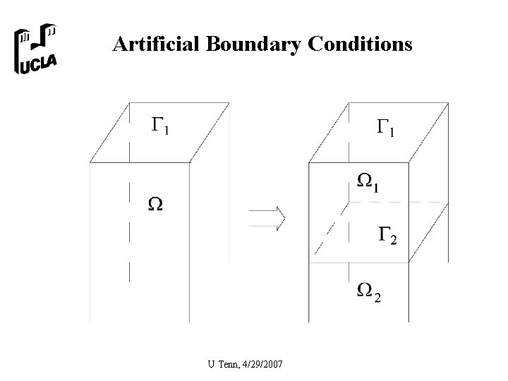
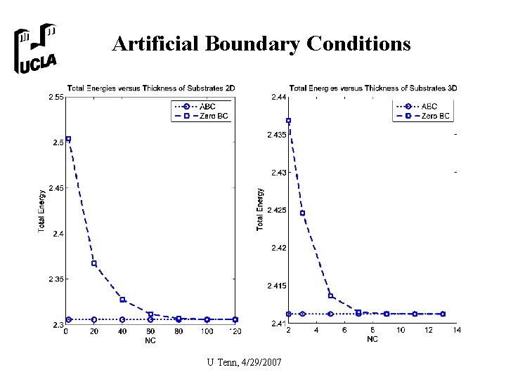
Artificial Boundary Conditions • For heteroepitaxial system, forces occur only at substrate/film interface – Below the interface, homogeneous elasticity – Exact solution in terms of Fourier transform • Reduction of solution domain – – – Γ = plane below interface Ω 1 = region above Γ, Ω 2 = region above Γ Exact artificial bdry condition (ABC) on Γ Solution only required on Ω 1, using ABC on Γ Formula for energy of entire system ( Ω 1 + Ω 2 ) • Exact ABCs developed for continuous and discrete systems U Tenn, 4/29/2007

Artificial Boundary Conditions U Tenn, 4/29/2007

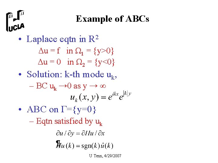
Example of ABCs • Laplace eqtn in R 2 Δu = f in Ω 1 = {y>0} Δu = 0 in Ω 2 = {y<0} • Solution: k-th mode uk, – BC uk → 0 as y → ∞ • ABC on Γ={y=0} – Eqtn satisfied by uk U Tenn, 4/29/2007

Artificial Boundary Conditions U Tenn, 4/29/2007

Outline • Strain in epitaxial systems – Leads to structure – Quantum dots and their arrays • Atomistic strain model – Lattice statics model – Lattice mismatch • Numerical methods – Algebraic multigrid (AMG) – Artificial boundary conditions (ABC) • Application to nanowires – Step bunching instability • Summary U Tenn, 4/29/2007

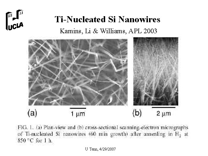
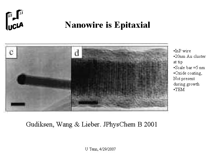
Nanowires • • Growth catalyzed by metal cluster (Au, Ti, …) Epitaxial Application to nano-electronics Stability difficulties U Tenn, 4/29/2007

Ti-Nucleated Si Nanowires Kamins, Li & Williams, APL 2003 U Tenn, 4/29/2007

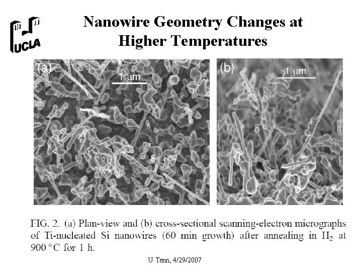
Nanowire Geometry Changes at Higher Temperatures U Tenn, 4/29/2007

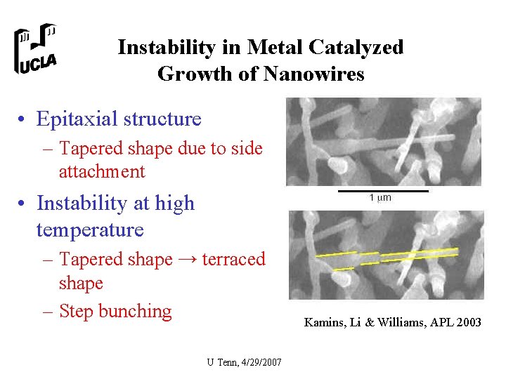
Instability in Metal Catalyzed Growth of Nanowires • Epitaxial structure – Tapered shape due to side attachment • Instability at high temperature – Tapered shape → terraced shape – Step bunching U Tenn, 4/29/2007 Kamins, Li & Williams, APL 2003

Nanowire is Epitaxial • In. P wire • 20 nm Au cluster at tip • Scale bar =5 nm • Oxide coating, Not present during growth • TEM Gudiksen, Wang & Lieber. JPhys. Chem B 2001 U Tenn, 4/29/2007

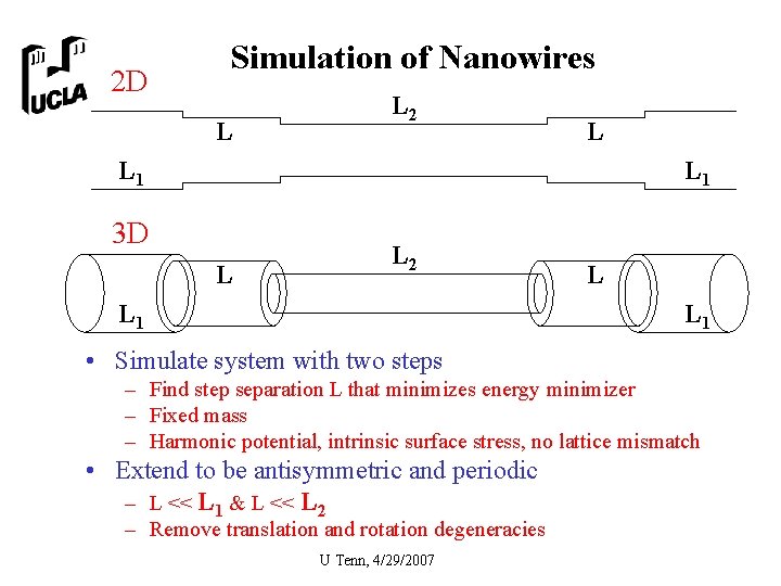
2 D Simulation of Nanowires L L 2 L L 1 3 D L L 2 L 1 L L 1 • Simulate system with two steps – Find step separation L that minimizes energy minimizer – Fixed mass – Harmonic potential, intrinsic surface stress, no lattice mismatch • Extend to be antisymmetric and periodic – L << L 1 & L << L 2 – Remove translation and rotation degeneracies U Tenn, 4/29/2007

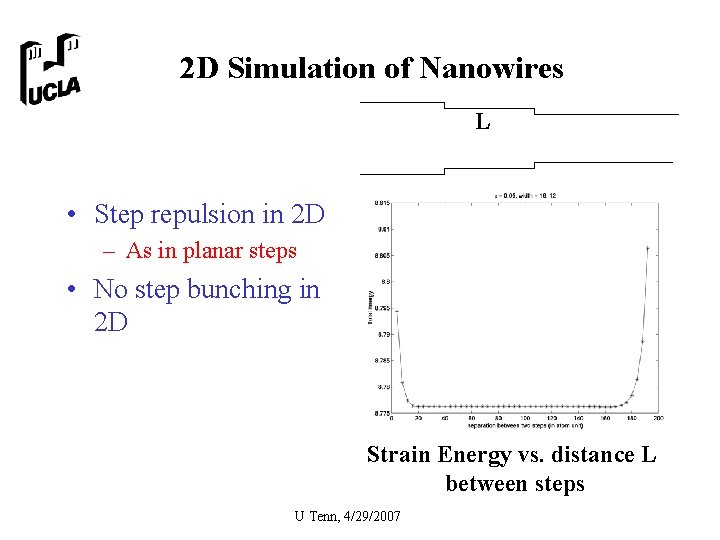
2 D Simulation of Nanowires L • Step repulsion in 2 D – As in planar steps • No step bunching in 2 D Strain Energy vs. distance L between steps U Tenn, 4/29/2007

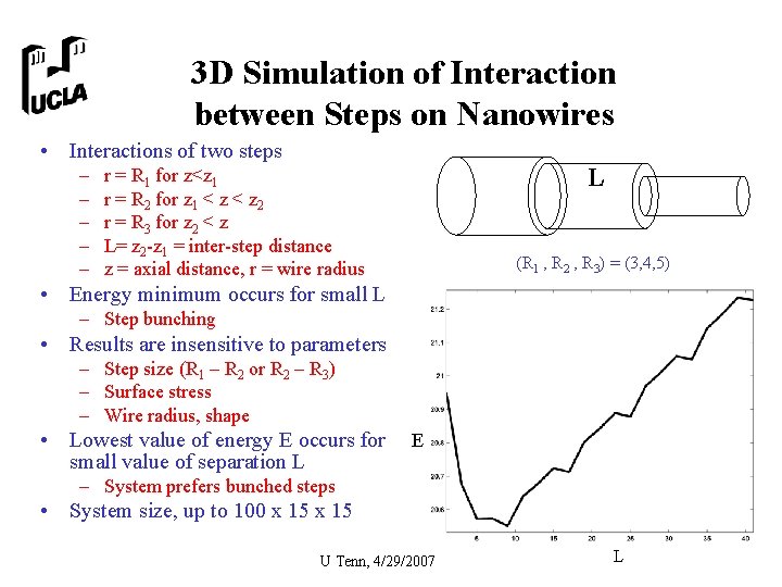
3 D Simulation of Interaction between Steps on Nanowires • Interactions of two steps – – – L r = R 1 for z<z 1 r = R 2 for z 1 < z 2 r = R 3 for z 2 < z L= z 2 -z 1 = inter-step distance z = axial distance, r = wire radius (R 1 , R 2 , R 3) = (3, 4, 5) • Energy minimum occurs for small L – Step bunching • Results are insensitive to parameters – Step size (R 1 – R 2 or R 2 – R 3) – Surface stress – Wire radius, shape • Lowest value of energy E occurs for small value of separation L E – System prefers bunched steps • System size, up to 100 x 15 U Tenn, 4/29/2007 L

Outline • Strain in epitaxial systems – Leads to structure – Quantum dots and their arrays • Atomistic strain model – Lattice statics model – Lattice mismatch • Numerical methods – Algebraic multigrid (AMG) – Artificial boundary conditions (ABC) • Application to nanowires – Step bunching instability • Summary U Tenn, 4/29/2007

Summary • Strain model – Harmonic potential – Minimal stencil – Surface stress represented by variation in lattice constant • Numerical methods – AMG – ABC • Nanowires – Surface stress – No step bunching in 2 D – Step bunching in 3 D U Tenn, 4/29/2007