Grazing incident Xray Diffraction XRD Xrays are electromagnetic
- Slides: 24

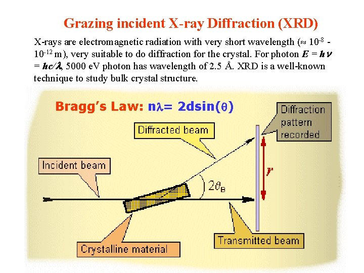
Grazing incident X-ray Diffraction (XRD) X-rays are electromagnetic radiation with very short wavelength ( 10 -8 10 -12 m), very suitable to do diffraction for the crystal. For photon E = hc/ , 5000 e. V photon has wavelength of 2. 5 Å. XRD is a well-known technique to study bulk crystal structure. Bragg’s Law: n = 2 dsin( )

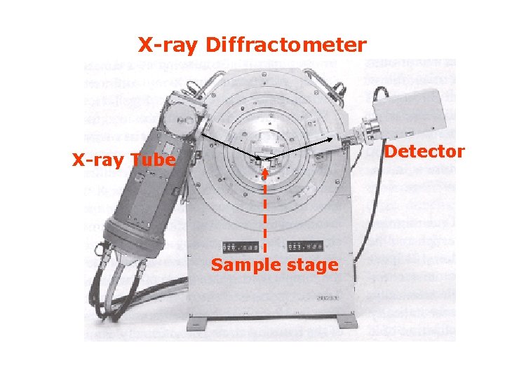
X-ray Diffractometer Detector X-ray Tube Sample stage

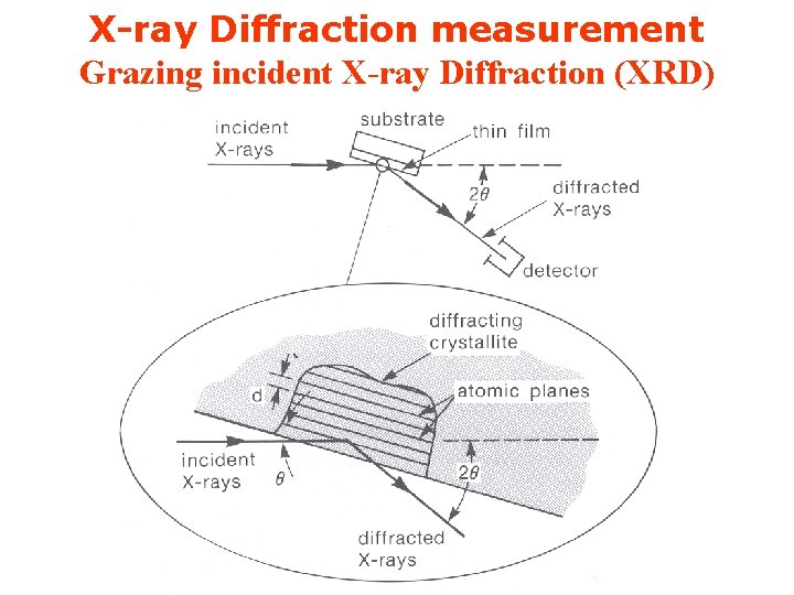
X-ray Diffraction measurement Grazing incident X-ray Diffraction (XRD)

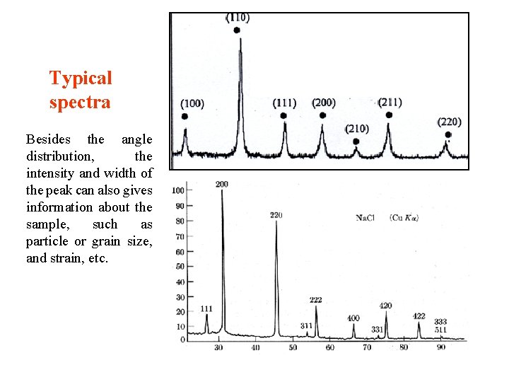
Typical spectra Besides the angle distribution, the intensity and width of the peak can also gives information about the sample, such as particle or grain size, and strain, etc.

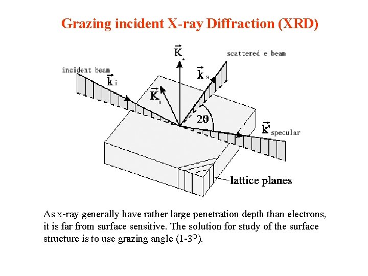
Grazing incident X-ray Diffraction (XRD) As x-ray generally have rather large penetration depth than electrons, it is far from surface sensitive. The solution for study of the surface structure is to use grazing angle (1 -3 O).

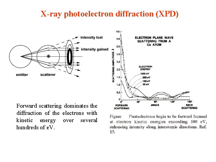
X-ray photoelectron diffraction (XPD) Forward scattering dominates the diffraction of the electrons with kinetic energy over several hundreds of e. V.

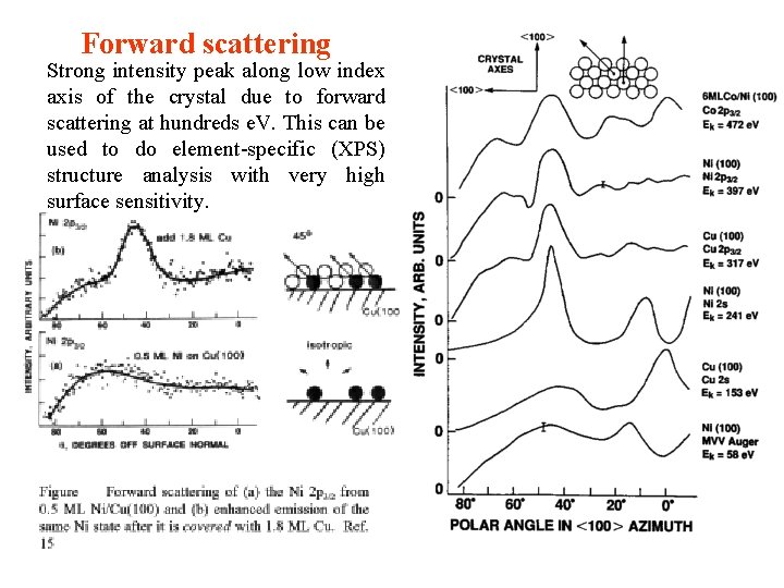
Forward scattering Strong intensity peak along low index axis of the crystal due to forward scattering at hundreds e. V. This can be used to do element-specific (XPS) structure analysis with very high surface sensitivity.

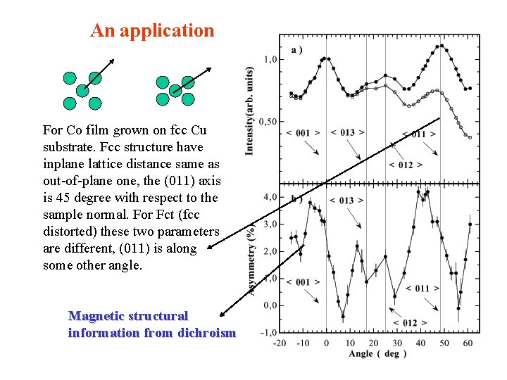
An application For Co film grown on fcc Cu substrate. Fcc structure have inplane lattice distance same as out-of-plane one, the (011) axis is 45 degree with respect to the sample normal. For Fct (fcc distorted) these two parameters are different, (011) is along some other angle. Magnetic structural information from dichroism

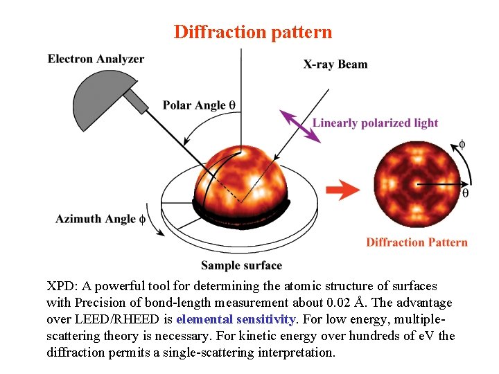
Diffraction pattern XPD: A powerful tool for determining the atomic structure of surfaces with Precision of bond-length measurement about 0. 02 Å. The advantage over LEED/RHEED is elemental sensitivity. For low energy, multiplescattering theory is necessary. For kinetic energy over hundreds of e. V the diffraction permits a single-scattering interpretation.

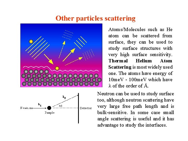
Other particles scattering Atoms/Molecules such as He atom can be scattered from surface, they can be used to study surface structures with very high surface sensitivity. Thermal Helium Atom Scattering is most widely used one. The atoms have energy of 10 me. V - 100 me. V which have l of the order of Å. Neutron can be used to study surface too, although neutron scattering have very large free path length and is bulk-sensitive. In some case small angle scattering is useful and it has advantage to study the interfaces.

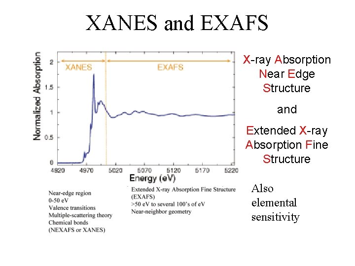
XANES and EXAFS X-ray Absorption Near Edge Structure and Extended X-ray Absorption Fine Structure Also elemental sensitivity

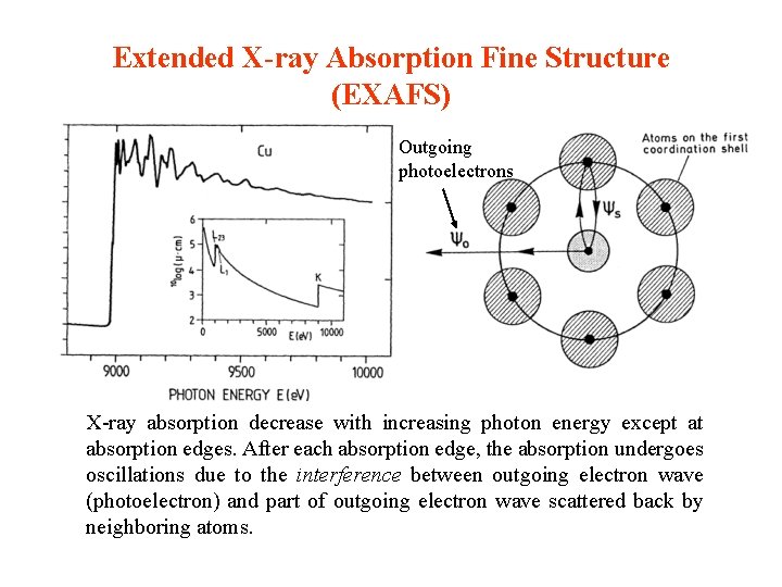
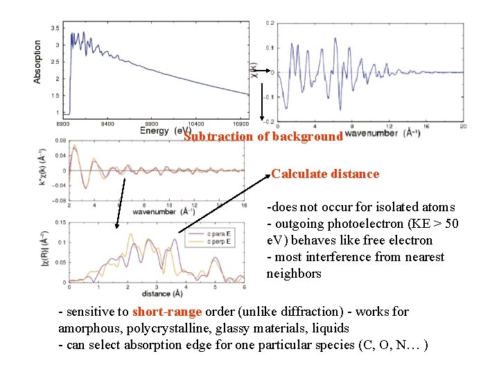
Extended X-ray Absorption Fine Structure (EXAFS) Outgoing photoelectrons X-ray absorption decrease with increasing photon energy except at absorption edges. After each absorption edge, the absorption undergoes oscillations due to the interference between outgoing electron wave (photoelectron) and part of outgoing electron wave scattered back by neighboring atoms.

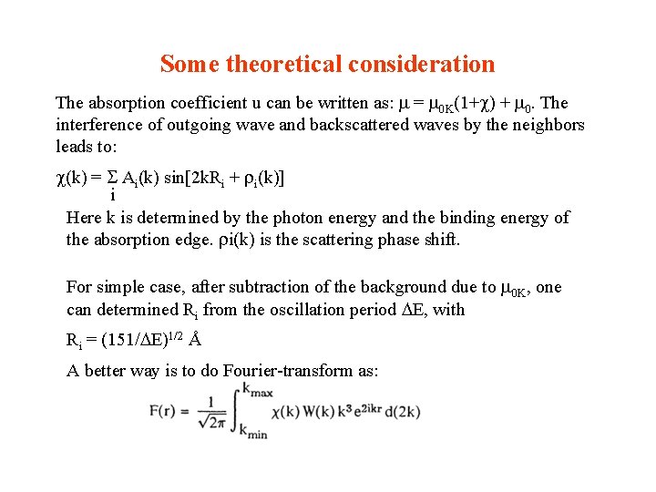
Some theoretical consideration The absorption coefficient u can be written as: m = m 0 K(1+c) + m 0. The interference of outgoing wave and backscattered waves by the neighbors leads to: c(k) = S Ai(k) sin[2 k. Ri + ri(k)] i Here k is determined by the photon energy and the binding energy of the absorption edge. ri(k) is the scattering phase shift. For simple case, after subtraction of the background due to m 0 K, one can determined Ri from the oscillation period DE, with Ri = (151/DE)1/2 Å A better way is to do Fourier-transform as:

Subtraction of background Calculate distance -does not occur for isolated atoms - outgoing photoelectron (KE > 50 e. V) behaves like free electron - most interference from nearest neighbors - sensitive to short-range order (unlike diffraction) - works for amorphous, polycrystalline, glassy materials, liquids - can select absorption edge for one particular species (C, O, N… )

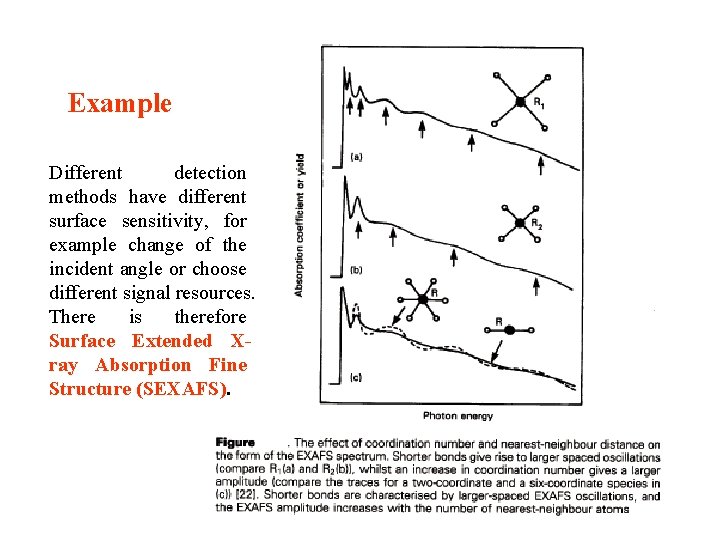
Example Different detection methods have different surface sensitivity, for example change of the incident angle or choose different signal resources. There is therefore Surface Extended Xray Absorption Fine Structure (SEXAFS).

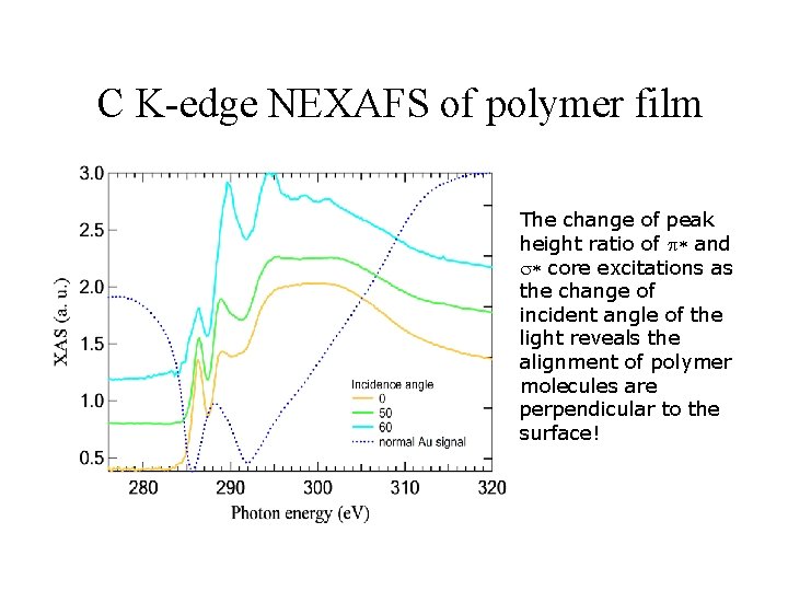
C K-edge NEXAFS of polymer film The change of peak height ratio of p* and s* core excitations as the change of incident angle of the light reveals the alignment of polymer molecules are perpendicular to the surface!

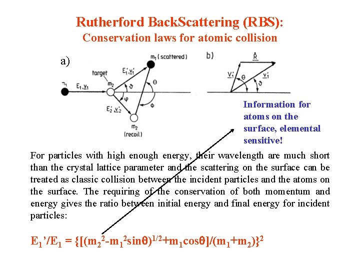
Rutherford Back. Scattering (RBS): Conservation laws for atomic collision a) Information for atoms on the surface, elemental sensitive! For particles with high enough energy, their wavelength are much short than the crystal lattice parameter and the scattering on the surface can be treated as classic collision between the incident particles and the atoms on the surface. The requiring of the conservation of both momentum and energy gives the ratio between initial energy and final energy for incident particles: E 1’/E 1 = {[(m 22 -m 12 sin )1/2+m 1 cos ]/(m 1+m 2)}2

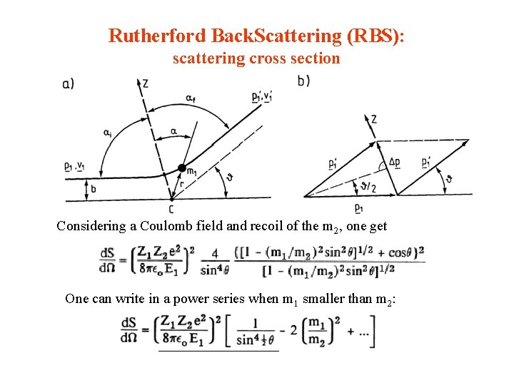
Rutherford Back. Scattering (RBS): scattering cross section Considering a Coulomb field and recoil of the m 2, one get One can write in a power series when m 1 smaller than m 2:

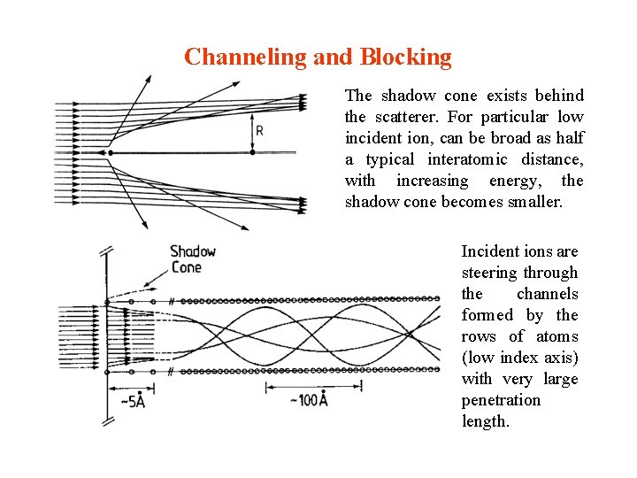
Channeling and Blocking The shadow cone exists behind the scatterer. For particular low incident ion, can be broad as half a typical interatomic distance, with increasing energy, the shadow cone becomes smaller. Incident ions are steering through the channels formed by the rows of atoms (low index axis) with very large penetration length.

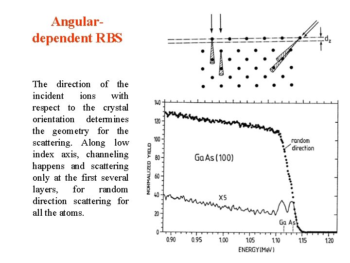
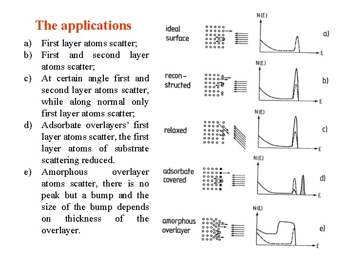
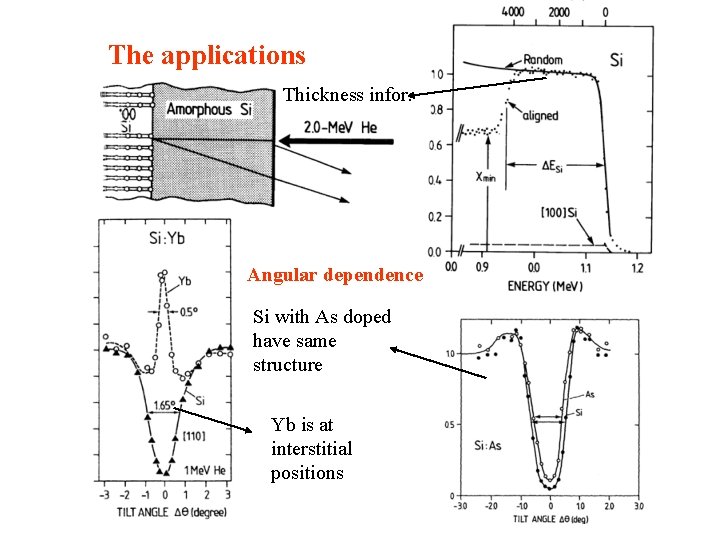
Angulardependent RBS The direction of the incident ions with respect to the crystal orientation determines the geometry for the scattering. Along low index axis, channeling happens and scattering only at the first several layers, for random direction scattering for all the atoms.

The applications a) First layer atoms scatter; b) First and second layer atoms scatter; c) At certain angle first and second layer atoms scatter, while along normal only first layer atoms scatter; d) Adsorbate overlayers’ first layer atoms scatter, the first layer atoms of substrate scattering reduced. e) Amorphous overlayer atoms scatter, there is no peak but a bump and the size of the bump depends on thickness of the overlayer.

The applications Thickness infor. Angular dependence Si with As doped have same structure Yb is at interstitial positions

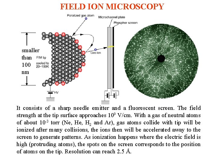
FIELD ION MICROSCOPY smaller than 100 nm It consists of a sharp needle emitter and a fluorescent screen. The field strength at the tip surface approaches 109 V/cm. With a gas of neutral atoms of about 10 -3 torr (Ne, H 2 and Ar), gas atoms collide with tip will be ionized after many collisions, the ions then will be accelerated away to the screen to generate patterns. As ionization happens where the electric field is high (protruding atoms), the spots on the screen corresponds to the position of atoms on the tip. Resolution can reach 2. 5 Å.

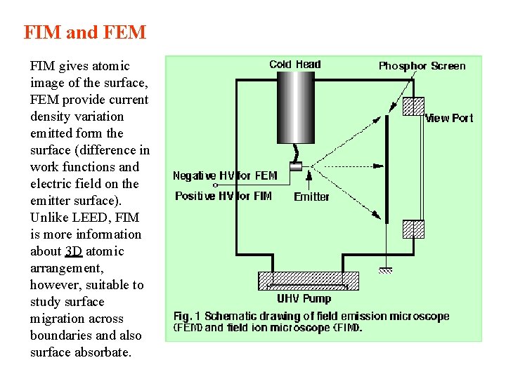
FIM and FEM FIM gives atomic image of the surface, FEM provide current density variation emitted form the surface (difference in work functions and electric field on the emitter surface). Unlike LEED, FIM is more information about 3 D atomic arrangement, however, suitable to study surface migration across boundaries and also surface absorbate.