Graphene CastroNeto et al Rev Mod Phys 81

- Slides: 30

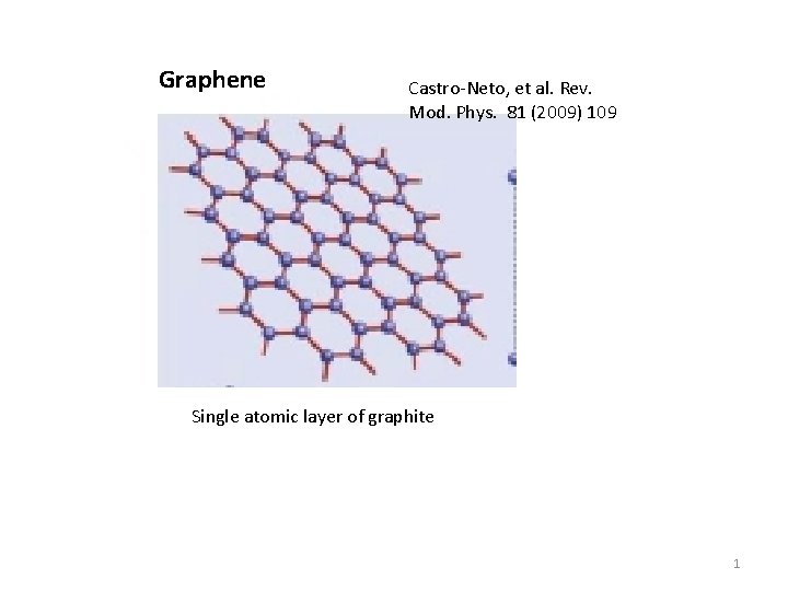
Graphene Castro-Neto, et al. Rev. Mod. Phys. 81 (2009) 109 Single atomic layer of graphite 1

I. Graphene Electronic Properties (isolated graphene sheets) II. Graphene Formation—Growth on Si. C III. Graphene Growth on BN, Co 3 O 4, etc. 2

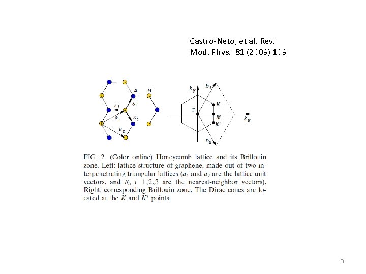
Castro-Neto, et al. Rev. Mod. Phys. 81 (2009) 109 3

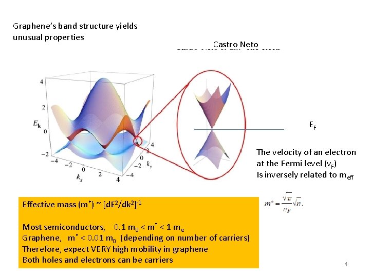
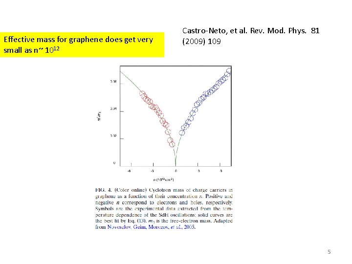
Graphene’s band structure yields unusual properties Castro Neto EF The velocity of an electron at the Fermi level (v. F) Is inversely related to meff Effective mass (m*) ~ [d. E 2/dk 2]-1 Most semiconductors, 0. 1 m 0 < m* < 1 me Graphene, m* < 0. 01 m 0 (depending on number of carriers) Therefore, expect VERY high mobility in graphene Both holes and electrons can be carriers 4

Effective mass for graphene does get very small as n~ 1012 Castro-Neto, et al. Rev. Mod. Phys. 81 (2009) 109 5

6

The Big Problem with graphene: an imagined conversation: A. OK: Graphene is great, lots of interesting properties for devices! B. How do you make a device? A. You need a sheet of graphene! B. OK, how do you get a sheet of graphene? A. HOPG, scotch tape, and tweezers! B. !@#$%% 7

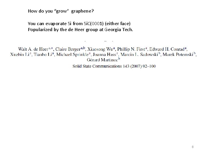
How do you “grow” graphene? You can evaporate Si from Si. C(0001) (either face) Popularized by the de Heer group at Georgia Tech. 8

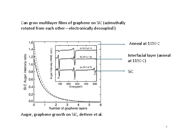
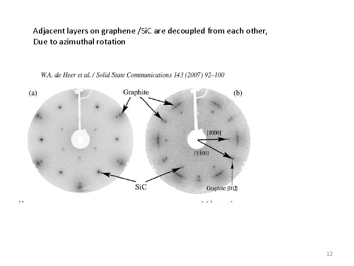
Can grow multilayer films of graphene on Si. C (azimuthally rotated from each other—electronically decoupled!) Anneal at 1350 C Interfacial layer (anneal at 1150 C) Si. C Auger, graphene growth on Si. C, de. Heer et al. 9

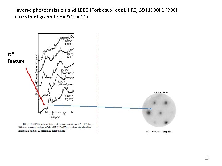
Inverse photoemission and LEED (Forbeaux, et al, PRB, 58 (1998) 16396) Growth of graphite on Si. C(0001) π* feature 10

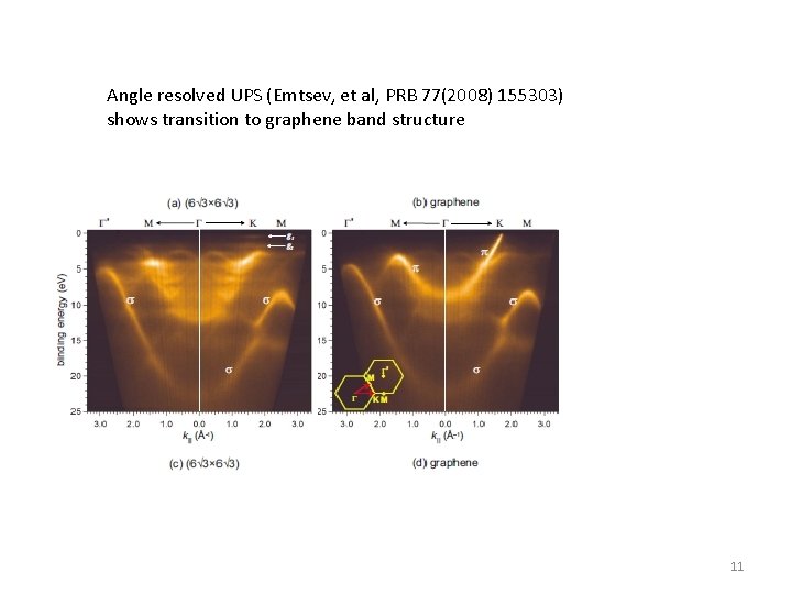
Angle resolved UPS (Emtsev, et al, PRB 77(2008) 155303) shows transition to graphene band structure 11

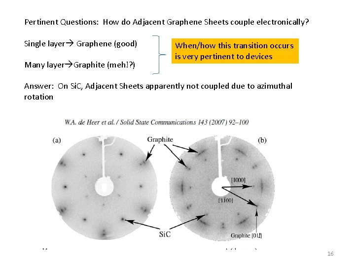
Adjacent layers on graphene /Si. C are decoupled from each other, Due to azimuthal rotation 12

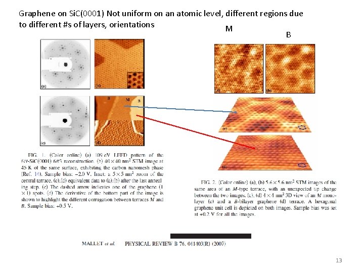
Graphene on Si. C(0001) Not uniform on an atomic level, different regions due to different #s of layers, orientations M B 13

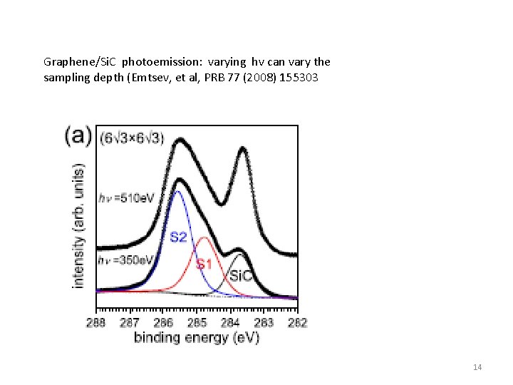
Graphene/Si. C photoemission: varying hv can vary the sampling depth (Emtsev, et al, PRB 77 (2008) 155303 14

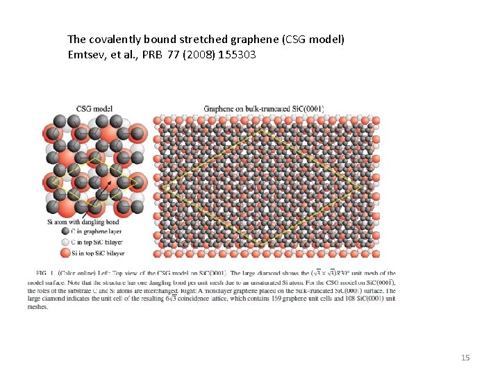
The covalently bound stretched graphene (CSG model) Emtsev, et al. , PRB 77 (2008) 155303 15

Pertinent Questions: How do Adjacent Graphene Sheets couple electronically? Single layer Graphene (good) Many layer Graphite (meh!? ) When/how this transition occurs is very pertinent to devices Answer: On Si. C, Adjacent Sheets apparently not coupled due to azimuthal rotation 16

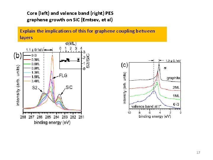
Core (left) and valence band (right) PES graphene growth on Si. C (Emtsev, et al) Explain the implications of this for graphene coupling between layers 17

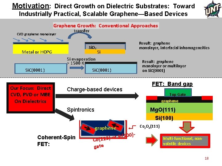
Motivation: Direct Growth on Dielectric Substrates: Toward Industrially Practical, Scalable Graphene—Based Devices Graphene Growth: Conventional Approaches CVD graphene monolayer transfer Si. O 2 Metal or HOPG Si. C(0001) Our Focus: Direct CVD, PVD or MBE On Dielectrics Result: graphene monolayer, interfacial inhomogeneities Si Si evaporation > 1500 K Si. C(0001) Result: graphene monolayer or multilayer on Si. C(0001) FET: Band gap Charge-based devices n Spintronics graphene Mg. O(111) Si(100) Co 3 O 4(111) graphene Coherent-Spin FET: Top Gate 00)- r Si(1 o ) 1 1 1 ( o C gate Multi-functional, nonvolatile devices 18

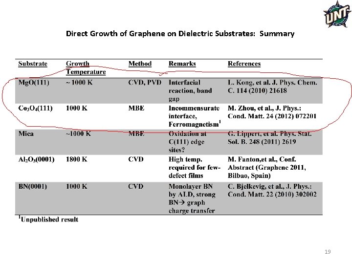
Direct Growth of Graphene on Dielectric Substrates: Summary 19

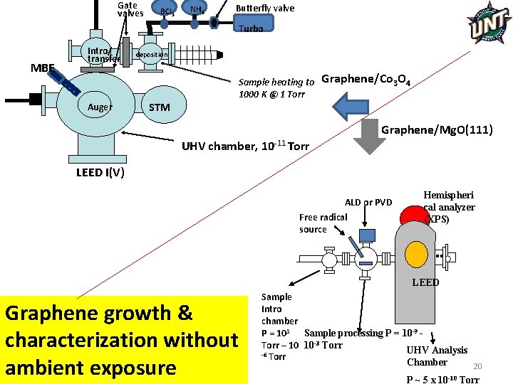
Gate valves BCl 3 NH 3 Butterfly valve Turbo MBE Intro/ transfer deposition Sample heating to 1000 K @ 1 Torr Auger Graphene/Co 3 O 4 STM Graphene/Mg. O(111) UHV chamber, 10 -11 Torr LEED I(V) ALD or PVD Free radical source Hemispheri cal analyzer (XPS) LEED Graphene growth & characterization without ambient exposure Sample Intro chamber P = 103 Sample processing P = 10 -9 Torr – 10 10 -3 Torr UHV Analysis -6 Torr Chamber 20 P ~ 5 x 10 -10 Torr

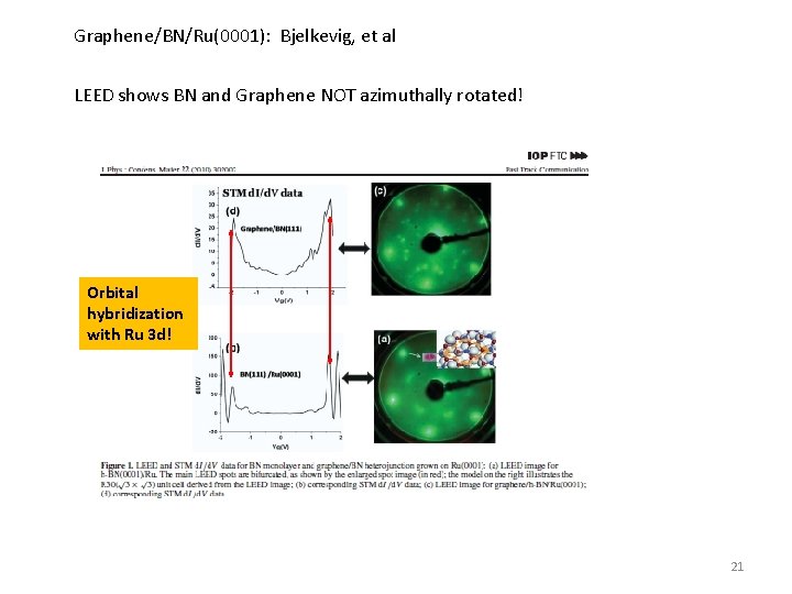
Graphene/BN/Ru(0001): Bjelkevig, et al LEED shows BN and Graphene NOT azimuthally rotated! Orbital hybridization with Ru 3 d! 21

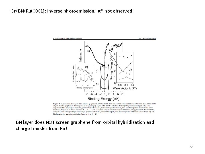
Gr/BN/Ru(0001): Inverse photoemission. π* not observed! BN layer does NOT screen graphene from orbital hybridization and charge transfer from Ru! 22

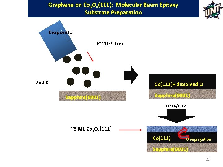
Graphene on Co 3 O 4(111): Molecular Beam Epitaxy Substrate Preparation Evaporator P~ 10 -8 Torr 750 K Co(111)+ dissolved O Sapphire(0001) 1000 K/UHV ~3 ML Co 3 O 4(111) Co(111) O segregation Sapphire(0001) 23

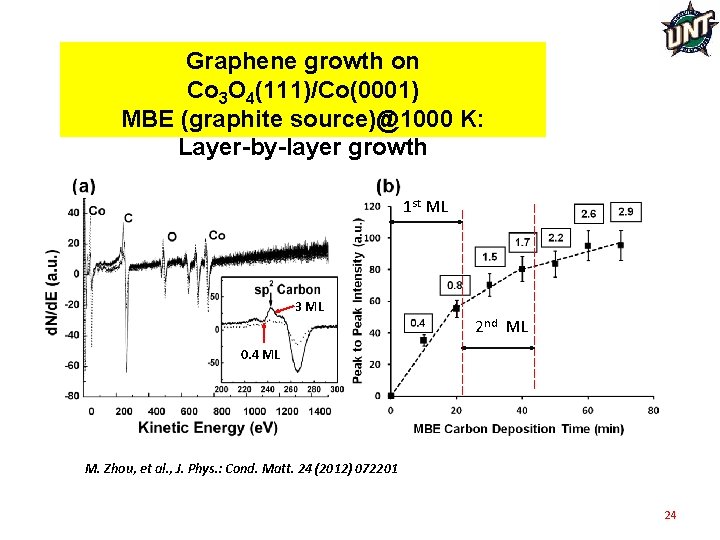
Graphene growth on Co 3 O 4(111)/Co(0001) MBE (graphite source)@1000 K: Layer-by-layer growth 1 st ML 3 ML 2 nd ML 0. 4 ML M. Zhou, et al. , J. Phys. : Cond. Matt. 24 (2012) 072201 24

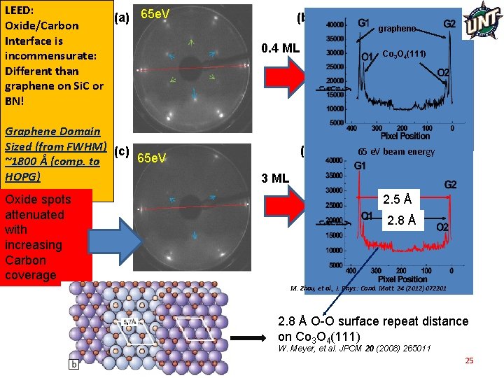
LEED: (a) 65 e. V Oxide/Carbon Interface is incommensurate: Different than graphene on Si. C or BN! Graphene Domain Sized (from FWHM) (c) 65 e. V ~1800 Å (comp. to HOPG) Oxide spots attenuated with increasing Carbon coverage (b) 0. 4 ML (d) graphene Co 3 O 4(111) 65 e. V beam energy 3 ML 2. 5 Å 2. 8 Å M. Zhou, et al. , J. Phys. : Cond. Matt. 24 (2012) 072201 2. 8 Å O-O surface repeat distance on Co 3 O 4(111) W. Meyer, et al. JPCM 20 (2008) 265011 25

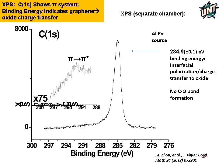
XPS: C(1 s) Shows π system: Binding Energy indicates graphene oxide charge transfer XPS (separate chamber): Al Kα source π→π* 284. 9(± 0. 1) e. V binding energy: Interfacial polarization/charge transfer to oxide No C-O bond formation M. Zhou, et al. , J. Phys. : Cond. 26 Matt. 24 (2012) 072201

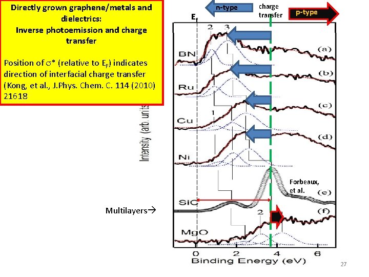
Directly grown graphene/metals and dielectrics: Inverse photoemission and charge transfer Ef n-type charge transfer p-type Position of * (relative to EF) indicates direction of interfacial charge transfer (Kong, et al. , J. Phys. Chem. C. 114 (2010) 21618 Forbeaux, et al. Multilayers 27

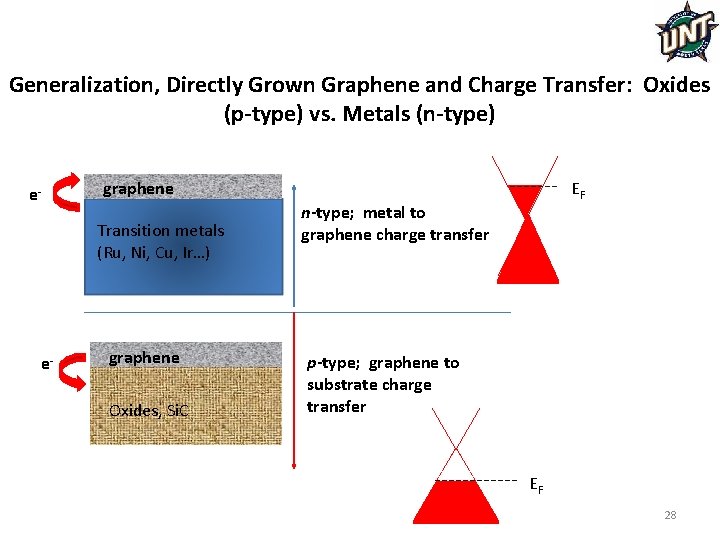
Generalization, Directly Grown Graphene and Charge Transfer: Oxides (p-type) vs. Metals (n-type) e- graphene Transition metals (Ru, Ni, Cu, Ir…) e- graphene Oxides, Si. C EF n-type; metal to graphene charge transfer p-type; graphene to substrate charge transfer EF 28

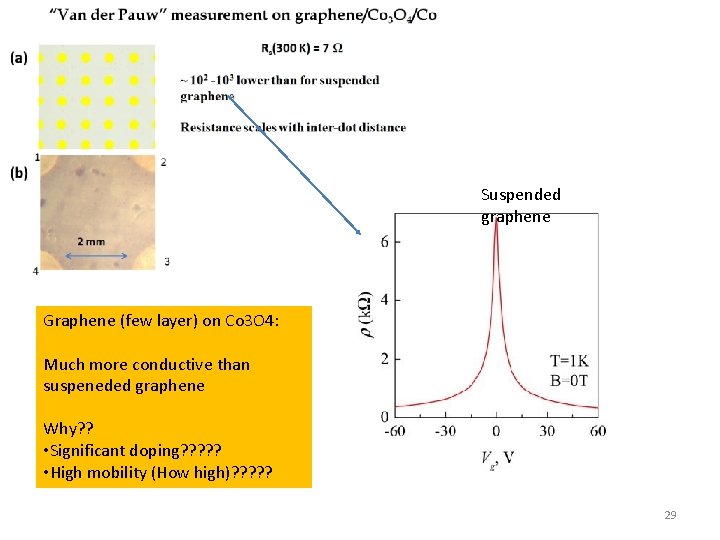
Suspended graphene Graphene (few layer) on Co 3 O 4: Much more conductive than suspeneded graphene Why? ? • Significant doping? ? ? • High mobility (How high)? ? ? 29

Conclusion: Graphene: Large area growth on practical substrates critical for device development. Interactions with substrates and (maybe) other graphene layers are critical to device properties 30