
GRAPHENE Anita Kulkarni May 8 2018 1 Outline
- Slides: 25
GRAPHENE Anita Kulkarni May 8, 2018 1
Outline • Introduction • Chemistry and physics of graphene • Emphasis on electrical properties • Connections to disparate areas of physics • Some potential applications… • And this does not even scratch the surface! 2
Unlocking the Door to 2 D Materials • Subject of 2010 Nobel Prize in Physics • Isolated by Andre K. Geim and Konstantin Novoselov at the University of Manchester in 2004 • Isolated and experimentally characterized the first 2 D material ever when this was thought unfeasible due to thermodynamic instability • Discovery led to intense study of graphene and other 2 D materials 3
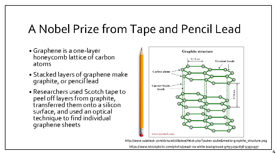
A Nobel Prize from Tape and Pencil Lead • Graphene is a one-layer honeycomb lattice of carbon atoms • Stacked layers of graphene make graphite, or pencil lead • Researchers used Scotch tape to peel off layers from graphite, transferred them onto a silicon surface, and used an optical technique to find individual graphene sheets http: //www. substech. com/dokuwiki/lib/exe/fetch. php? cache=cache&media=graphite_structure. png https: //www. istockphoto. com/photo/pencil-on-white-background-gm 531792638 -93951957 4
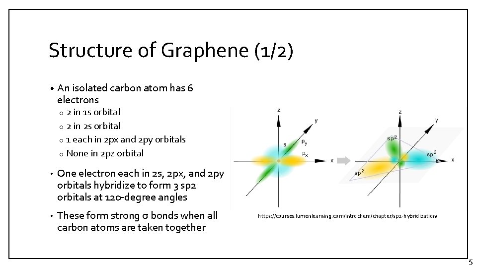
Structure of Graphene (1/2) • An isolated carbon atom has 6 electrons o 2 in 1 s orbital o 2 in 2 s orbital o 1 each in 2 px and 2 py orbitals o None in 2 pz orbital • One electron each in 2 s, 2 px, and 2 py orbitals hybridize to form 3 sp 2 orbitals at 120 -degree angles • These form strong σ bonds when all carbon atoms are taken together https: //courses. lumenlearning. com/introchem/chapter/sp 2 -hybridization/ 5
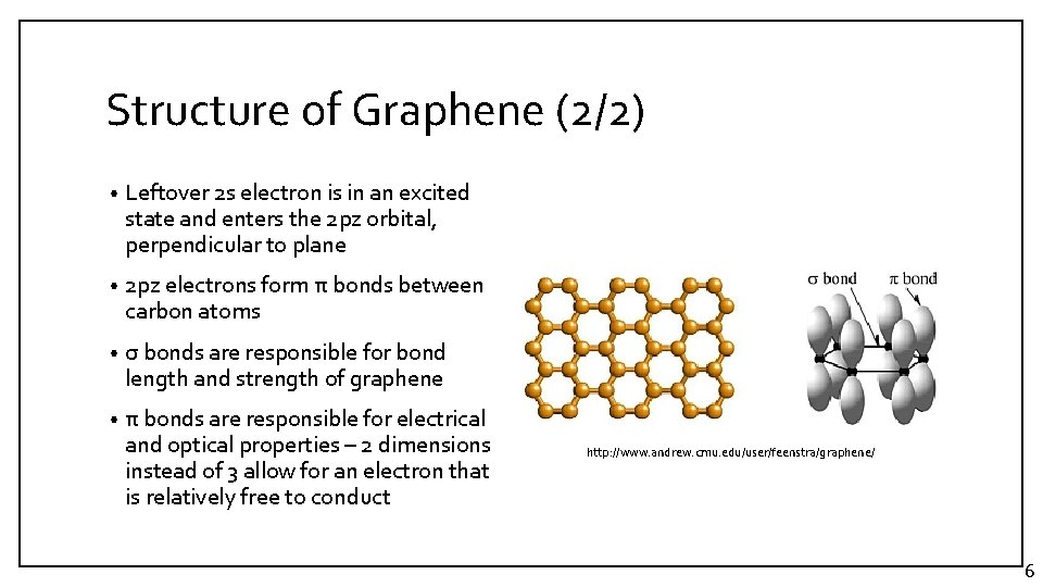
Structure of Graphene (2/2) • Leftover 2 s electron is in an excited state and enters the 2 pz orbital, perpendicular to plane • 2 pz electrons form π bonds between carbon atoms • σ bonds are responsible for bond length and strength of graphene • π bonds are responsible for electrical and optical properties – 2 dimensions instead of 3 allow for an electron that is relatively free to conduct http: //www. andrew. cmu. edu/user/feenstra/graphene/ 6
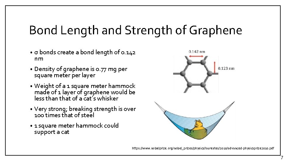
Bond Length and Strength of Graphene • σ bonds create a bond length of 0. 142 nm • Density of graphene is 0. 77 mg per square meter per layer • Weight of a 1 square meter hammock made of 1 layer of graphene would be less than that of a cat’s whisker • Very strong; breaking strength is over 100 times that of steel • 1 square meter hammock could support a cat https: //www. nobelprize. org/nobel_prizes/physics/laureates/2010/advanced-physicsprize 2010. pdf 7
Deriving Electronic Properties: Necessity of a Quantum Mechanical Model • To predict electronic properties, a quantum mechanical model is needed • First, find a way to represent the “potential energy landscape” (the potential energy at each point in space) the electrons see in the material • This landscape is made up of: o Attraction to the positively charged nuclei o Repulsion from the other negatively charged electrons • Solve the Schrödinger equation (central to quantum mechanics) with this energy landscape to derive electronic properties 8
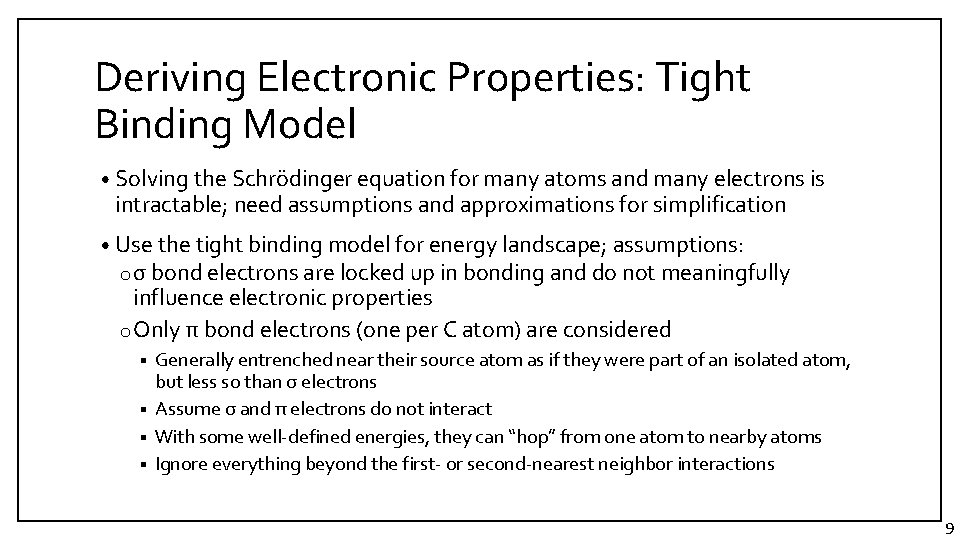
Deriving Electronic Properties: Tight Binding Model • Solving the Schrödinger equation for many atoms and many electrons is intractable; need assumptions and approximations for simplification • Use the tight binding model for energy landscape; assumptions: o σ bond electrons are locked up in bonding and do not meaningfully influence electronic properties o Only π bond electrons (one per C atom) are considered Generally entrenched near their source atom as if they were part of an isolated atom, but less so than σ electrons § Assume σ and π electrons do not interact § With some well-defined energies, they can “hop” from one atom to nearby atoms § Ignore everything beyond the first- or second-nearest neighbor interactions § 9
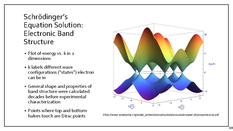
Schrödinger’s Equation Solution: Electronic Band Structure • Plot of energy vs. k in 2 dimensions • k labels different wave configurations (“states”) electron can be in • General shape and properties of band structure were calculated decades before experimental characterization • Points where top and bottom halves touch are Dirac points https: //www. nobelprize. org/nobel_prizes/physics/laureates/2010/advanced-physicsprize 2010. pdf 10
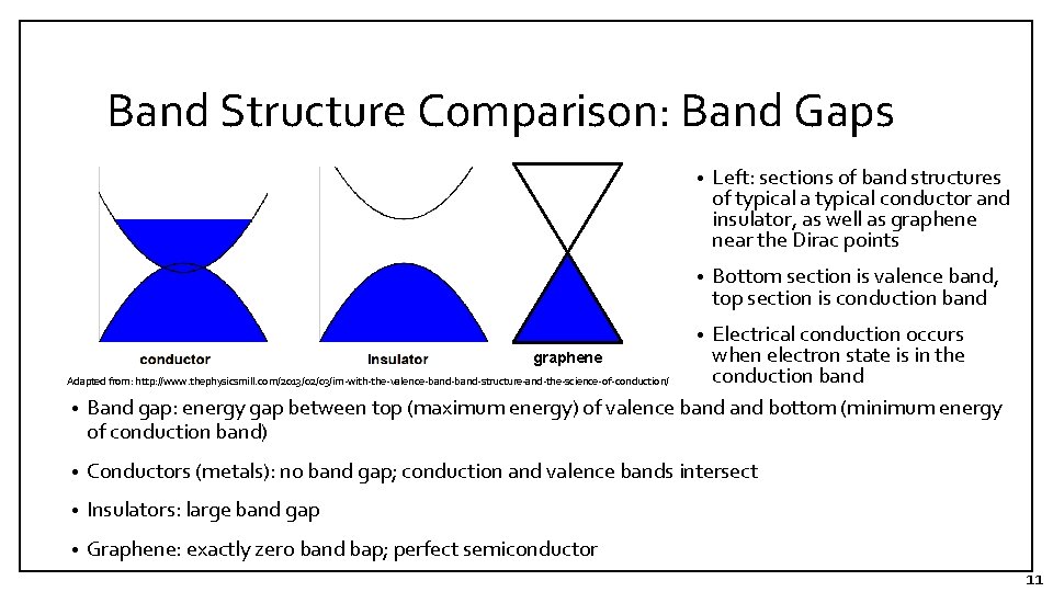
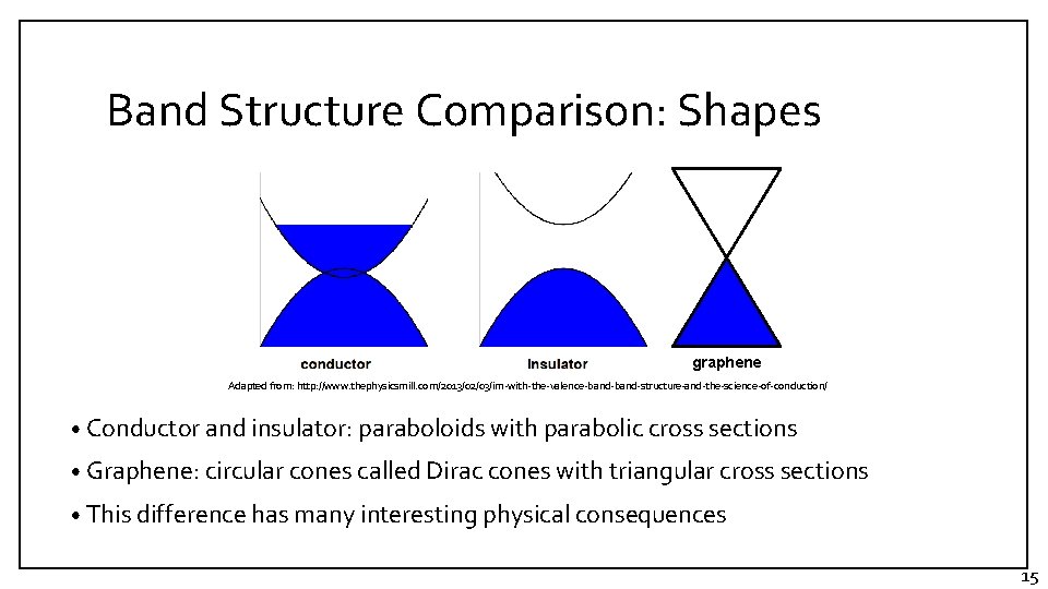
Band Structure Comparison: Band Gaps • Left: sections of band structures of typical a typical conductor and insulator, as well as graphene near the Dirac points • Bottom section is valence band, top section is conduction band Electrical conduction occurs when electron state is in the graphene conduction band Adapted from: http: //www. thephysicsmill. com/2013/02/03/im-with-the-valence-band-structure-and-the-science-of-conduction/ • Band gap: energy gap between top (maximum energy) of valence band bottom (minimum energy of conduction band) • • Conductors (metals): no band gap; conduction and valence bands intersect • Insulators: large band gap • Graphene: exactly zero band bap; perfect semiconductor 11
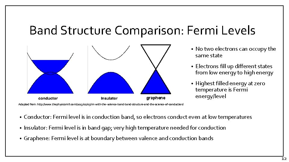
Band Structure Comparison: Fermi Levels graphene • No two electrons can occupy the same state • Electrons fill up different states from low energy to high energy • Highest filled energy at zero temperature is Fermi energy/level Adapted from: http: //www. thephysicsmill. com/2013/02/03/im-with-the-valence-band-structure-and-the-science-of-conduction/ • Conductor: Fermi level is in conduction band, so electrons conduct even at low temperatures • Insulator: Fermi level is in band gap; very high temperature needed for conduction • Graphene: Fermi level is at boundary between valence and conduction bands 12
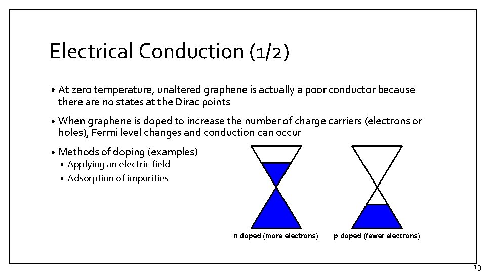
Electrical Conduction (1/2) • At zero temperature, unaltered graphene is actually a poor conductor because there are no states at the Dirac points • When graphene is doped to increase the number of charge carriers (electrons or holes), Fermi level changes and conduction can occur • Methods of doping (examples) Applying an electric field • Adsorption of impurities • n doped (more electrons) p doped (fewer electrons) 13
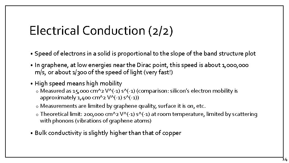
Electrical Conduction (2/2) • Speed of electrons in a solid is proportional to the slope of the band structure plot • In graphene, at low energies near the Dirac point, this speed is about 1, 000 m/s, or about 1/300 of the speed of light (very fast!) • High speed means high mobility o Measured as 15, 000 cm^2 V^(-1) s^(-1) (comparison: silicon’s electron mobility is approximately 1, 400 cm^2 V^(-1) s^(-1)) o Measurements are limited by graphene quality, surface it is on, etc. o Theoretical limit: 200, 000 cm^2 V^(-1) s^(-1) at room temperature, limited by scattering with phonons (vibrations of graphene atoms) • Bulk conductivity is slightly higher than that of copper 14
Band Structure Comparison: Shapes graphene Adapted from: http: //www. thephysicsmill. com/2013/02/03/im-with-the-valence-band-structure-and-the-science-of-conduction/ • Conductor and insulator: paraboloids with parabolic cross sections • Graphene: circular cones called Dirac cones with triangular cross sections • This difference has many interesting physical consequences 15
A Laboratory for Quantum Electrodynamics (QED): Introduction • Dirac cone: linear instead of quadratic relationship between energy and k • Linearity means constant slope and constant speed with respect to k – just like a photon! • Equation for electron behavior has the same form as QED’s Dirac equation of massless fermions at a constant speed • Low-energy electrons can be studied to observe QED-type effects otherwise seen in particle physics 16
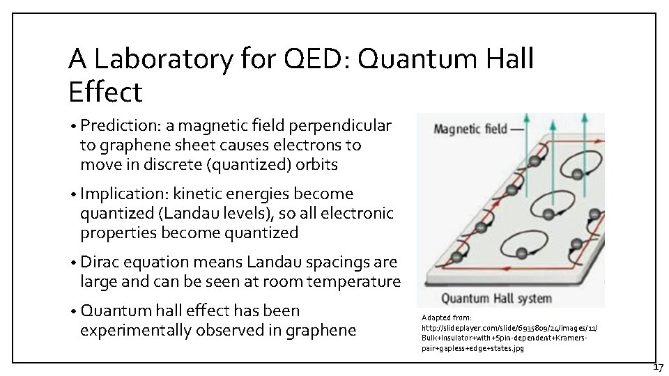
A Laboratory for QED: Quantum Hall Effect • Prediction: a magnetic field perpendicular to graphene sheet causes electrons to move in discrete (quantized) orbits • Implication: kinetic energies become quantized (Landau levels), so all electronic properties become quantized • Dirac equation means Landau spacings are large and can be seen at room temperature • Quantum hall effect has been experimentally observed in graphene Adapted from: http: //slideplayer. com/slide/6935809/24/images/11/ Bulk+Insulator+with+Spin-dependent+Kramerspair+gapless+edge+states. jpg 17
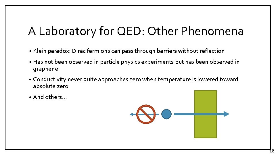
A Laboratory for QED: Other Phenomena • Klein paradox: Dirac fermions can pass through barriers without reflection • Has not been observed in particle physics experiments but has been observed in graphene • Conductivity never quite approaches zero when temperature is lowered toward absolute zero • And others… 18
A Sampling of Cutting-Edge Research • Physics of graphene is a very active subject of research • Increased scattering at increased temperatures causes electrons in graphene to behave like a viscous fluid and decrease resistance • Vibrating carbon atoms provide an ever-present voltage • Offset 2 -layer graphene may behave like a high-temperature superconductor 19
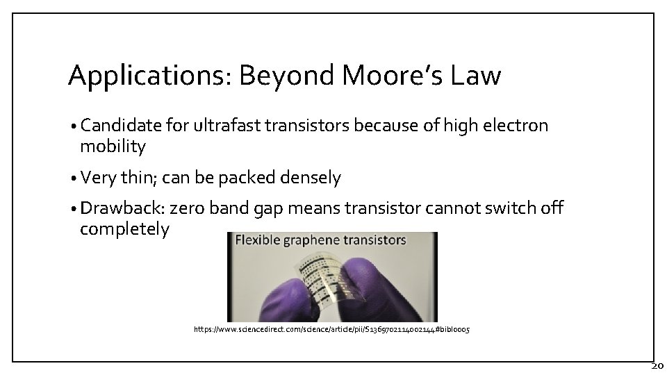
Applications: Beyond Moore’s Law • Candidate for ultrafast transistors because of high electron mobility • Very thin; can be packed densely • Drawback: zero band gap means transistor cannot switch off completely https: //www. sciencedirect. com/science/article/pii/S 1369702114002144#bibl 0005 20
Applications: Flexible Electronics • Could supplement or replace indium tin oxide (ITO) in touch screens, liquid crystal displays (LCDs), and organic light-emitting diodes (OLEDs) • Almost transparent (transmits 97. 7% of light) and conducts electricity well: two requirements • Strength and flexibility may allow it to be used in rollable e- paper, portable televisions, etc. , unlike ITO 21
Applications: Ultrafiltration • Honeycomb lattice allows water to pass through but keeps almost everything else out • 5 nm pore size graphene filter has been made (current state of the art is 30 -40 nm) • Thinness of graphene means less water pressure is needed during ultrafiltration 22
Applications: Composite Materials • Very strong and light compared to current carbon fiber technology • Can be used to make lighter aircraft • Conductivity means a graphene-coated aircraft could be protected against lightning 23
Recap • 2 D sheet of carbon atoms in a honeycomb lattice • Surprisingly, can be exfoliated from graphite and remain stable • Strength from strong σ bonds, interesting electrical properties from π bonds made possible by 2 D shape • Testbed for QED and other fascinating physics; under active study today • Many potential applications • All of the above made the isolation and characterization of graphene Nobel Prize-worthy 24
References Castro Neto, A. H. , et al. “The Electronic Properties of Graphene. ” Reviews of Modern Physics, vol. 81, no. 1, 14 Jan. 2009, pp. 109– 162. , doi: 10. 1103/Rev. Mod. Phys. 81. 109. de La Fuente, Jesus. “Graphene Applications & Uses. ” Graphenea, www. graphenea. com/pages/graphene-uses-applications#. Wv. F 9 w. Yjw. Y 2 w. de La Fuente, Jesus. “Publications. ” Graphenea, www. graphenea. com/pages/graphene-properties#. Wv. GITYjw. Y 2 w. Geim, Andrey K. , and Allan H. Mac. Donald. “Graphene: Exploring Carbon Flatland. ” Physics Today, vol. 60, no. 8, Aug. 2007, pp. 35– 41. , doi: 10. 1063/1. 2774096. Gibney, Elizabeth. “Surprise Graphene Discovery Could Unlock Secrets of Superconductivity. ” Scientific American, 7 Mar. 2018, www. scientificamerican. com/article/surprise-graphene-discovery-could-unlock-secrets-of-superconductivity/. “Graphene. ” Nobel. Prize. org, Royal Swedish Academy of Sciences, 5 Oct. 2010, www. nobelprize. org/nobel_prizes/physics/laureates/2010/advancedphysicsprize 2010. pdf. “Graphene. ” Quantum Made Simple, Physics Reimagined, 2018, toutestquantique. fr/en/graphene/. Leggett, Anthony J. “Lecture 5: Graphene: Electronic Band Structure and Dirac Fermions. ” Phys 769: Selected Topics in Condensed Matter Physics. 2010, University of Waterloo. Mc. Rae, Mike. “Strange Atomic Ripples in Graphene Could Unlock Clean, Limitless Energy. ” Science. Alert, 24 Nov. 2017, www. sciencealert. com/graphene-levy-flightslimitless-power-future-electronic-devices. Randviir, Edward P. , et al. “A Decade of Graphene Research: Production, Applications and Outlook. ” Materials Today, vol. 17, no. 9, Nov. 2014, pp. 426– 432. , doi: 10. 1016/j. mattod. 2014. 06. 001. Robinson, Ben. “Electrons Flowing like Liquid in Graphene Start a New Wave of Physics. ” Phys. org, 22 Aug. 2017, phys. org/news/2017 -08 -electrons-liquid-graphenephysics. html. Si - Silicon. www. ioffe. ru/SVA/NSM/Semicond/Si/electric. html. Sullivan, Michael. “Tight-Binding Model for Graphene. ” University of Manchester, 2017. “Valence Bond Theory. ” Lumen: Boundless Chemistry, Open SUNY Textbooks, courses. lumenlearning. com/boundless-chemistry/chapter/valence-bond-theory/. Young, Andrea F. , and Philip Kim. “Quantum Interference and Klein Tunnelling in Graphene Heterojunctions. ” Nature Physics, vol. 5, no. 3, 1 Feb. 2009, pp. 222– 226. , doi: 10. 1038/nphys 1198. 25