Good pattern placement Small feature sizes Reduced exposure
- Slides: 10

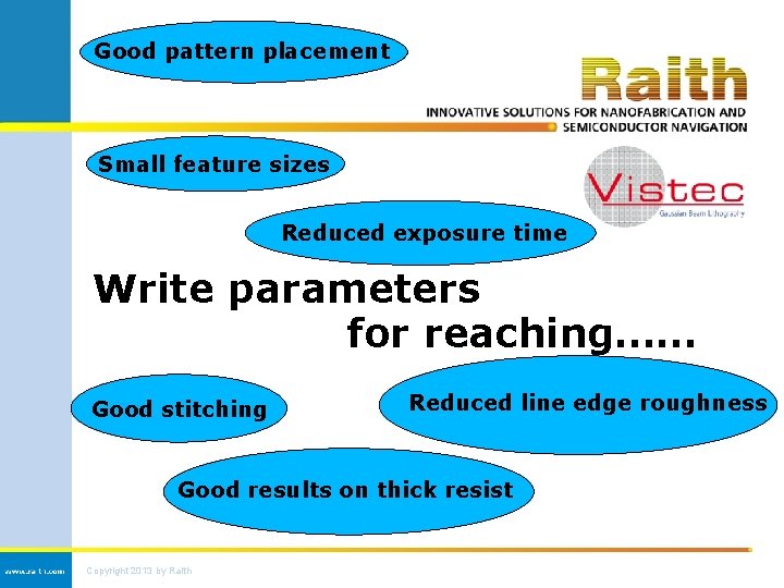
Good pattern placement Small feature sizes Reduced exposure time Write parameters for reaching…… Good stitching Reduced line edge roughness Good results on thick resist Copyright 2013 by Raith

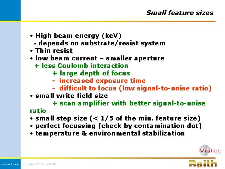
Small feature sizes • High beam energy (ke. V) § depends on substrate/resist system • Thin resist • low beam current – smaller aperture + less Coulomb interaction + large depth of focus - increased exposure time - difficult to focus (low signal-to-noise ratio) • small write field size + scan amplifier with better signal-to-noise ratio • small step size (< 1/5 of the min. feature size) • perfect focussing (check by contamination dot) • temperature & environmental stabilization Copyright 2013 by Raith

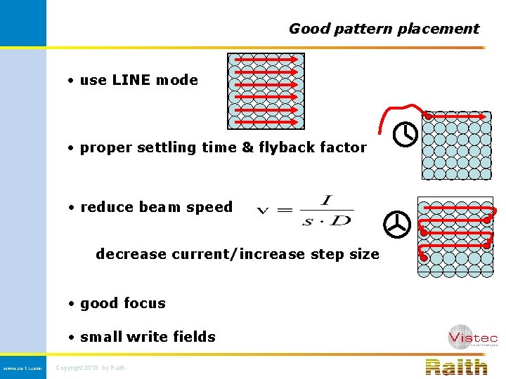
Good pattern placement • use LINE mode • proper settling time & flyback factor • reduce beam speed decrease current/increase step size • good focus • small write fields Copyright 2013 by Raith

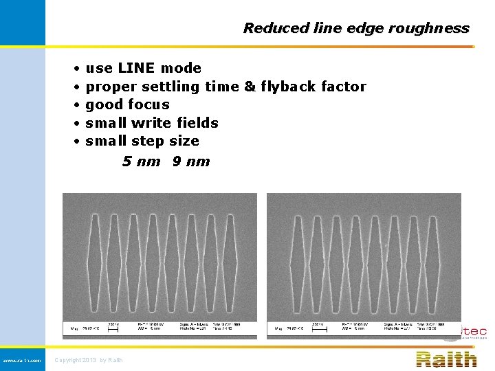
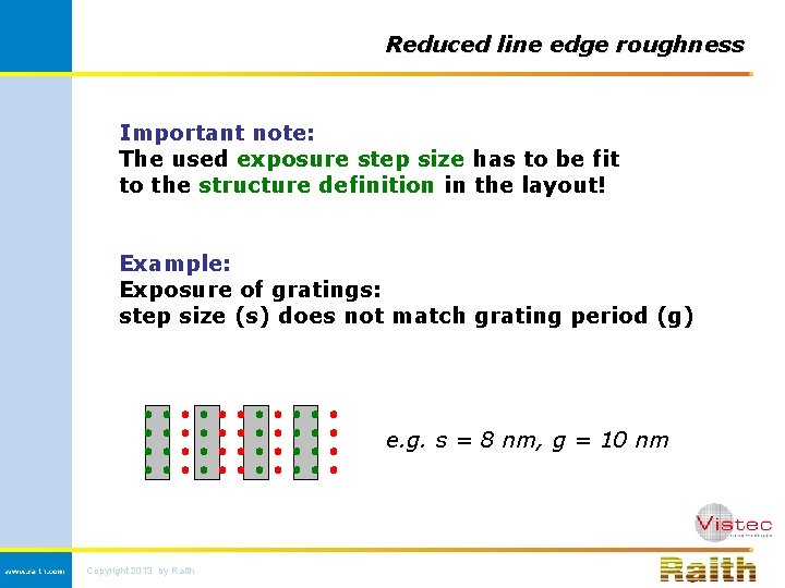
Reduced line edge roughness • • • use LINE mode proper settling time & flyback factor good focus small write fields small step size 5 nm 9 nm Copyright 2013 by Raith

Reduced line edge roughness Important note: The used exposure step size has to be fit to the structure definition in the layout! Example: Exposure of gratings: step size (s) does not match grating period (g) e. g. s = 8 nm, g = 10 nm Copyright 2013 by Raith

Reduced exposure time • meander mode (with flyback factor of 0. 01) • low settling time - less placement accuracy (high beam speed) • high beam current - less placement accuracy (high beam speed) • low beam energy (ke. V) + higher resist sensitivity (lower clearing dose) • large write fields + minimum stage travel - less resolution, distortion, low signal-to-noise Copyright 2013 by Raith

Good stitching • avoid mechanical drift wait after sample loading until system is stable • avoid beam drift wait after starting the gun and EHT on • take care of good zoom corrections from 0. 9999 to 1. 0001 (= 10 nm in 100 µm WF!) e. g. for 100 µm write field: => 2 successive write field alignments with 0. 5 µm marks and 45 µm stage travel => write field alignment next to exposure field Copyright 2013 by Raith

Good results on thick resist Critical issue: Undercut due to forward scattering in resist In order to avoid undercut … • use high ke. V • use resist with high contrast • avoid overexposure and overdeveloping § determine clearing dose very carefully § optimize developing process with respect to time and temperature Copyright 2013 by Raith

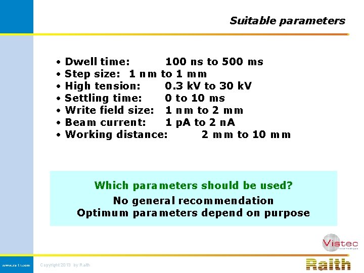
Suitable parameters • • Dwell time: 100 ns to 500 ms Step size: 1 nm to 1 mm High tension: 0. 3 k. V to 30 k. V Settling time: 0 to 10 ms Write field size: 1 nm to 2 mm Beam current: 1 p. A to 2 n. A Working distance: 2 mm to 10 mm Which parameters should be used? No general recommendation Optimum parameters depend on purpose Copyright 2013 by Raith

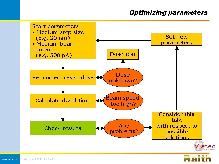
Optimizing parameters Start parameters • Medium step size (e. g. 20 nm) • Medium beam current (e. g. 300 p. A) Set new parameters Dose test Set correct resist dose Dose unknown? Calculate dwell time Beam speed too high? Check results Copyright 2013 by Raith Any problems? Consider this talk with respect to possible solutions