GEORGIAN TECHNICAL UNIVERSITY GTU knowledge is the power


- Slides: 71

GEORGIAN TECHNICAL UNIVERSITY GTU knowledge is the power …

Tecnology of Thin Films Laboratory of electronic materials tecnology Head of laboratory Full professor Zaur Jabua

What is thin film? Thin films can be solid or liquid (is more rare — gaseous). We will be further speaks about solid Thin Films The concept a “Thin Film” is relative Thin films — thin layers of the material, which thickness is in a range from nanometer shares (a mononuclear layer) to several microns

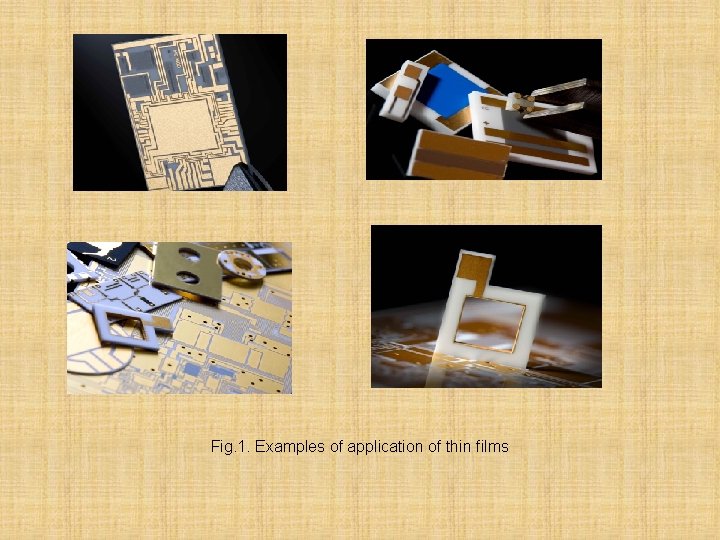
Why thin films draw attention? Often properties of thin films differ from properties of volume samples Thin Films find wide application in microelectronics, optics, in devices for measurement of small electric, magnetic and thermal fields, for receiving ultralow temperatures by an adiabatikelly degaussing etc.

Fig. 1. Examples of application of thin films

Thin films on the physical properties can will cause a stir from properties of the same materials in a massive condition. It creates additional problems when using films as technical materials and elements of equipment but on the other hand essentially expands possibilities of their practical application

It appeared that the objects having so small sizes, cardinally change the properties. For example, at so small objects the melting temperature, extent of overcooling and interplane distance in comparison with massive objects changes.

The Fenomologikal thermodynamics explains so unusual properties increase in a role of a surface with object reduction, after all at reduction of the size of a body its volume decreases in proportion degree 3, and the surface area — 2. Respectively the relation of V/S behaves as 1/r.

Thanks to it forces of a superficial tension which in massive samples don't play an essential role, in thin films become essential. And as forces of a superficial tension operate in a superficial layer, it is possible to assimilate their action to the appendix of external pressure which, as we know, can change both melting temperature, and interplane distances. As an example we will consider properties of thin films of copper

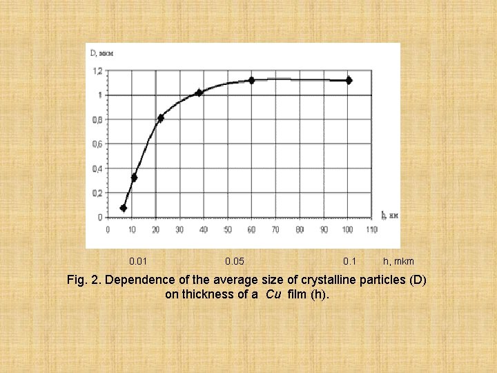
It is established that the copper film in thickness about 5 nanometers (0. 005 mkm) consists of crystalline particles which exist in the form of separate colonies and don't form a continuous covering. The average size of crystalline particles makes 0, 05 microns. The considerable disorder in the sizes of the separate crystalline particles, reaching 0, 025 microns is observed.

The copper film in thickness of 13 nanometers (0. 013 mkm) is already continuous and consists of large crystals with the average size of 0, 24 microns. Thicker film (21 nanometer= 0. 021 mkm) has the large size of crystalline particles - 0, 81 microns. The increase in the size of crystalline particles is observed with growth of thickness of a film to 60 nanometers (0. 060 mkm). Further the size of crystalline particles remains almost constant. On fig. 2. Is show dependence of the average size of crystalline particles (D) on thickness of a film (h).

0. 01 0. 05 0. 1 h, mkm Fig. 2. Dependence of the average size of crystalline particles (D) on thickness of a Cu film (h).

it is possible to assume that film formation on an amorphous substrate to occur in three stages 1) origin of separate crystalline particles, 2) growth of crystalline particles before their contact, education at first separate colonies, then a continuous film, 3) building layers to preservation of the constant cross-section size of crystalline particles. On fig. 3. is present dependence of specific electroresistance of a copper film on thickness.

It is visible that At thickness of a film more than 60 nanometers (0. 060 mkm) she behaves like the massive electric conductor, i. e. specific electric resistance doesn't depend on a large-scale factor thickness of a film. At thickness of a film its less than 60 nanometers (0. 060 mkm) with the full the basis it is possible to carry to the category of “Thin" Films since a material constant - specific electric resistance appears dependent on thickness of a film. With its reduction electric resistance sharply increass.

At thickness of a film its less than 60 nanometers (0. 060 mkm) with the full the basis it is possible to carry to the category of “Thin" Films since a material constant - specific electric resistance appears dependent on thickness of a film. With its reduction electric resistance sharply increases.

High electric resistance of “Thin" Films is caused by additional dispersion of electrons on borders of films if their thickness is commensurable with length of free run of electrons of conductivity. Dispersion of electrons arises also on borders of crystalline particles, especially, when their sizes - nanometer, and, therefore, the boundary area with the disorder arrangement of atoms occupies considerable volume of a film.

Let's consider some methods of preparation of films. There are some ways of preparation of thin films. From them it is conditionally possible to allocate two ways: CVD PVD Chemical vapor deposition (CVD) is a chemical process used to produce high-purity, high-performance solid materials. The process is often used in the semiconductor industry to produce thin films. In a typical CVD process, the wafer (substrate) is exposed to one or more volatile precursors, which react and/or decompose on the substrate surface to produce the desired deposit. Frequently, volatile by-products are also produced, which are removed by gas flow through the reaction chamber.

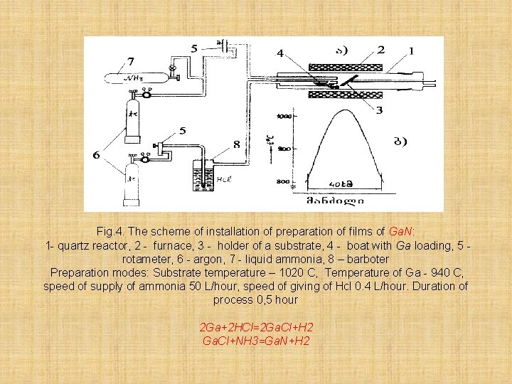
Physical vapor deposition (PVD) is a variety of vacuum deposition and is a general term used to describe any of a variety of methods to deposit thin films by the condensation of a vaporized form of the desired film material onto various workpiece surfaces (e. g. , onto semiconductor wafers). On fig. 4. is provided the scheme of installation of preparation of films of Ga. N by a method of a CVD

Fig. 4. The scheme of installation of preparation of films of Ga. N: 1 - quartz reactor, 2 - furnace, 3 - holder of a substrate, 4 - boat with Ga loading, 5 rotameter, 6 - argon, 7 - liquid ammonia, 8 – barboter Preparation modes: Substrate temperature – 1020 C, Temperature of Ga - 940 C, speed of supply of ammonia 50 L/hour, speed of giving of Hcl 0. 4 L/hour. Duration of process 0, 5 hour 2 Ga+2 HCl=2 Ga. Cl+H 2 Ga. Cl+NH 3=Ga. N+H 2

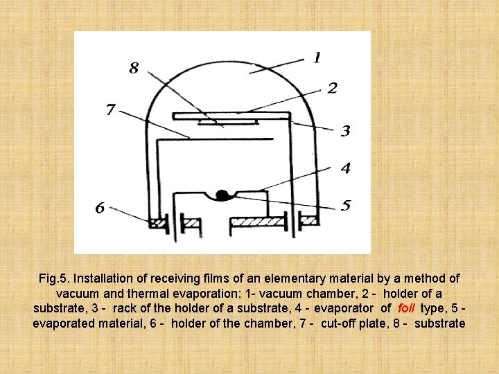
On fig. 5. is provided the scheme of installation of preparation of films by a method of a PVD

Fig. 5. Installation of receiving films of an elementary material by a method of vacuum and thermal evaporation: 1 - vacuum chamber, 2 - holder of a substrate, 3 - rack of the holder of a substrate, 4 - evaporator of foil type, 5 evaporated material, 6 - holder of the chamber, 7 - cut-off plate, 8 - substrate

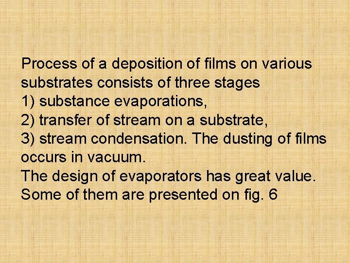
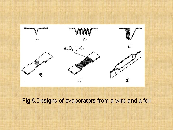
Process of a deposition of films on various substrates consists of three stages 1) substance evaporations, 2) transfer of stream on a substrate, 3) stream condensation. The dusting of films occurs in vacuum. The design of evaporators has great value. Some of them are presented on fig. 6

Fig. 6. Designs of evaporators from a wire and a foil

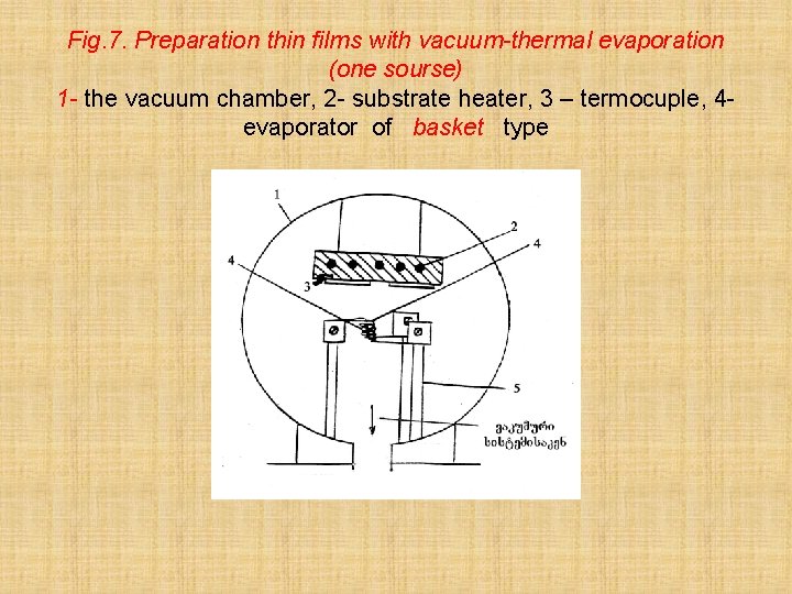
Fig. 7. Preparation thin films with vacuum-thermal evaporation (one sourse) 1 - the vacuum chamber, 2 - substrate heater, 3 – termocuple, 4 evaporator of basket type

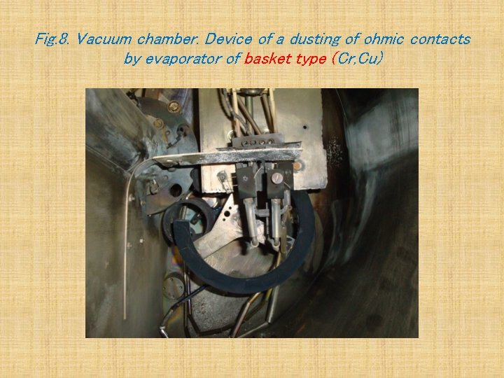
Fig. 8. Vacuum chamber. Device of a dusting of ohmic contacts by evaporator of basket type (Cr, Cu)

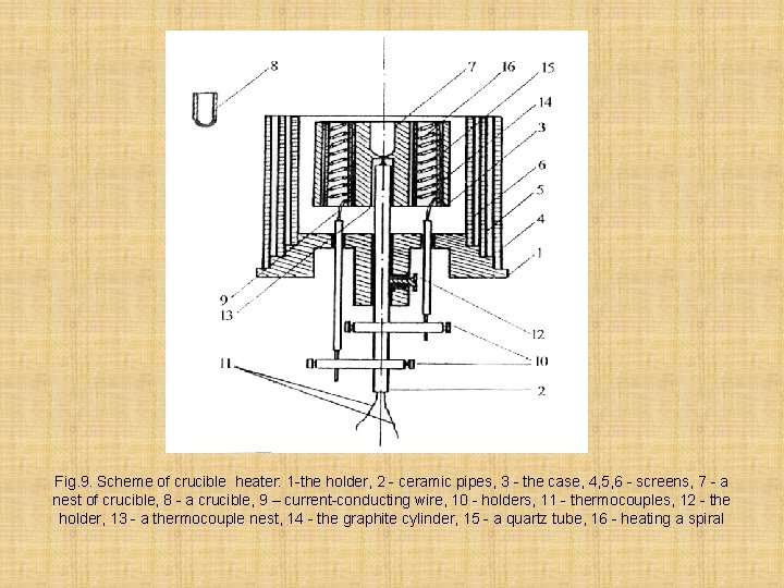
Wire evaporators as well as foil, don't give a stable stream, therefore apply crucible evaporators, which give the stable directed stream of of the evaporated substance are widely applied. The design of such evaporator is given on fig. 9. At a dusting the great value has constancy of temperature of a substrate.

Fig. 9. Scheme of crucible heater: 1 -the holder, 2 - ceramic pipes, 3 - the case, 4, 5, 6 - screens, 7 - a nest of crucible, 8 - a crucible, 9 – current-conducting wire, 10 - holders, 11 - thermocouples, 12 - the holder, 13 - a thermocouple nest, 14 - the graphite cylinder, 15 - a quartz tube, 16 - heating a spiral

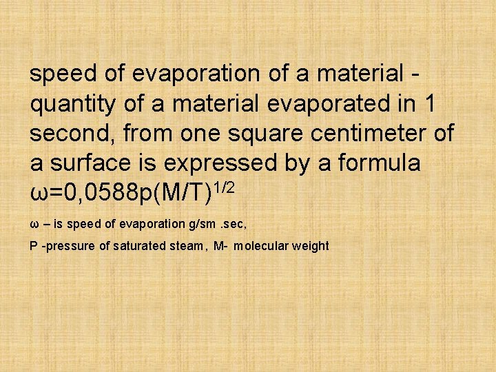
speed of evaporation of a material quantity of a material evaporated in 1 second, from one square centimeter of a surface is expressed by a formula ω=0, 0588 p(M/T)1/2 ω – is speed of evaporation g/sm. sec, P -pressure of saturated steam, M- molecular weight

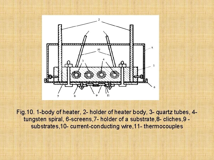
For a successful dusting of films the stable temperature of a substrate has great value. On fig. 10, the design of a heater of a substrate which we apply in our installations is given

Fig. 10. 1 -body of heater, 2 - holder of heater body, 3 - quartz tubes, 4 tungsten spiral, 6 -screens, 7 - holder of a substrate, 8 - cliches, 9 substrates, 10 - current-conducting wire, 11 - thermocouples

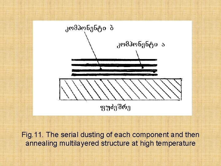
If preparation of thin films of an elementary material doesn't present a great difficulty, it it is impossible to tell about compund alloys. Often at heating occures their decomposition on making components. There are some methods of preparation of films of such materials: 1) the Serial dusting of each component and then annealing multilayered structure at high temperature, 2) Evaporation previously the synthesized material, 3) Simultaneous evaporation of components from different sources

Fig. 11. The serial dusting of each component and then annealing multilayered structure at high temperature

The first method - an alternate dusting and annealing, is applied to materials which are characterized by high diffusion of one material in another. Often this method receiving films of high uniformity isn't possible and consequently is applied seldom.

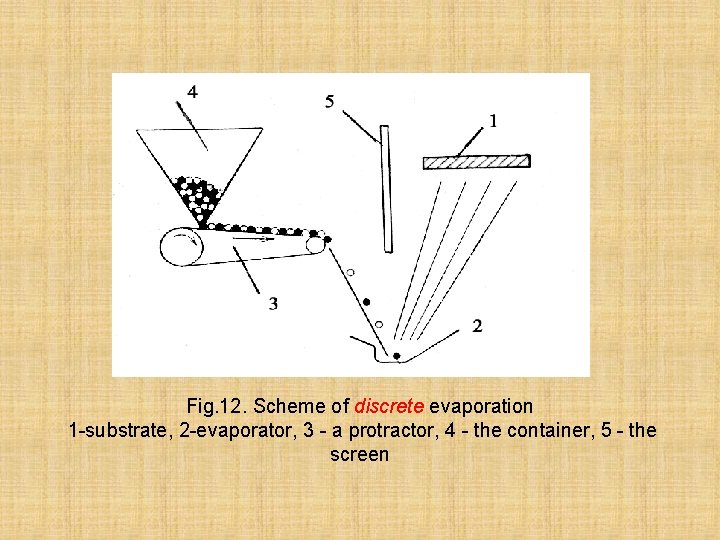
The second method - discrete evaporation - is applied to evaporation of alloys by which components have much speeds of evaporation differing from each other. In this method of a particle of the small sizes evenly move on previously heated-up evaporator and instantly evaporate without having been in time will go wrong

Fig. 12. Scheme of discrete evaporation 1 -substrate, 2 -evaporator, 3 - a protractor, 4 - the container, 5 - the screen

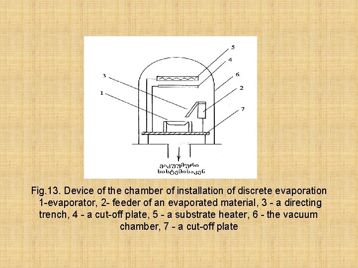
Fig. 13. Device of the chamber of installation of discrete evaporation 1 -evaporator, 2 - feeder of an evaporated material, 3 - a directing trench, 4 - a cut-off plate, 5 - a substrate heater, 6 - the vacuum chamber, 7 - a cut-off plate

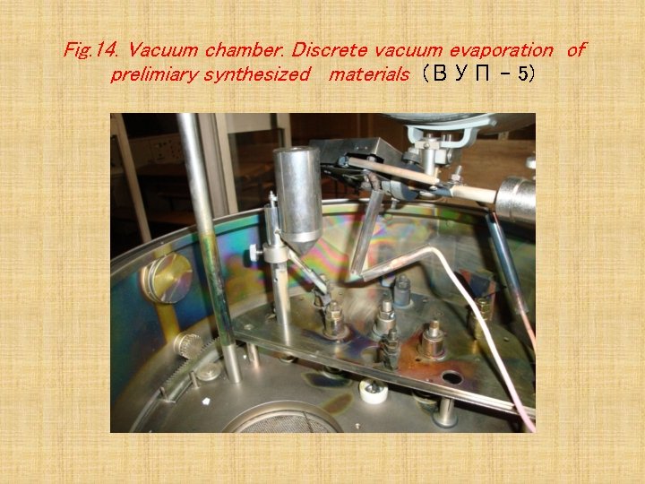
Fig. 14. Vacuum chamber. Discrete vacuum evaporation of prelimiary synthesized materials (ВУП – 5)

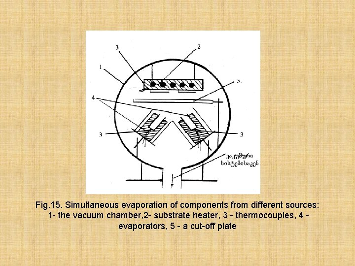
Еhe third method - simultaneous evaporation of components from two independent sources

Fig. 15. Simultaneous evaporation of components from different sources: 1 - the vacuum chamber, 2 - substrate heater, 3 - thermocouples, 4 evaporators, 5 - a cut-off plate

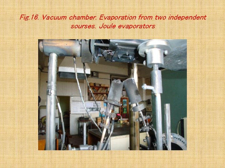
Fig. 16. Vacuum chamber. Evaporation from two independent sourses. Joule evaporators

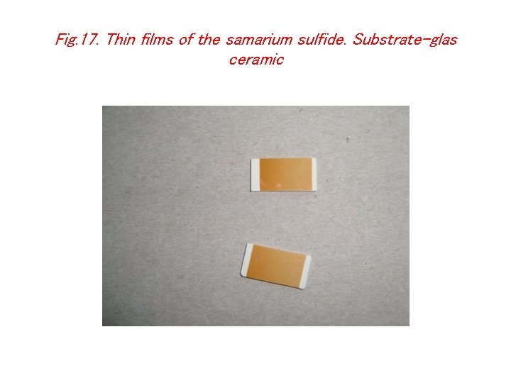
Fig. 17. Thin films of the samarium sulfide. Substrate-glas ceramic

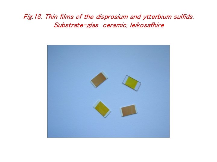
Fig. 18. Thin films of the disprosium and ytterbium sulfids. Substrate-glas ceramic, leikosafhire

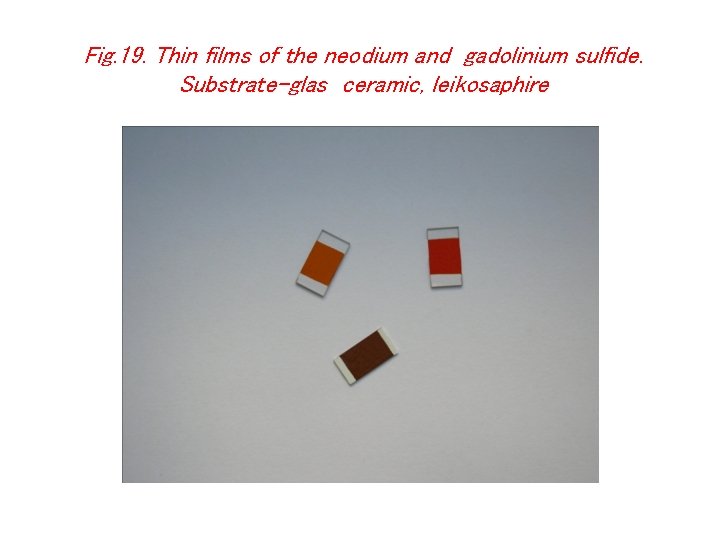
Fig. 19. Thin films of the neodium and gadolinium sulfide. Substrate-glas ceramic, leikosaphire

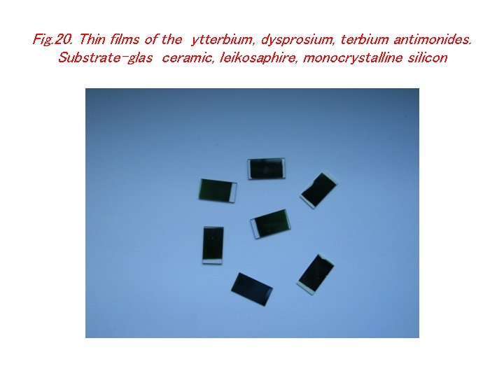
Fig. 20. Thin films of the ytterbium, dysprosium, terbium antimonides. Substrate-glas ceramic, leikosaphire, monocrystalline silicon

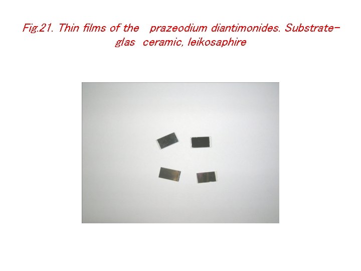
Fig. 21. Thin films of the prazeodium diantimonides. Substrateglas ceramic, leikosaphire

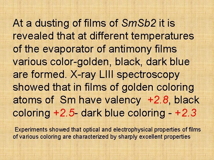
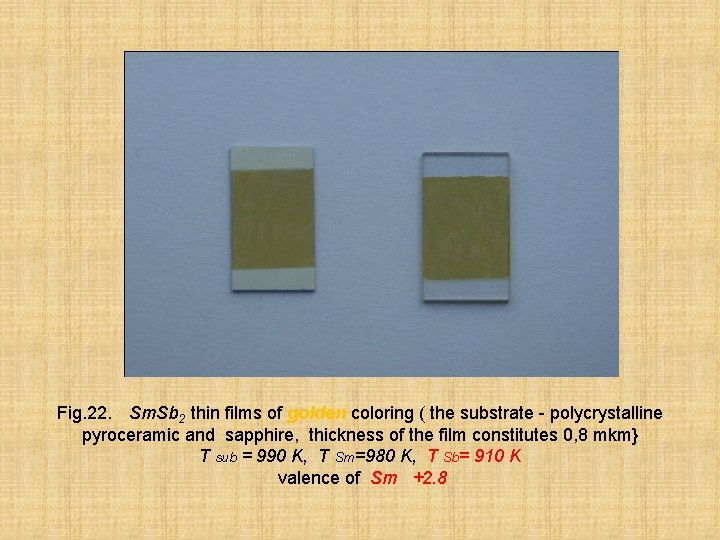
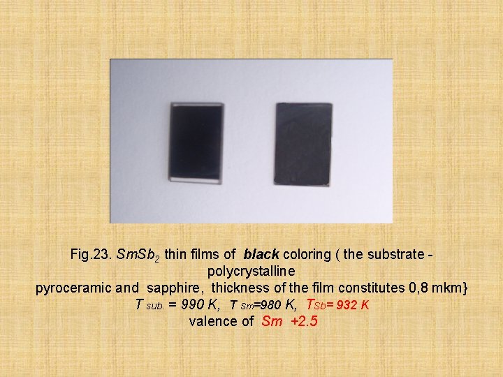
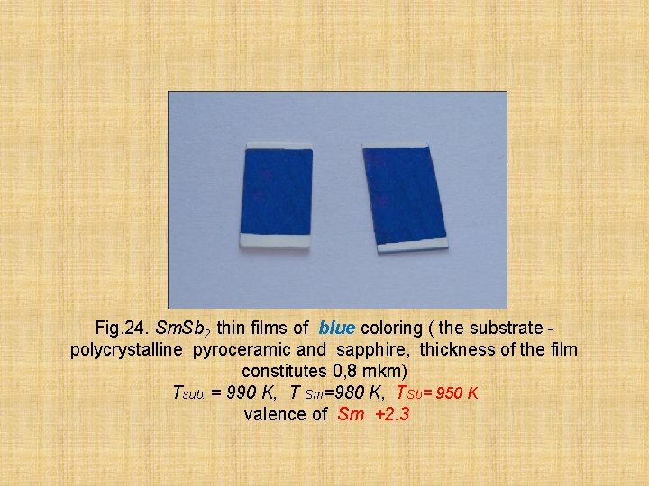
At a dusting of films of Sm. Sb 2 it is revealed that at different temperatures of the evaporator of antimony films various color-golden, black, dark blue are formed. X-ray LIII spectroscopy showed that in films of golden coloring atoms of Sm have valency +2. 8, black coloring +2. 5 - dark blue coloring - +2. 3 Experiments showed that optical and electrophysical properties of films of various coloring are characterized by sharply excellent properties

Fig. 22. Sm. Sb 2 thin films of golden coloring ( the substrate - polycrystalline pyroceramic and sapphire, thickness of the film constitutes 0, 8 mkm} T sub = 990 K, T Sm=980 K, T Sb= 910 K valence of Sm +2. 8

Fig. 23. Sm. Sb 2 thin films of black coloring ( the substrate polycrystalline pyroceramic and sapphire, thickness of the film constitutes 0, 8 mkm} T sub. = 990 K, T Sm=980 K, TSb= 932 K valence of Sm +2. 5

Fig. 24. Sm. Sb 2 thin films of blue coloring ( the substrate polycrystalline pyroceramic and sapphire, thickness of the film constitutes 0, 8 mkm) Tsub. = 990 K, T Sm=980 K, TSb= 950 K valence of Sm +2. 3

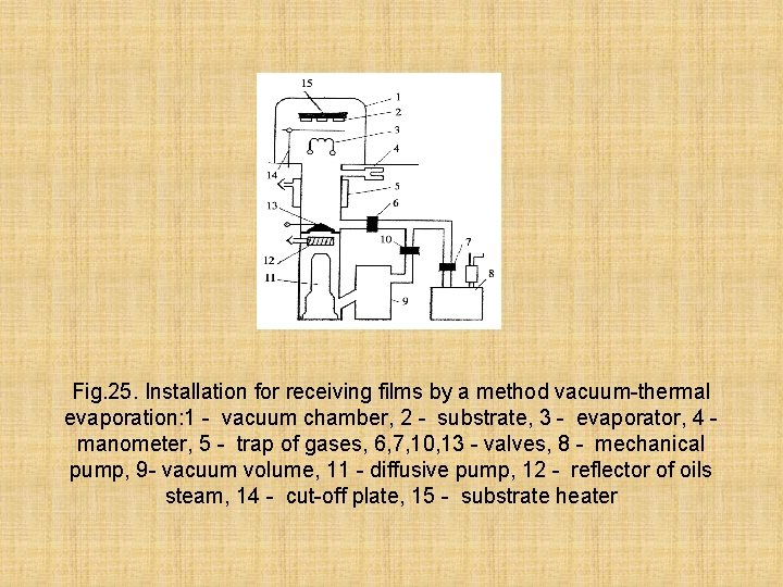
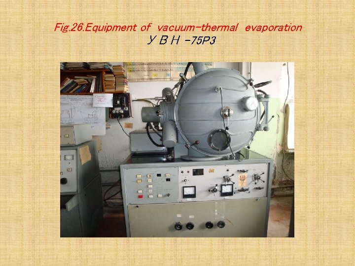
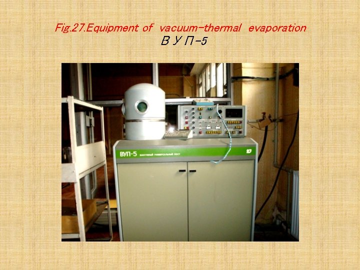
Below the scheme of installation of vacuum-thermal evaporation and the photo of installations used in our laboratory are provided

Fig. 25. Installation for receiving films by a method vacuum-thermal evaporation: 1 - vacuum chamber, 2 - substrate, 3 - evaporator, 4 manometer, 5 - trap of gases, 6, 7, 10, 13 - valves, 8 - mechanical pump, 9 - vacuum volume, 11 - diffusive pump, 12 - reflector of oils steam, 14 - cut-off plate, 15 - substrate heater

Fig. 26. Equipment of vacuum-thermal evaporation УВН -75 P 3

Fig. 27. Equipment of vacuum-thermal evaporation ВУП-5

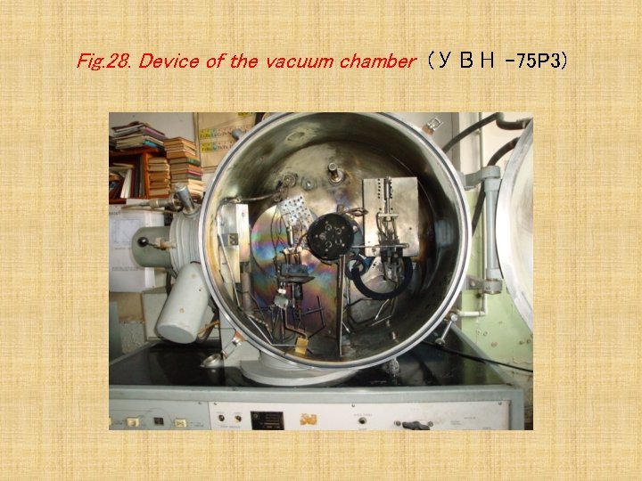
Fig. 28. Device of the vacuum chamber (УВН -75 P 3)

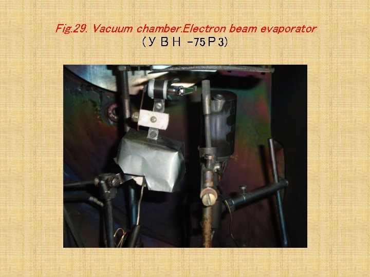
Fig. 29. Vacuum chamber. Electron beam evaporator (УВН -75 Р 3)

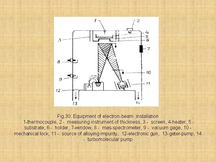
Let's consider the installation scheme for preparation of films by a method of an electron beam epitaxy. Elektron-beam epitaxy means evaporation and substance condensation at high vacuum. At this time the free length of atoms of steam is high and they from an evaporator to a substrate run over without collision. Advantage of this method is the low temperature of process that reduces probability of diffusion of impurity from a substrate. Besides this method it is characterized by smaller inertia in comparison with a airphase epitaxy, also allows will receive the composite profiles of a doping

Fig. 30. Equipment of electron-beam installation 1 -thermocouple, 2 - measuring instrument of thickness, 3 - screen, 4 -heater, 5 substrate, 6 - holder, 7 -window, 8 - mas-spectrometer, 9 - vacuum gage, 10 mechanical lock, 11 - source of alloying impurity, 12 -electronic gun, 13 -geter-pump, 14 - turbomolecular pump

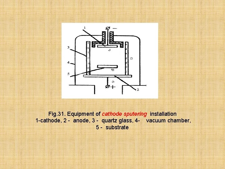
Often to preparation of films apply a method of cathodic and ionplasma evaporation of their scheme are provided on fig. 31 and fig. 32. A) Cathode sputering. In chamber are placed: the cathode made from evaporation material, the anode and a substrate. The chamber is filled with argon. Between the anode and the cathode tension of 1 -3 kilovolts is put. In the chamber there is a glow discharge. in the chamber atoms of argon are ionized and bombard the cathode, as a result of it the cathode and a material evaporates is besieged on a substrate. This method is applied to a dusting of films of materials which have high temperature of evaporation and a low elasticity steam.

Fig. 31. Equipment of cathode sputering installation 1 -cathode, 2 - anode, 3 - quartz glass, 4 - vacuum chamber, 5 - substrate

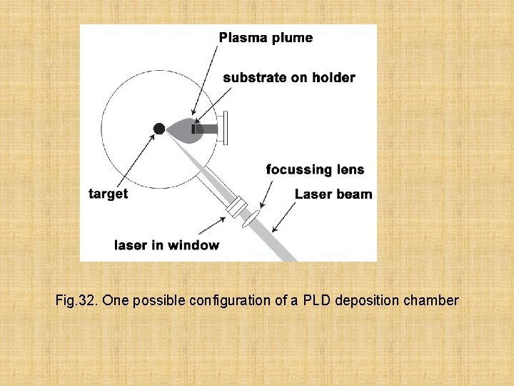
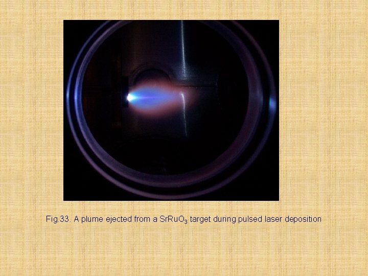
There is one more method of preparation of thin films a laser deposition (fig. 32) Pulsed laser deposition (PLD) is a thin film deposition (specifically a physical vapor deposition, PVD) technique where a high power pulsed laser beam is focused inside a vacuum chamber to strike a target of the material that is to be deposited. This material is vaporized from the target (in a plasma plume) which deposits it as a thin film on a substrate (such as a silicon wafer facing the target). This process can occur in ultra high vacuum or in the presence of a background gas, such as oxygen which is commonly used when depositing oxides to fully oxygenate the deposited films.

Fig. 32. One possible configuration of a PLD deposition chamber

Fig. 33. A plume ejected from a Sr. Ru. O 3 target during pulsed laser deposition

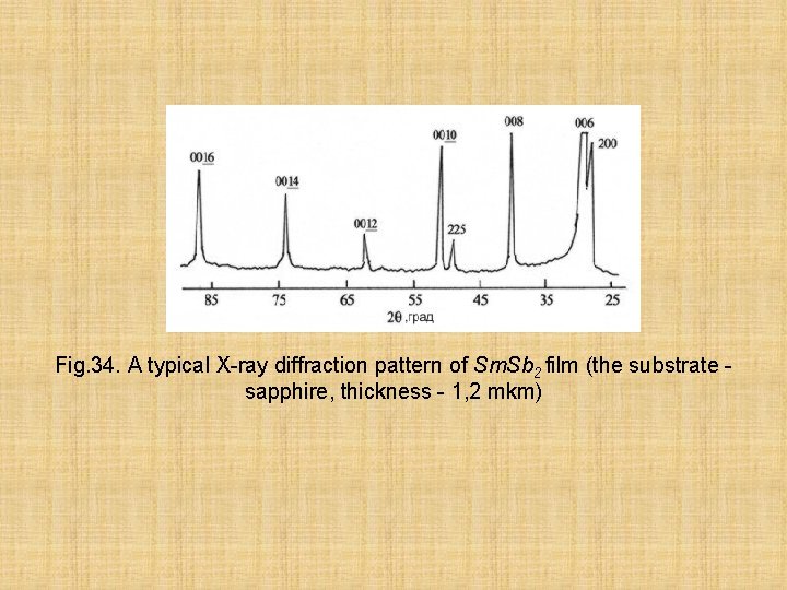
Methods of research of structure of films. There are some methods of studying of structure of films A) X-ray method; B) Electronographycal method; D) Tunnel microscopy

Fig. 34. A typical X-ray diffraction pattern of Sm. Sb 2 film (the substrate sapphire, thickness - 1, 2 mkm)

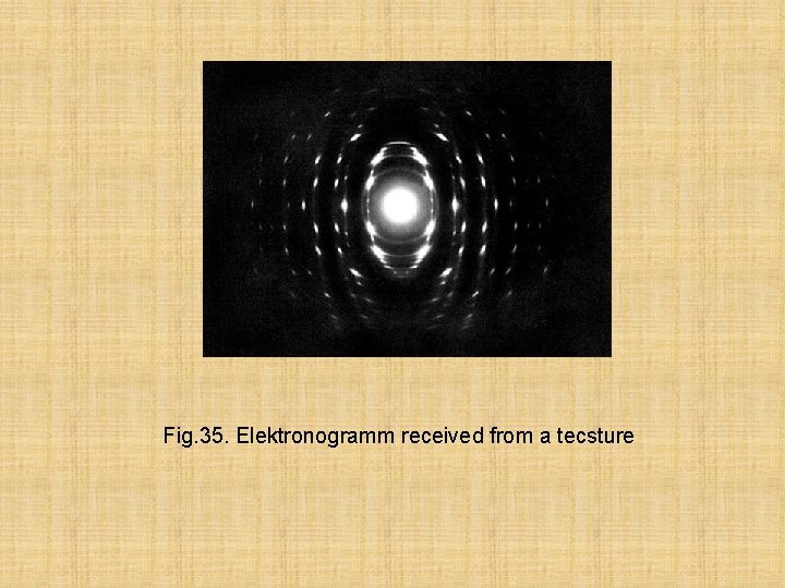
The electronographical method is applied to studying of structure of films. Elektronography is a method of studying of structure of the substance, based on dispersion of the accelerated electrons by a studied sample.

Fig. 35. Elektronogramm received from a tecsture

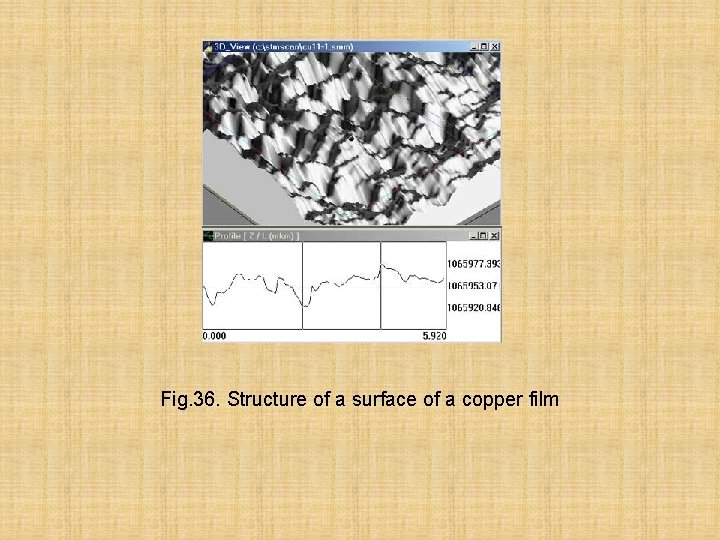
Ample opportunities of studying of structure of films appeared from the moment of emergence of the tunnel microscopy providing nanometer permission. On fig. 36 the microstructure of a film of copper received by a tunnel microscope is shown

Fig. 36. Structure of a surface of a copper film

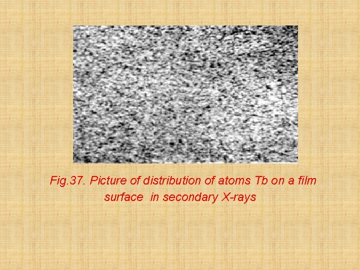
Fig. 37. Picture of distribution of atoms Tb on a film surface in secondary X-rays

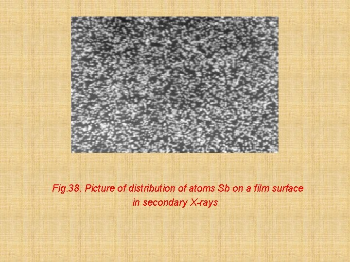
Fig. 38. Picture of distribution of atoms Sb on a film surface in secondary X-rays

Thanks for attention