General Semiconductor Packaging process flows Wafer Back Grinding
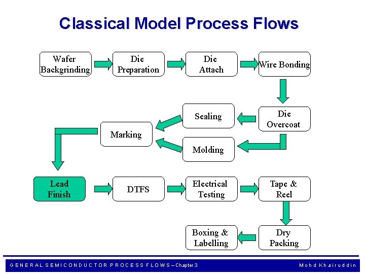
General Semiconductor Packaging process flows Wafer Back Grinding. Die Preparation. Die Attach. Wire Bonding. Die Overcoat. Molding. Sealing. Marking. DTFS (Deflash/Trim/Form/Singulation). Lead Finish. Electrical Testing. Tape and Reel. Dry Packing. Boxing and Labelling. G E N E R A L S E M I C O N D U C T O R P R O C E S S F L O W S – Chapter 3 Mohd Khairuddin
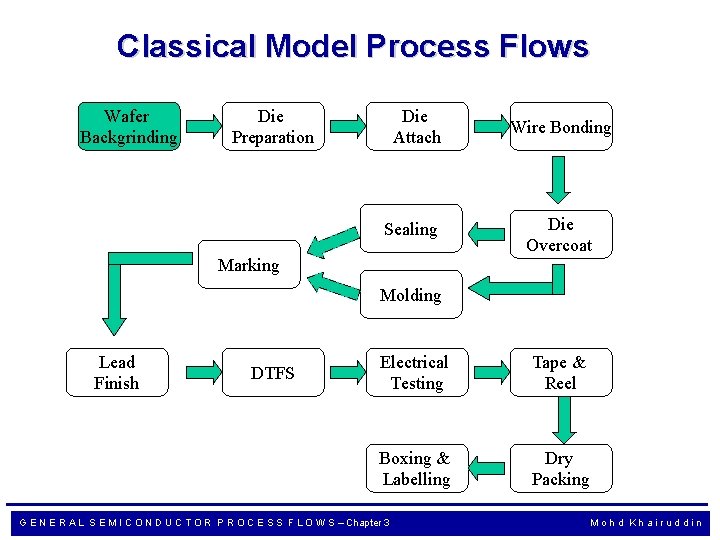
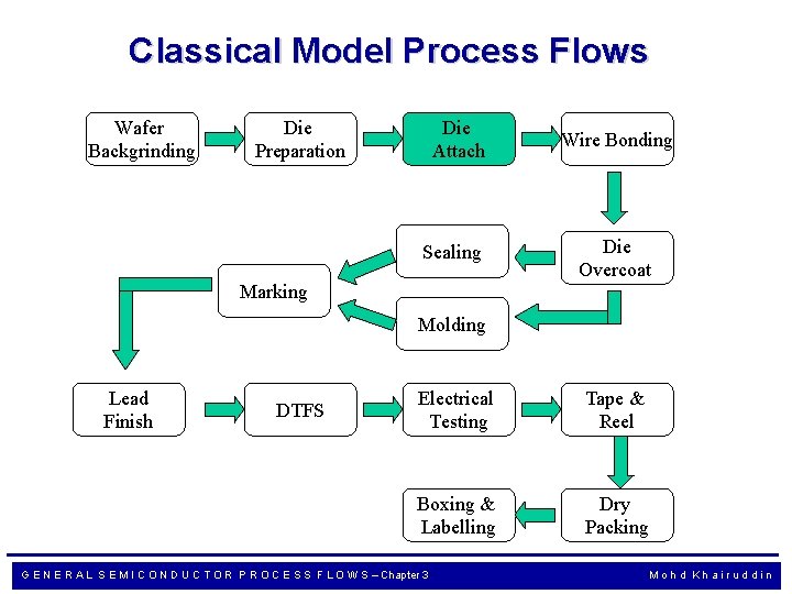
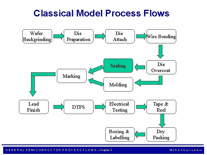
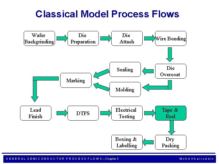
Classical Model Process Flows Wafer Backgrinding Die Preparation Die Attach Sealing Marking Wire Bonding Die Overcoat Molding Lead Finish DTFS Electrical Testing Tape & Reel Boxing & Labelling Dry Packing G E N E R A L S E M I C O N D U C T O R P R O C E S S F L O W S – Chapter 3 Mohd Khairuddin
Wafer Backgrinding • Is the process of grinding the backside of the wafer to the correct wafer thickness prior to assembly. Also referred to as 'wafer thinning. ' • Wafer backgrinding has not always been necessary, but the drive to make packages thinner and thinner has made it indispensable. Most package types in the semiconductor industry today would require a wafer thickness ranging from 8 mils (~200 µm) to 20 mils (~500 µm). Stacked die technology would require less than 100 µm. • Improves the transfer of heat from the front device side of the wafer to the backside, thus help to improve reliability. G E N E R A L S E M I C O N D U C T O R P R O C E S S F L O W S – Chapter 3 Mohd Khairuddin
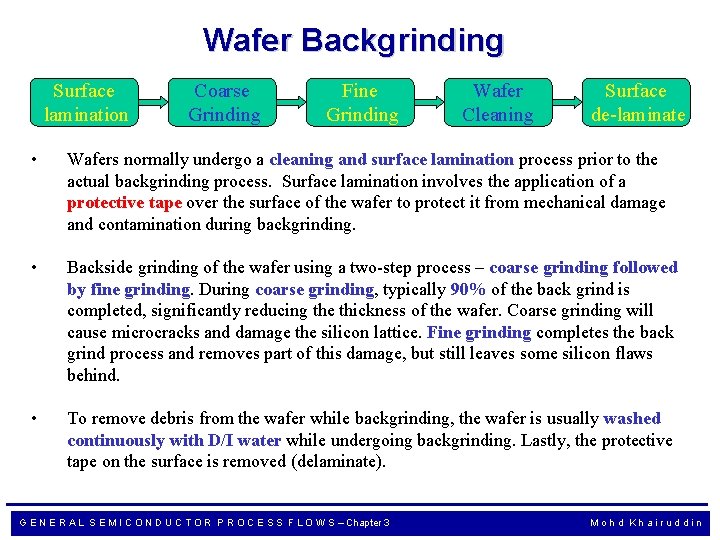
Wafer Backgrinding Surface lamination Coarse Grinding Fine Grinding Wafer Cleaning Surface de-laminate • Wafers normally undergo a cleaning and surface lamination process prior to the actual backgrinding process. Surface lamination involves the application of a protective tape over the surface of the wafer to protect it from mechanical damage and contamination during backgrinding. • Backside grinding of the wafer using a two-step process – coarse grinding followed by fine grinding. During coarse grinding, typically 90% of the back grind is completed, significantly reducing the thickness of the wafer. Coarse grinding will cause microcracks and damage the silicon lattice. Fine grinding completes the back grind process and removes part of this damage, but still leaves some silicon flaws behind. • To remove debris from the wafer while backgrinding, the wafer is usually washed continuously with D/I water while undergoing backgrinding. Lastly, the protective tape on the surface is removed (delaminate). G E N E R A L S E M I C O N D U C T O R P R O C E S S F L O W S – Chapter 3 Mohd Khairuddin
Important Parameters • Spindle speed - the rotational speed of the grinding wheel. • Spindle coolant water temperature and flow rate. • D/I water temperature, • Initial and final wafer thickness • Feed speeds - the feed rate of the grinding wheel toward the wafer. G E N E R A L S E M I C O N D U C T O R P R O C E S S F L O W S – Chapter 3 Mohd Khairuddin
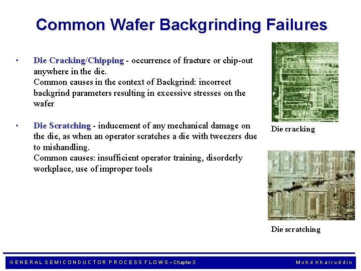
Common Wafer Backgrinding Failures • Die Cracking/Chipping - occurrence of fracture or chip-out anywhere in the die. Common causes in the context of Backgrind: incorrect backgrind parameters resulting in excessive stresses on the wafer • Die Scratching - inducement of any mechanical damage on the die, as when an operator scratches a die with tweezers due to mishandling. Common causes: insufficient operator training, disorderly workplace, use of improper tools Die cracking Die scratching G E N E R A L S E M I C O N D U C T O R P R O C E S S F L O W S – Chapter 3 Mohd Khairuddin
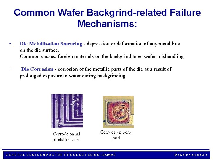
Common Wafer Backgrind-related Failure Mechanisms: • Die Metallization Smearing - depression or deformation of any metal line on the die surface. Common causes: foreign materials on the backgrind tape, wafer mishandling • Die Corrosion - corrosion of the metallic parts of the die as a result of prolonged exposure to water during backgrinding Corrode on Al metallization Corrode on bond pad G E N E R A L S E M I C O N D U C T O R P R O C E S S F L O W S – Chapter 3 Mohd Khairuddin
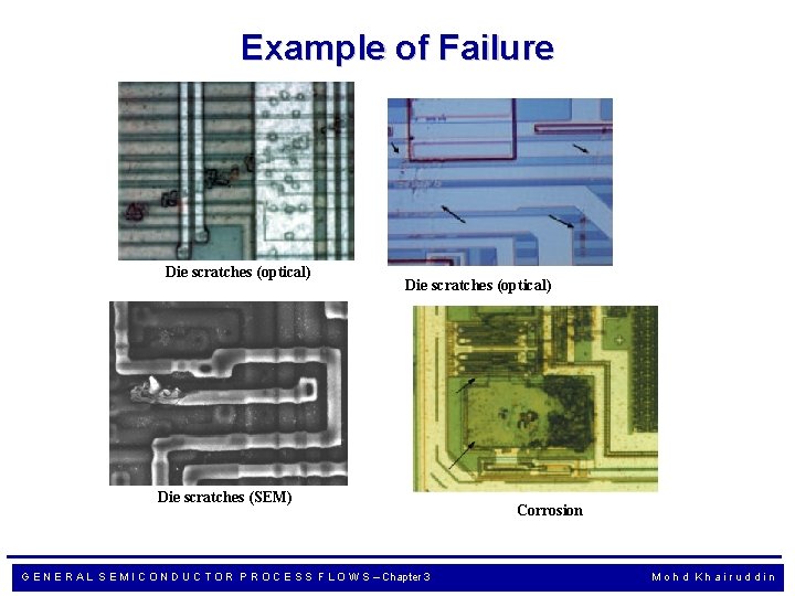
Example of Failure Die scratches (optical) Die scratches (SEM) G E N E R A L S E M I C O N D U C T O R P R O C E S S F L O W S – Chapter 3 Corrosion Mohd Khairuddin
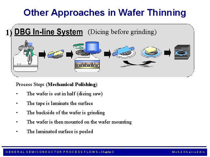
Other Approaches in Wafer Thinning (Dicing before grinding) 1) Process Step: (Mechanical Polishing) • The wafer is cut in half (dicing saw) • The tape is laminate the surface • The backside of the wafer is grinding • The wafer is then mounted on the wafer mounting • The laminated surface is peeled G E N E R A L S E M I C O N D U C T O R P R O C E S S F L O W S – Chapter 3 Mohd Khairuddin
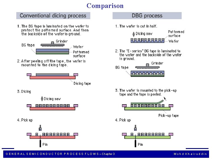
Comparison G E N E R A L S E M I C O N D U C T O R P R O C E S S F L O W S – Chapter 3 Mohd Khairuddin
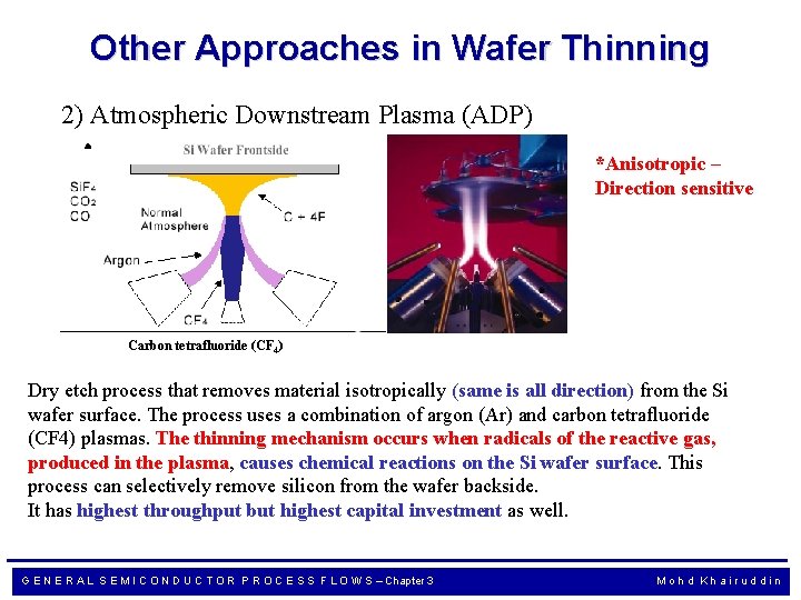
Other Approaches in Wafer Thinning 2) Atmospheric Downstream Plasma (ADP) *Anisotropic – Direction sensitive Carbon tetrafluoride (CF 4) Dry etch process that removes material isotropically (same is all direction) from the Si wafer surface. The process uses a combination of argon (Ar) and carbon tetrafluoride (CF 4) plasmas. The thinning mechanism occurs when radicals of the reactive gas, produced in the plasma, causes chemical reactions on the Si wafer surface. This process can selectively remove silicon from the wafer backside. It has highest throughput but highest capital investment as well. G E N E R A L S E M I C O N D U C T O R P R O C E S S F L O W S – Chapter 3 Mohd Khairuddin
Other Approaches in Wafer Thinning 3) Wet chemical etching A common technique to remove material stress free. To thin a whole wafer, a spin-spray etching mechanism has been developed. The process involves spraying an etching agent onto the surface of a rotating wafer periodically. Different chemical compositions of etching agents can give a wide variety of surface finishes, from a mirror-like surface finish to a very rough surface finish. The most common isotropic etching agent used for thinning Si wafers is a mixture of hydrofluoric acid (HF) and nitric acid (HNO 3). It has very fast etching rate in silicon, unfortunately 20 um thick silicon has to be removed in order to reach good thickness variation performance. So the throughput is not the highest among these three. G E N E R A L S E M I C O N D U C T O R P R O C E S S F L O W S – Chapter 3 Mohd Khairuddin
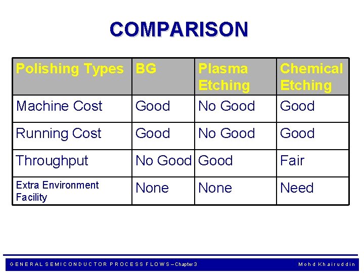
COMPARISON Polishing Types BG Machine Cost Good Plasma Etching No Good Running Cost Good No Good Throughput No Good Fair Extra Environment Facility None Need G E N E R A L S E M I C O N D U C T O R P R O C E S S F L O W S – Chapter 3 None Chemical Etching Good Mohd Khairuddin
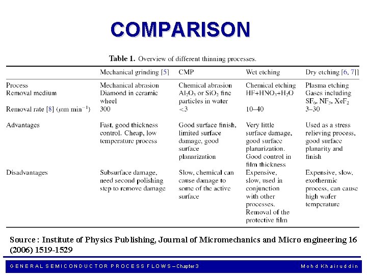
COMPARISON Source : Institute of Physics Publishing, Journal of Micromechanics and Micro engineering 16 (2006) 1519 -1529 G E N E R A L S E M I C O N D U C T O R P R O C E S S F L O W S – Chapter 3 Mohd Khairuddin
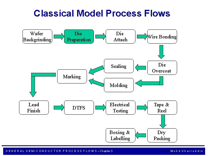
Classical Model Process Flows Wafer Backgrinding Die Preparation Die Attach Sealing Marking Wire Bonding Die Overcoat Molding Lead Finish DTFS Electrical Testing Tape & Reel Boxing & Labelling Dry Packing G E N E R A L S E M I C O N D U C T O R P R O C E S S F L O W S – Chapter 3 Mohd Khairuddin
Die Preparation Die preparation is the process by which the wafer is singulated into individual dice in preparation for assembly. Die preparation consists of two major steps, namely, wafer mounting and wafer saw, (other than wafer saw, people also use diamond scriber) During wafer mounting, the following concerns must be prevented: wafer cracking or breakage, bubble trapping on the adhesive side of the tape, scratches on the active side of the wafer, and non-uniform tape tension which can result in tape wrinkles. G E N E R A L S E M I C O N D U C T O R P R O C E S S F L O W S – Chapter 3 Mohd Khairuddin
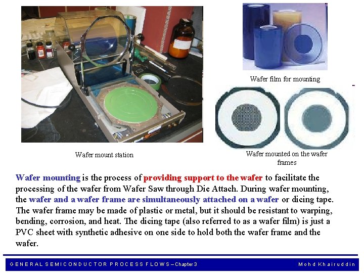
Wafer film for mounting Wafer mount station Wafer mounted on the wafer frames Wafer mounting is the process of providing support to the wafer to facilitate the processing of the wafer from Wafer Saw through Die Attach. During wafer mounting, the wafer and a wafer frame are simultaneously attached on a wafer or dicing tape. The wafer frame may be made of plastic or metal, but it should be resistant to warping, bending, corrosion, and heat. The dicing tape (also referred to as a wafer film) is just a PVC sheet with synthetic adhesive on one side to hold both the wafer frame and the wafer. G E N E R A L S E M I C O N D U C T O R P R O C E S S F L O W S – Chapter 3 Mohd Khairuddin
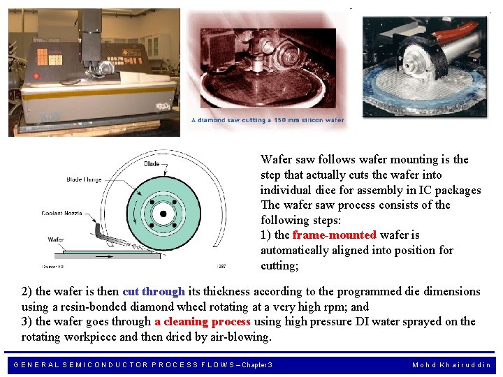
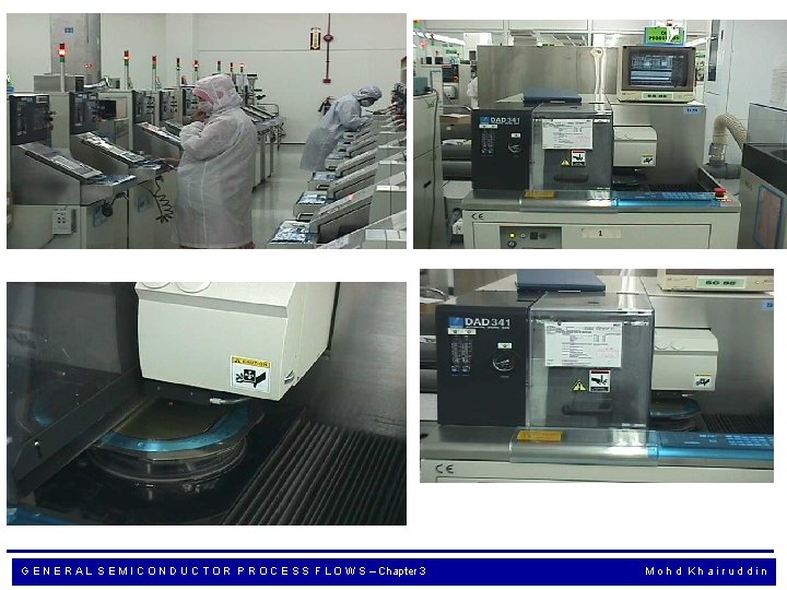
Wafer saw follows wafer mounting is the step that actually cuts the wafer into individual dice for assembly in IC packages The wafer saw process consists of the following steps: 1) the frame-mounted wafer is automatically aligned into position for cutting; 2) the wafer is then cut through its thickness according to the programmed die dimensions using a resin-bonded diamond wheel rotating at a very high rpm; and 3) the wafer goes through a cleaning process using high pressure DI water sprayed on the rotating workpiece and then dried by air-blowing. G E N E R A L S E M I C O N D U C T O R P R O C E S S F L O W S – Chapter 3 Mohd Khairuddin
G E N E R A L S E M I C O N D U C T O R P R O C E S S F L O W S – Chapter 3 Mohd Khairuddin
Important Parameters Important parameters for consideration during wafer saw include the following: • cut mode (direction and manner of cutting), • feed speed (speed at which the wafer is being introduced to the blade), spindle revolution (speed of revolution of the cutting wheel), • blade height, and • cutting water flow. Important parameters for the washing step include the following: wash time, wash rpm, DI water pressure, dry time, dry rpm, temperature and air flowrate. G E N E R A L S E M I C O N D U C T O R P R O C E S S F L O W S – Chapter 3 Mohd Khairuddin
Common Die Prep-related Failure Mechanisms: Die Lifting - detachment of the die from the die pad or cavity. Wafer backside contamination during die preparation may inhibit good adhesion between the die backside and the die attach material. Other common causes of Die Lifting: contamination on the die pad or cavity, excessive die attach voids, incomplete die attach coverage, inadequate die attach curing. Die Cracking - occurrence of fracture anywhere in the die. Incorrect wafer saw and washing parameters can result in microcracks in the wafers, which can propagate into larger die cracks during later stages of the assembly process. Other common causes of Die Cracking: excessive die attach voids, die overhang or insufficient die attach coverage, excessive die ejection force on the wafer tape. Die Contamination - contamination of the die surface with silicon dust or foreign material that may be attached either by electrostatic, mechanical, or chemical means. Common Causes: contaminated rinsing water; static charge G E N E R A L S E M I C O N D U C T O R P R O C E S S F L O W S – Chapter 3 Mohd Khairuddin
Common Die Prep-related Failure Mechanisms: Die Scratching - inducement of any mechanical damage on the die, as when an operator scratches a die with tweezers due to mishandling. Die scratches can also result from mishandling of wafers during the die preparation process. Other Common Causes of Die Scratching: insufficient operator training, disorderly workplace, use of improper tools. Die Metallization Smearing - depression or deformation of any metal line on the die surface. Common Causes: dirty or worn-out die attach pick-and-place tool, wafer mishandling Die Corrosion - corrosion of the metallization and other components of the die. Common Causes: corrosive contaminants on the wafer tape or rinsing water G E N E R A L S E M I C O N D U C T O R P R O C E S S F L O W S – Chapter 3 Mohd Khairuddin
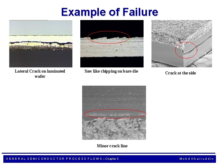
Example of Failure Lateral Crack on laminated wafer Saw like chipping on bare die Crack at the side Minor crack line G E N E R A L S E M I C O N D U C T O R P R O C E S S F L O W S – Chapter 3 Mohd Khairuddin
Classical Model Process Flows Wafer Backgrinding Die Preparation Die Attach Sealing Marking Wire Bonding Die Overcoat Molding Lead Finish DTFS Electrical Testing Tape & Reel Boxing & Labelling Dry Packing G E N E R A L S E M I C O N D U C T O R P R O C E S S F L O W S – Chapter 3 Mohd Khairuddin
Die Attach (also known as Die Mount or Die Bond) is the process of attaching the silicon chip to the die pad or die cavity of the support structure (e. g. , the leadframe) of the semiconductor package. There are three common die attach processes, i. e. , adhesive(epoxy) die attach, eutectic die attach and glass frit attach. These processes use special die attach equipment and die attach tools to mount the die. They also provide thermal and/or electrical conductivity between the die and the package, essentially affecting the performance of the device while operating in the field G E N E R A L S E M I C O N D U C T O R P R O C E S S F L O W S – Chapter 3 Mohd Khairuddin
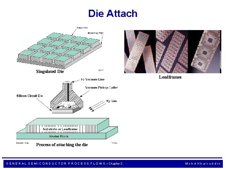
Die Attach Singulated Die Leadframes Process of attaching the die G E N E R A L S E M I C O N D U C T O R P R O C E S S F L O W S – Chapter 3 Mohd Khairuddin
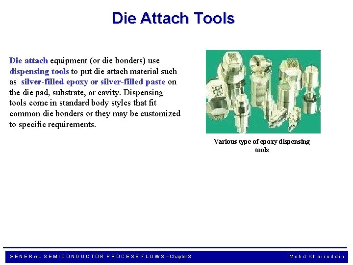
Die Attach Tools Die attach equipment (or die bonders) use dispensing tools to put die attach material such as silver-filled epoxy or silver-filled paste on the die pad, substrate, or cavity. Dispensing tools come in standard body styles that fit common die bonders or they may be customized to specific requirements. Various type of epoxy dispensing tools G E N E R A L S E M I C O N D U C T O R P R O C E S S F L O W S – Chapter 3 Mohd Khairuddin
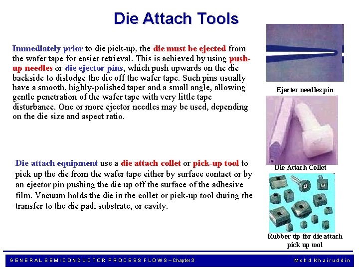
Die Attach Tools Immediately prior to die pick-up, the die must be ejected from the wafer tape for easier retrieval. This is achieved by using pushup needles or die ejector pins, which push upwards on the die backside to dislodge the die off the wafer tape. Such pins usually have a smooth, highly-polished taper and a small angle, allowing gentle penetration of the wafer tape with very little tape disturbance. One or more ejector needles may be used, depending on the die size and aspect ratio. Die attach equipment use a die attach collet or pick-up tool to pick up the die from the wafer tape either by surface contact or by an ejector pin pushing the die up off the surface of the adhesive film. Vacuum holds the die in the collet or pick-up tool during the transfer to the die pad, substrate, or cavity. Ejecter needles pin Die Attach Collet Rubber tip for die attach pick up tool G E N E R A L S E M I C O N D U C T O R P R O C E S S F L O W S – Chapter 3 Mohd Khairuddin
Adhesive (Epoxy) Die Attach The most common attach material is epoxy. It can be formulated with or without silver. If the attach only requires a mechanical connection with modest thermal demands, then a straight epoxy is used. The epoxy will be silver-filled if the attach requires either an electrical connection or a lower impedance thermal path. The majority of MOS products use straight epoxy. An appropriate heat cures the epoxy. Other than epoxy is polymide and silver-paste. Process - The adhesive is first dispensed in controlled amounts on the die pad or cavity. The die for mounting is then ejected from the wafer by one or more ejector needles. While being ejected, a pick-and-place tool commonly known as a 'collet' then retrieves the die from the wafer tape and positions it on the adhesive. All of the above steps are done by special die attach equipment or 'die bonders‘. G E N E R A L S E M I C O N D U C T O R P R O C E S S F L O W S – Chapter 3 Mohd Khairuddin
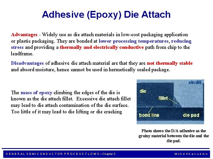
Adhesive (Epoxy) Die Attach Advantages - Widely use as die attach materials in low-cost packaging application or plastic packaging. They are bonded at lower processing temperatures, reducing stress and providing a thermally and electrically conductive path from chip to the leadframe. Disadvantages of adhesive die attach material are that they are not thermally stable and absord moisture, hence cannot be used in hermetically sealed package. The mass of epoxy climbing the edges of the die is known as the die attach fillet. Excessive die attach fillet may lead to die attach contamination of the die surface. Too little of it may lead to die lifting or die cracking Photo shows the D/A adhesive as the grainy material between the die and the die pad. G E N E R A L S E M I C O N D U C T O R P R O C E S S F L O W S – Chapter 3 Mohd Khairuddin
Eutectic Die Attach Eutectic die attach, which is commonly employed in hermetic packages, uses a eutectic alloy to attach the die to the cavity. A eutectic alloy is an alloy with the lowest melting point possible for the metals combined in the alloy. The Au-Si eutectic alloy is the most commonly used die attach alloy in semiconductor packaging. Process - For a eutectic attach, a thin film of gold is deposited on the back side of the wafer. This gold layer is alloyed into the silicon to form a Au-Si alloy. As more Si diffuses into the gold preform, the Si-to-Au ratio of the alloy increases, until such time that the eutectic ratio is achieved. Aside from the Au-Si alloy, semiconductor assembly may employ other metal alloys for eutectic die attach. Au-Sn; Pb-Ag-In; Pb-Sn; Au-Ge; Au G E N E R A L S E M I C O N D U C T O R P R O C E S S F L O W S – Chapter 3 Mohd Khairuddin
Eutectic Die Attach Advantages – provide good thermal path, mechanical strength, and electrical contact for backside bias voltages. Many bipolar ICs use this system. Disadvantages – higher stresses on the chip resulting from thermal expansion mismatch and lack of plastic flow. Au/Si (363 o. C), Au/Sn (280 o. C) G E N E R A L S E M I C O N D U C T O R P R O C E S S F L O W S – Chapter 3 Mohd Khairuddin
Glass Frit Attach The third alternative is to die attach with glass frit material. This material is generally used for die attach in ceramic packages that require a high-temperature hermetic seal. The glass frit system generally uses a silver-filled mixture. Advantages – thermally stable and can provide a void-free bond improving reliability and thermal management. Disadvantages – Require high bonding temperature (~400 °C), oxidizing environment for good adhesion and solvents leading to several processing concerns. G E N E R A L S E M I C O N D U C T O R P R O C E S S F L O W S – Chapter 3 Mohd Khairuddin
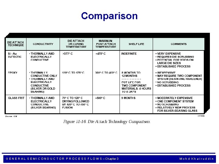
Comparison G E N E R A L S E M I C O N D U C T O R P R O C E S S F L O W S – Chapter 3 Mohd Khairuddin
Common Die Attach-related Failure Mechanisms Die Lifting - detachment of the die from the die pad or cavity. Common Causes: contamination on the die pad or cavity, die backside contamination, excessive die attach voids, incomplete die attach coverage, inadequate die attach curing. Die Cracking - occurrence of fracture anywhere in the die. Common Causes in the context of Die Attach: excessive die attach voids, die overhang or insufficient die attach coverage, insufficient bond line thickness, excessive die ejection force on the wafer tape, absence of die attach voids Adhesive Shorting - electrical shorting between exposed metal lines, bond pads, bonds, or wires as a result of adhesive accidentally dripping on the surface of the die (sometimes called 'epoxy on die'). Common Causes: incorrect die attach material viscosity, incorrect adhesive dispensation G E N E R A L S E M I C O N D U C T O R P R O C E S S F L O W S – Chapter 3 Mohd Khairuddin
Common Die Attach-related Failure Mechanisms Bond Lifting - lifting of the first or second bond from the die or leadfinger, respectively. From the die attach process point of view, this is often due to resin bleeding of the die attach material into the bond pads or leadfingers, inhibiting good intermetallic formation. See also Wirebonding. Die Scratching - inducement of any mechanical damage on the die, as when an operator scratches a die with tweezers due to mishandling. Common Causes: insufficient operator training, worn-out or contaminated pick-and-place tool, disorderly workplace, use of improper tools Die Metallization Smearing - depression or deformation of any metal line on the die surface. Common Causes: dirty or worn-out die attach pick-and-place tool, wafer mishandling G E N E R A L S E M I C O N D U C T O R P R O C E S S F L O W S – Chapter 3 Mohd Khairuddin
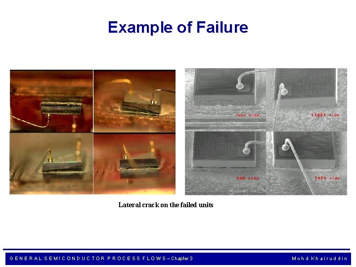
Example of Failure Lateral crack on the failed units G E N E R A L S E M I C O N D U C T O R P R O C E S S F L O W S – Chapter 3 Mohd Khairuddin
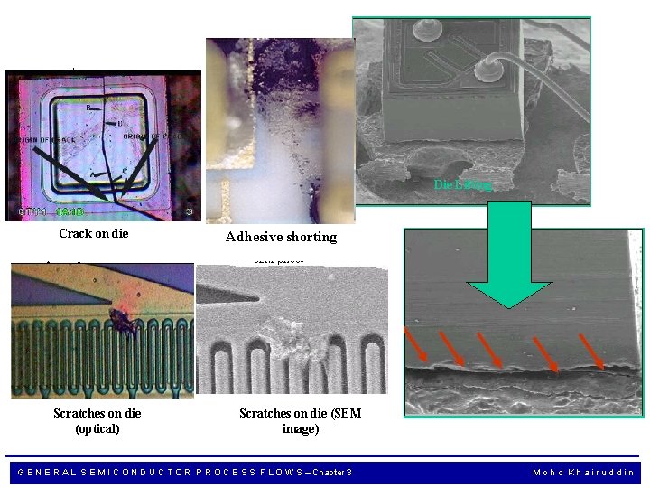
Die Lifting Crack on die Scratches on die (optical) Adhesive shorting Scratches on die (SEM image) G E N E R A L S E M I C O N D U C T O R P R O C E S S F L O W S – Chapter 3 Mohd Khairuddin
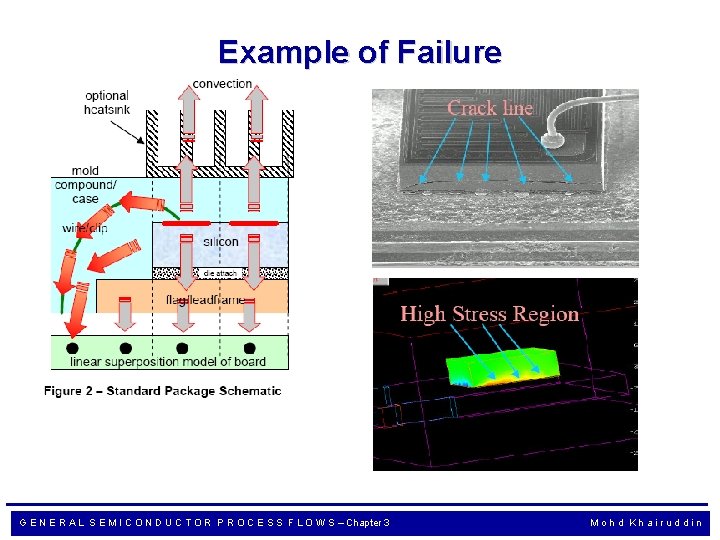
Example of Failure G E N E R A L S E M I C O N D U C T O R P R O C E S S F L O W S – Chapter 3 Mohd Khairuddin
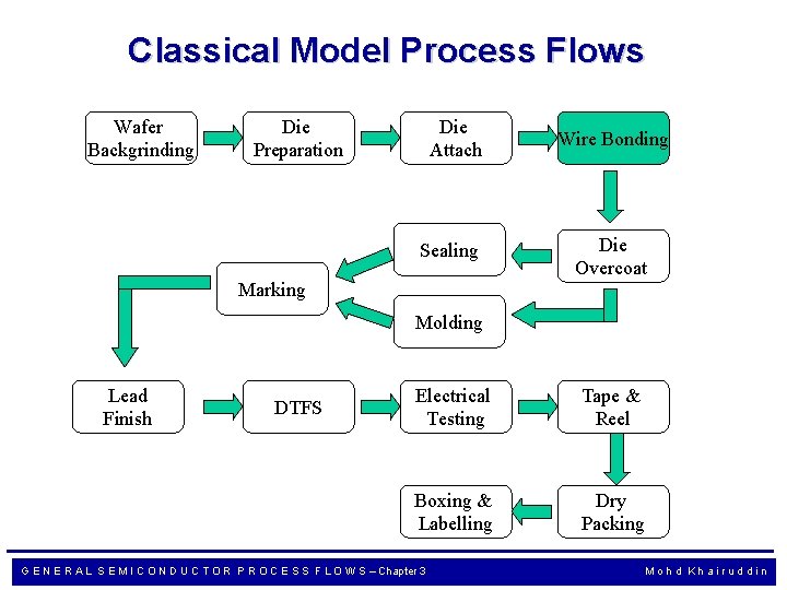
Classical Model Process Flows Wafer Backgrinding Die Preparation Die Attach Sealing Marking Wire Bonding Die Overcoat Molding Lead Finish DTFS Electrical Testing Tape & Reel Boxing & Labelling Dry Packing G E N E R A L S E M I C O N D U C T O R P R O C E S S F L O W S – Chapter 3 Mohd Khairuddin
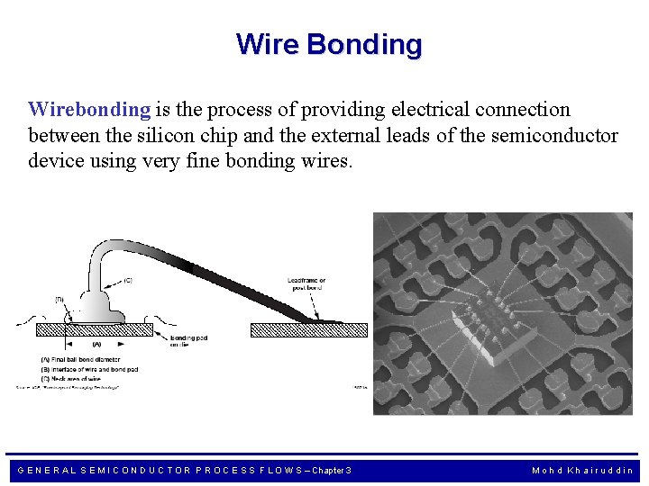
Wire Bonding Wirebonding is the process of providing electrical connection between the silicon chip and the external leads of the semiconductor device using very fine bonding wires. G E N E R A L S E M I C O N D U C T O R P R O C E S S F L O W S – Chapter 3 Mohd Khairuddin
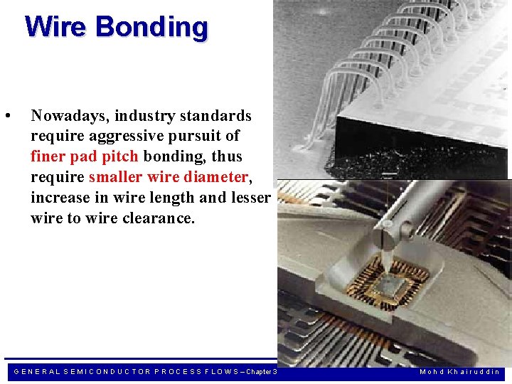
Wire Bonding • Nowadays, industry standards require aggressive pursuit of finer pad pitch bonding, thus require smaller wire diameter, increase in wire length and lesser wire to wire clearance. G E N E R A L S E M I C O N D U C T O R P R O C E S S F L O W S – Chapter 3 Mohd Khairuddin
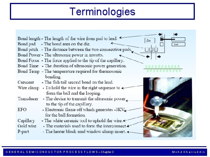
Terminologies G E N E R A L S E M I C O N D U C T O R P R O C E S S F L O W S – Chapter 3 Mohd Khairuddin
Wire Bonding The wire used in wirebonding is usually made either of gold (Au) or aluminum (Al), although Cu wires are starting to gain attention in the semiconductor manufacturing industry. There are three types of wire bonding (thermocompression, ultrasonic and thermosonic ) which can be divided into two common wirebond processes: ball bonding and wedge bonding. There are three basic wire bonding techniques: • • • Thermosonic bonding: utilizes temperature, ultrasonic and low impact force, and ball/ wedge methods. Ultrasonic bonding: utilizes ultrasonic and low impact force, and the wedge/wedge method only. Thermocompression bonding: utilizes high temperature and high impact force, and the ball/wedge method. No ultrasonic is used during bonding. Use in special application such as bonding of Ga. As devices G E N E R A L S E M I C O N D U C T O R P R O C E S S F L O W S – Chapter 3 Mohd Khairuddin
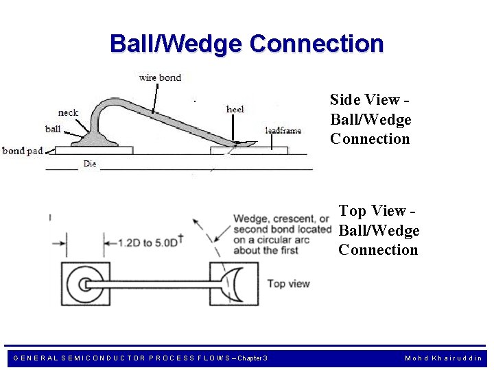
Ball/Wedge Connection Side View Ball/Wedge Connection Top View Ball/Wedge Connection G E N E R A L S E M I C O N D U C T O R P R O C E S S F L O W S – Chapter 3 Mohd Khairuddin
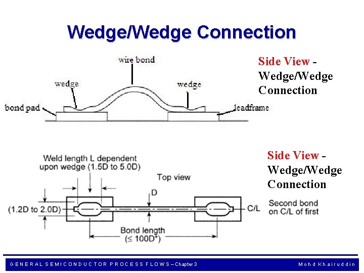
Wedge/Wedge Connection Side View Wedge/Wedge Connection G E N E R A L S E M I C O N D U C T O R P R O C E S S F L O W S – Chapter 3 Mohd Khairuddin
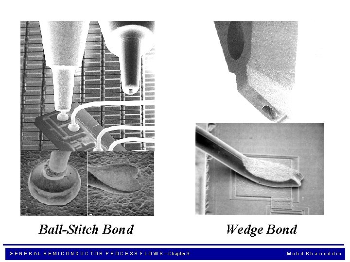
Ball-Stitch Bond G E N E R A L S E M I C O N D U C T O R P R O C E S S F L O W S – Chapter 3 Wedge Bond Mohd Khairuddin
Advantages of Ball/Wedge over Wedge/Wedge 1. The wire can be lead off in any direction from the first ball bond. Thus, it facilitates automation. 2. Wedge/Wedge bonding only has direction to move which means the wire has to travel parallel to the bond foot. Any small deviation from the loop path will create micro crack at the heal and associated reliability problem. 3. The wire from wedge/wedge bonding comes off at a small angle to the substrate and wire can contact to the edge of an active device and short circuit, especially when the second bond is lower than the first bond. G E N E R A L S E M I C O N D U C T O R P R O C E S S F L O W S – Chapter 3 Mohd Khairuddin
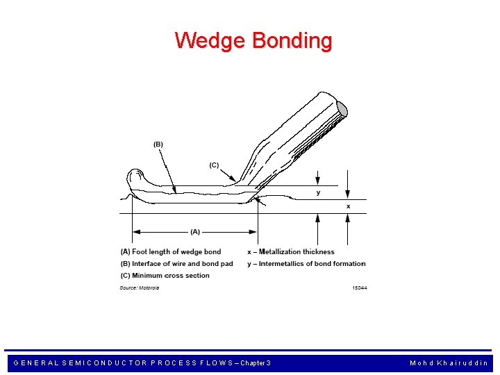
Wedge Bonding G E N E R A L S E M I C O N D U C T O R P R O C E S S F L O W S – Chapter 3 Mohd Khairuddin
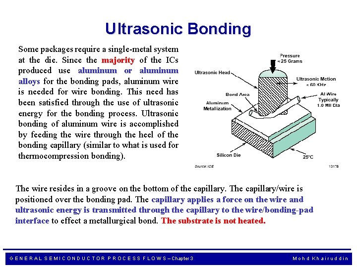
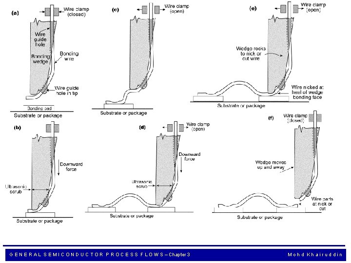
Ultrasonic Bonding Some packages require a single-metal system at the die. Since the majority of the ICs produced use aluminum or aluminum alloys for the bonding pads, aluminum wire is needed for wire bonding. This need has been satisfied through the use of ultrasonic energy for the bonding process. Ultrasonic bonding of aluminum wire is accomplished by feeding the wire through the heel of the bonding capillary (similar to what is used for thermocompression bonding). The wire resides in a groove on the bottom of the capillary. The capillary/wire is positioned over the bonding pad. The capillary applies a force on the wire and ultrasonic energy is transmitted through the capillary to the wire/bonding-pad interface to effect a metallurgical bond. The substrate is not heated. G E N E R A L S E M I C O N D U C T O R P R O C E S S F L O W S – Chapter 3 Mohd Khairuddin
G E N E R A L S E M I C O N D U C T O R P R O C E S S F L O W S – Chapter 3 Mohd Khairuddin
Thermocompression Bonding Thermocompression – In thermocompression bonding both the package substrate or leadframe and bonding capillary are heated. Pure gold or nearly pure gold wire is used. The bonding mechanism positions the wire/capillary assembly over the Al bonding pad on the die. A force is applied to the wire through the capillary. The combination of the applied force and the heat causes the gold/aluminum interface to blend together to form the bond. The capillary feeds out wire as it moves to the post, where a second bond is made in a similar manner. An illustration of thermocompression is almost similar with thermosonic bonding G E N E R A L S E M I C O N D U C T O R P R O C E S S F L O W S – Chapter 3 Mohd Khairuddin
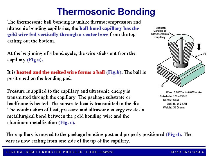
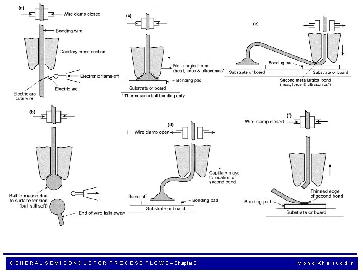
Thermosonic Bonding The thermosonic ball bonding is unlike thermocompression and ultrasonic bonding capillaries, the ball-bond capillary has the gold wire fed vertically through a center bore from the top exiting out the bottom. At the beginning of a bond cycle, the wire sticks out from the capillary (Fig a). It is heated and the melted wire forms a ball (Fig. b). The ball is positioned on the bonding pad. Pressure is applied to the capillary and ultrasonic energy is transmitted through the capillary. The package substrate or leadframe is heated. The substrate heat is transmitted to the die. The combination of heat, pressure and ultrasonic energy creates a metallurgical bond between the gold bonding wire and the aluminum metallization (Fig. c). The capillary is moved to the package bonding post and properly positioned (Fig d). The wire is now exiting from one side of the tip of the capillary. G E N E R A L S E M I C O N D U C T O R P R O C E S S F L O W S – Chapter 3 Mohd Khairuddin
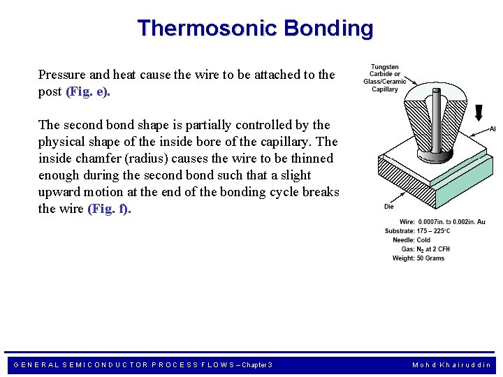
Thermosonic Bonding Pressure and heat cause the wire to be attached to the post (Fig. e). The second bond shape is partially controlled by the physical shape of the inside bore of the capillary. The inside chamfer (radius) causes the wire to be thinned enough during the second bond such that a slight upward motion at the end of the bonding cycle breaks the wire (Fig. f). G E N E R A L S E M I C O N D U C T O R P R O C E S S F L O W S – Chapter 3 Mohd Khairuddin
G E N E R A L S E M I C O N D U C T O R P R O C E S S F L O W S – Chapter 3 Mohd Khairuddin
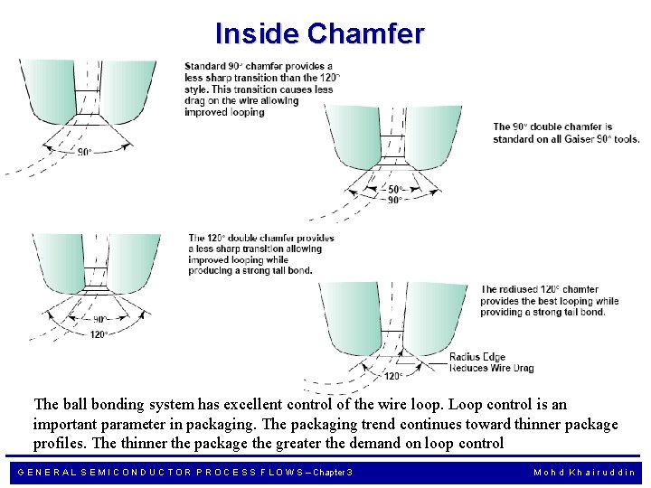
Inside Chamfer The ball bonding system has excellent control of the wire loop. Loop control is an important parameter in packaging. The packaging trend continues toward thinner package profiles. The thinner the package the greater the demand on loop control G E N E R A L S E M I C O N D U C T O R P R O C E S S F L O W S – Chapter 3 Mohd Khairuddin
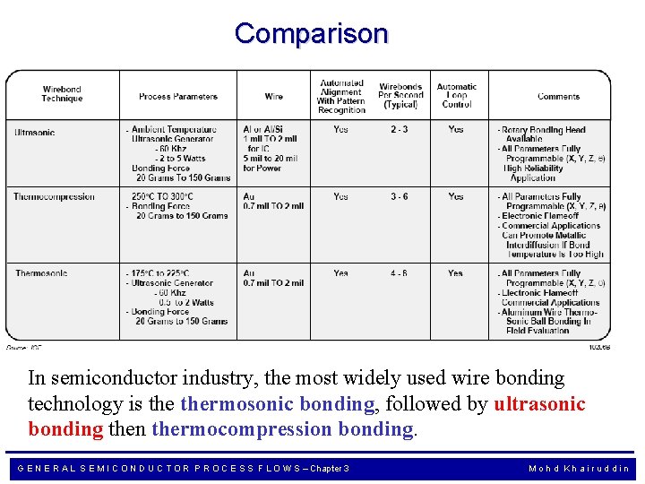
Comparison In semiconductor industry, the most widely used wire bonding technology is thermosonic bonding, followed by ultrasonic bonding then thermocompression bonding. G E N E R A L S E M I C O N D U C T O R P R O C E S S F L O W S – Chapter 3 Mohd Khairuddin
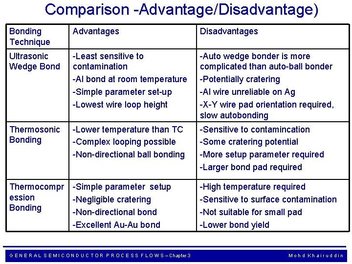
Comparison -Advantage/Disadvantage) Bonding Technique Advantages Disadvantages Ultrasonic Wedge Bond -Least sensitive to contamination -Al bond at room temperature -Simple parameter set-up -Lowest wire loop height -Auto wedge bonder is more complicated than auto-ball bonder -Potentially cratering -Al wire unreliable on Ag -X-Y wire pad orientation required, slow autobonding Thermosonic Bonding -Lower temperature than TC -Complex looping possible -Non-directional ball bonding -Sensitive to contamincation -Some cratering potential -More setup parameter required -Larger bond pad required Thermocompr -Simple parameter setup ession -Negligible cratering Bonding -Non-directional bond -Excellent Au-Au bond G E N E R A L S E M I C O N D U C T O R P R O C E S S F L O W S – Chapter 3 -High temperature required -Sensitive to surface contamination -Not suitable for small pad -Lower bond yield Mohd Khairuddin
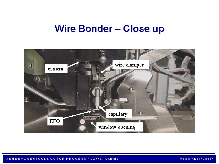
Wire Bonder – Close up camera wire clamper capillary EFO window opening G E N E R A L S E M I C O N D U C T O R P R O C E S S F L O W S – Chapter 3 Mohd Khairuddin
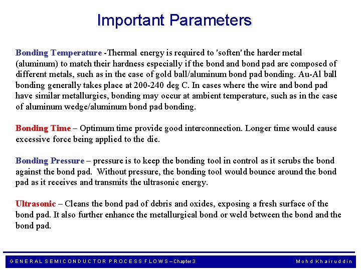
Important Parameters Bonding Temperature -Thermal energy is required to 'soften' the harder metal (aluminum) to match their hardness especially if the bond and bond pad are composed of different metals, such as in the case of gold ball/aluminum bond pad bonding. Au-Al ball bonding generally takes place at 200 -240 deg C. In cases where the wire and bond pad have similar metallurgies, bonding may occur at ambient temperature, such as in the case of aluminum wedge/aluminum bond pad bonding. Bonding Time – Optimum time provide good interconnection. Longer time would cause excessive force being applied to the die. Bonding Pressure – pressure is to keep the bonding tool in control as it scrubs the bond against the bond pad. Without pressure, the bonding tool would bounce around the bond pad as it receives and transmits the ultrasonic energy. Ultrasonic – Cleans the bond pad of debris and oxides, exposing a fresh surface of the bond pad. It also further enhance the metallurgical bond or weld between the bond and the bond pad. G E N E R A L S E M I C O N D U C T O R P R O C E S S F L O W S – Chapter 3 Mohd Khairuddin
Common Wirebond-related Failure Mechanisms Ball Bond Lifting - detachment of the ball bond from the silicon chip; also refers to nonsticking of the ball bond to the bond pad. Common Causes: contamination on the bond pad, incorrect wirebond parameter settings, instability of the die during bonding, bond pad corrosion, excessive bond pad probing, Kirkendall voiding, excessive thermal stress resulting in excessive intermetallic formation, bond pad metallization/barrier metallization lifting, cratering. Wedge Bond Lifting - detachment of the wedge bond from the silicon chip, bonding post, or leadfinger; non-sticking of the wedge bond to the bond pad, post, or leadfinger. Common Causes: contamination on the bond pad or leadfinger, incorrect parameter settings, instability of the die or leadframe during bonding, bond pad or leadfinger corrosion, excessive bond pad probing. Ball Bond Neck Break - breakage of the wire at the neck of the Au ball bond. Common Causes: incorrect wirebond parameter settings, incorrect wire looping, die-topackage delamination, excessive wiresweeping during mold, excessive die overcoat, 'bamboo' grain structure due to excessive thermal treatment G E N E R A L S E M I C O N D U C T O R P R O C E S S F L O W S – Chapter 3 Mohd Khairuddin
Common Wirebond-related Failure Mechanisms Midspan Wire Break - breakage along the span of the wire. Common Causes: wire nicks or damage, wire corrosion, tight wire looping, excessive wiresweeping, electrical overstress Bond-to-Metal Shorting - electrical shorting between the bond a metal line on the die. Common Causes: incorrect wirebond parameter settings, incorrect bond placement, insufficient bond pad-to-metal distance Bond-to-Bond Shorting - electrical shorting between two bonds. Common Causes: incorrect wirebond parameter settings, incorrect bond placement, insufficient bond pad-to-bond pad distance Wedge Bond Heel Break - breakage of the wire at the heel of the Al wedge bond. Common Causes: incorrect wirebond parameter settings, incorrect wire looping, leadfingerto-package delamination, G E N E R A L S E M I C O N D U C T O R P R O C E S S F L O W S – Chapter 3 Mohd Khairuddin
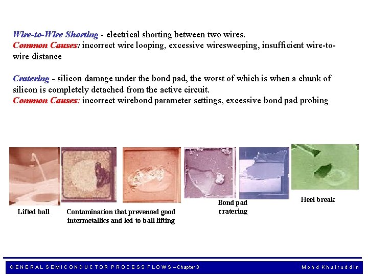
Wire-to-Wire Shorting - electrical shorting between two wires. Common Causes: incorrect wire looping, excessive wiresweeping, insufficient wire-towire distance Cratering - silicon damage under the bond pad, the worst of which is when a chunk of silicon is completely detached from the active circuit. Common Causes: incorrect wirebond parameter settings, excessive bond pad probing Lifted ball Contamination that prevented good intermetallics and led to ball lifting G E N E R A L S E M I C O N D U C T O R P R O C E S S F L O W S – Chapter 3 Bond pad cratering Heel break Mohd Khairuddin
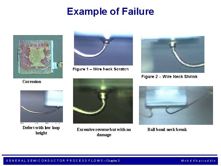
Example of Failure Corrosion Defect with low loop height Excessive reverse but with no damage G E N E R A L S E M I C O N D U C T O R P R O C E S S F L O W S – Chapter 3 Ball bond neck break Mohd Khairuddin
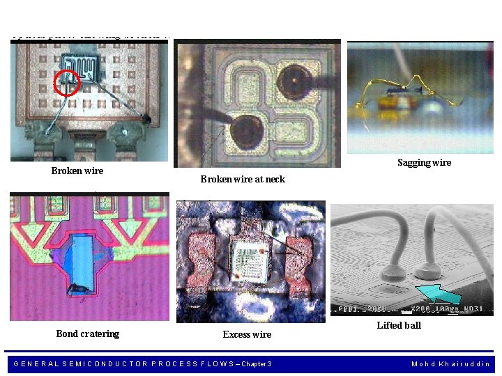
Broken wire Bond cratering Sagging wire Broken wire at neck Excess wire G E N E R A L S E M I C O N D U C T O R P R O C E S S F L O W S – Chapter 3 Lifted ball Mohd Khairuddin
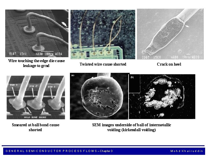
Wire touching the edge die cause leakage to grnd Smeared at ball bond cause shorted Twisted wire cause shorted Crack on heel SEM images underside of ball of intermetallic voiding (kirkendall voiding) G E N E R A L S E M I C O N D U C T O R P R O C E S S F L O W S – Chapter 3 Mohd Khairuddin
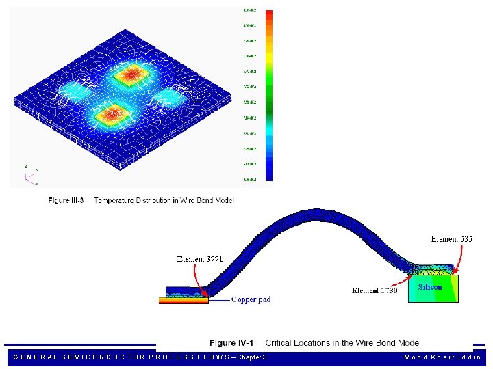
G E N E R A L S E M I C O N D U C T O R P R O C E S S F L O W S – Chapter 3 Mohd Khairuddin
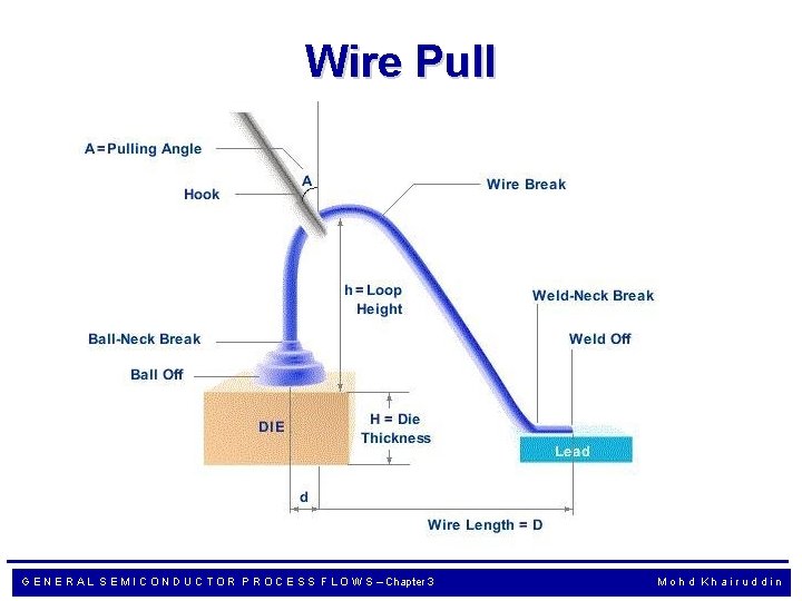
Wire Pull G E N E R A L S E M I C O N D U C T O R P R O C E S S F L O W S – Chapter 3 Mohd Khairuddin
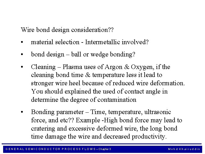
Wire bond design consideration? ? • material selection - Intermetallic involved? • bond design – ball or wedge bonding? • Cleaning – Plasma uses of Argon & Oxygen, if the cleaning bond time & temperature less it lead to stronger wire heel because of reduced wire deformation. You should explained the used of contact angle in determine the degree of contamination • Bonding parameter – Time, temperature, ultrasonic force, and etc? ? Example -High bond force may lead to cratering and excessive deformed wire, the long bond time damage the wire and decreased productivity. G E N E R A L S E M I C O N D U C T O R P R O C E S S F L O W S – Chapter 3 Mohd Khairuddin
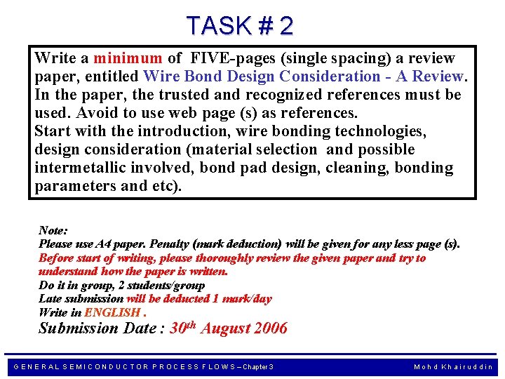
TASK # 2 Write a minimum of FIVE-pages (single spacing) a review paper, entitled Wire Bond Design Consideration - A Review. In the paper, the trusted and recognized references must be used. Avoid to use web page (s) as references. Start with the introduction, wire bonding technologies, design consideration (material selection and possible intermetallic involved, bond pad design, cleaning, bonding parameters and etc). Note: Please use A 4 paper. Penalty (mark deduction) will be given for any less page (s). Before start of writing, please thoroughly review the given paper and try to understand how the paper is written. Do it in group, 2 students/group Late submission will be deducted 1 mark/day Write in ENGLISH. Submission Date : 30 th August 2006 G E N E R A L S E M I C O N D U C T O R P R O C E S S F L O W S – Chapter 3 Mohd Khairuddin
• Introduction – 20 marks • Structure & Flow – 30 marks • Contents – 50 marks G E N E R A L S E M I C O N D U C T O R P R O C E S S F L O W S – Chapter 3 Mohd Khairuddin
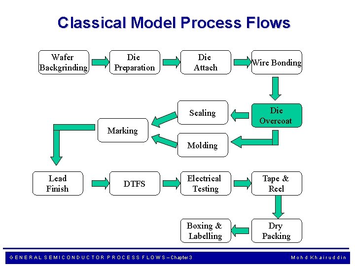
Classical Model Process Flows Wafer Backgrinding Die Preparation Die Attach Sealing Marking Wire Bonding Die Overcoat Molding Lead Finish DTFS Electrical Testing Tape & Reel Boxing & Labelling Dry Packing G E N E R A L S E M I C O N D U C T O R P R O C E S S F L O W S – Chapter 3 Mohd Khairuddin
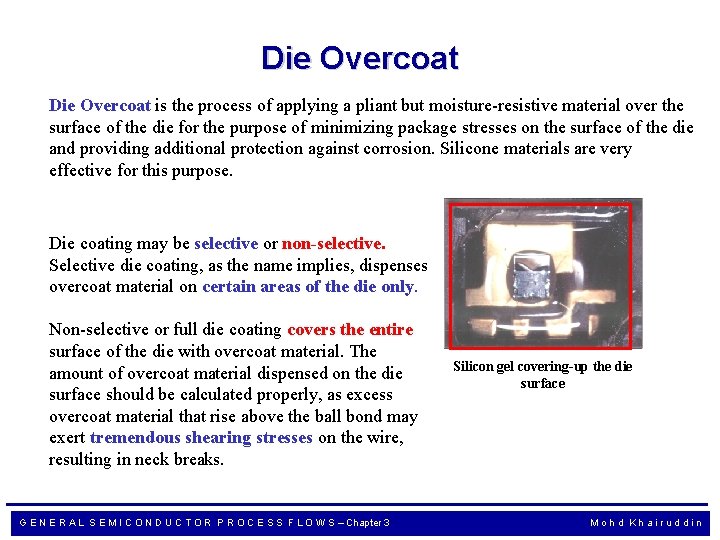
Die Overcoat is the process of applying a pliant but moisture-resistive material over the surface of the die for the purpose of minimizing package stresses on the surface of the die and providing additional protection against corrosion. Silicone materials are very effective for this purpose. Die coating may be selective or non-selective. Selective die coating, as the name implies, dispenses overcoat material on certain areas of the die only. Non-selective or full die coating covers the entire surface of the die with overcoat material. The amount of overcoat material dispensed on the die surface should be calculated properly, as excess overcoat material that rise above the ball bond may exert tremendous shearing stresses on the wire, resulting in neck breaks. G E N E R A L S E M I C O N D U C T O R P R O C E S S F L O W S – Chapter 3 Silicon gel covering-up the die surface Mohd Khairuddin
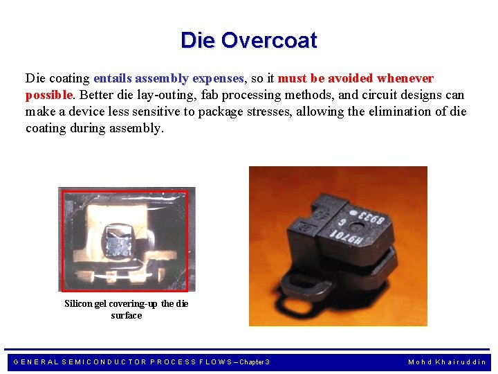
Die Overcoat Die coating entails assembly expenses, so it must be avoided whenever possible. Better die lay-outing, fab processing methods, and circuit designs can make a device less sensitive to package stresses, allowing the elimination of die coating during assembly. Silicon gel covering-up the die surface G E N E R A L S E M I C O N D U C T O R P R O C E S S F L O W S – Chapter 3 Mohd Khairuddin
G E N E R A L S E M I C O N D U C T O R P R O C E S S F L O W S – Chapter 3 Mohd Khairuddin
Common Die Overcoat-related Failure Mechanisms Die Stressing - generation of excessive package stresses on the die which may result in electrical failure; this mechanism is alleviated by die overcoating Die Scratch - inducement of any mechanical damage on the die, as when an operator scratches a die with tweezers due to mishandling. Common Causes: insufficient operator training, disorderly workplace, use of improper tools Die Metallization Smearing - depression or deformation of any metal line on the die surface. Common Causes: dirty or worn-out die attach pick-and-place tool, wafer Mishandling Die Corrosion - corrosion of the metal lines of the die, often due to the presence of corrosive contaminants and moisture on the die surface Neck Breaking - breakage of the bond wire at the ball bond neck. In the context of die coating, it is usually caused by excessive overcoat material which can exert tremendous shearing stresses at the neck. G E N E R A L S E M I C O N D U C T O R P R O C E S S F L O W S – Chapter 3 Mohd Khairuddin
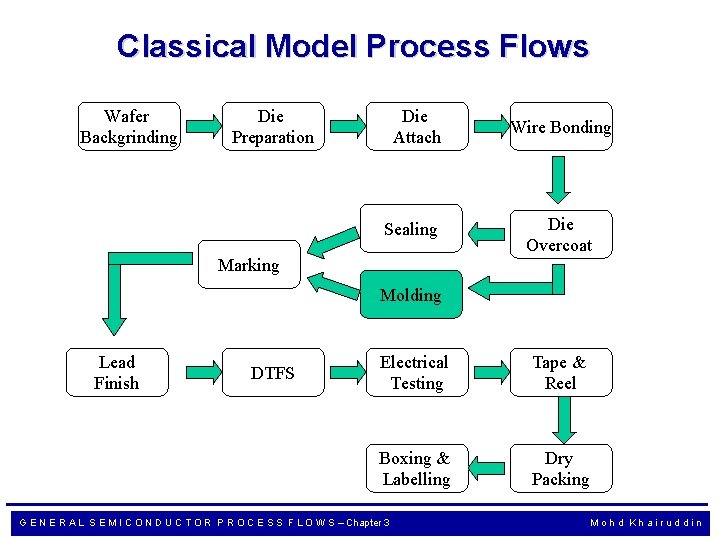
Classical Model Process Flows Wafer Backgrinding Die Preparation Die Attach Sealing Marking Wire Bonding Die Overcoat Molding Lead Finish DTFS Electrical Testing Tape & Reel Boxing & Labelling Dry Packing G E N E R A L S E M I C O N D U C T O R P R O C E S S F L O W S – Chapter 3 Mohd Khairuddin
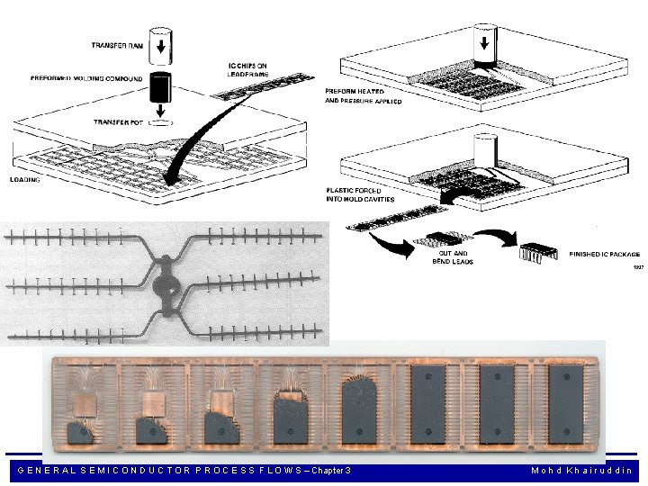
Molding is the process of encapsulating the device in plastic material. Transfer molding is one of the most widely used molding processes in the semiconductor industry because of its capability to mold small parts with complex features. In this process, the molding compound is first preheated prior to its loading into the molding chamber After pre-heating, the molding compound is forced by a hydraulic plunger into the pot where it reaches melting temperature and becomes fluid. The plunger (pelocok) then continues to force the fluid molding compound into the runners of the mold chase. These runners serve as canals (terusan) where the fluid molding compound travels until it reaches the cavities, which contain the leadframes for encapsulation In conventional flow chambers, the cavities are filled up in a 'christmas tree' fashion, i. e. , cavities that are nearer the cull get filled up first G E N E R A L S E M I C O N D U C T O R P R O C E S S F L O W S – Chapter 3 Mohd Khairuddin
G E N E R A L S E M I C O N D U C T O R P R O C E S S F L O W S – Chapter 3 Mohd Khairuddin
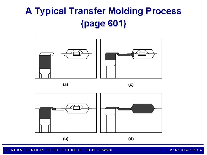
A Typical Transfer Molding Process (page 601) G E N E R A L S E M I C O N D U C T O R P R O C E S S F L O W S – Chapter 3 Mohd Khairuddin
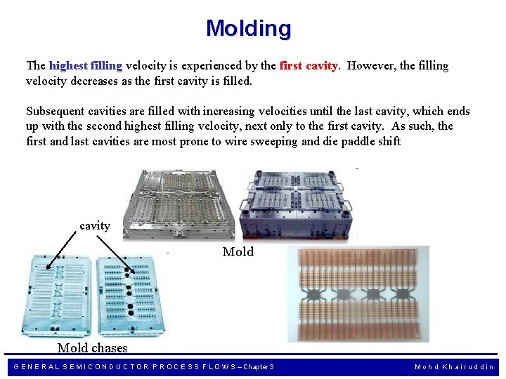
Molding The highest filling velocity is experienced by the first cavity. However, the filling velocity decreases as the first cavity is filled. Subsequent cavities are filled with increasing velocities until the last cavity, which ends up with the second highest filling velocity, next only to the first cavity. As such, the first and last cavities are most prone to wire sweeping and die paddle shift cavity Mold chases G E N E R A L S E M I C O N D U C T O R P R O C E S S F L O W S – Chapter 3 Mohd Khairuddin
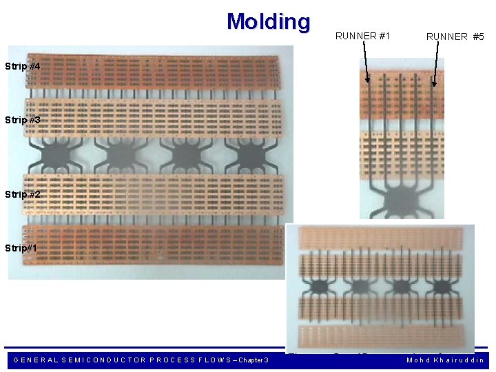
Molding RUNNER #1 RUNNER #5 Strip #4 Strip #3 Strip #2 Strip#1 Cull G E N E R A L S E M I C O N D U C T O R P R O C E S S F L O W S – Chapter 3 Mohd Khairuddin
Common Molding-related Failure Mechanisms Package cracking - occurrence of fracture anywhere in the package; Cause : Fatigue fracture of the encapsulant due to CTE mismatch; these stresses are large enough to cause delamination Package stress - related electrical failure - non-conformance to electrical specifications due to component degradation caused by stresses on the die surface Wire sweeping - swaying or movement of the wires during molding along the direction of mold flow which may result in broken wires or wire shorting. Tends to occur on wires that are perpendicular to flow direction, typically near the gate where polymer enter the mold cavity. Cause : polymer viscosity; local high flow rates; void entrapment; and filler particle collisions with wire Package Voids and Pits - imperfections on the package surface (pits) or body (voids) characterized by vacancies of plastic material Cause: low flow rates, void entrapment. G E N E R A L S E M I C O N D U C T O R P R O C E S S F L O W S – Chapter 3 Mohd Khairuddin
Common Molding-related Failure Mechanisms Package Delamination - any disbonding between the molding compound another material of the package Cause : CTE mismatch between plastic package, leadframe and die. Incomplete Filling - insufficient encapsulation resulting when the molding compound fails to fill up the cavity during molding Cause : contaminant , low adhesion Blistering - appearance of blisters (gelembung) on the package surface Excessive Flashes - presence of unacceptable amounts of plastic on the edges of the package after molding Solder Voids - exposure of any part of the lead base metal resulting when excess flashes that covered the leads during leadfinish are removed Mark Permanence Failure - inability of the entirety of an ink mark to remain on the package G E N E R A L S E M I C O N D U C T O R P R O C E S S F L O W S – Chapter 3 Mohd Khairuddin
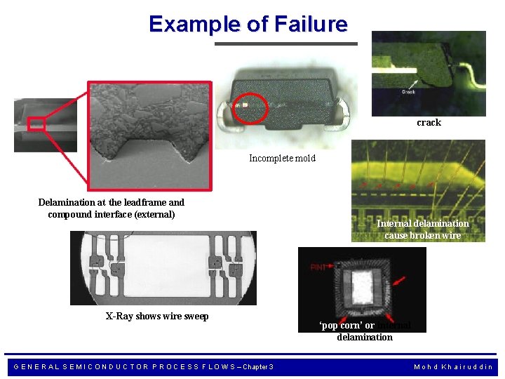
Example of Failure crack Incomplete mold Delamination at the leadframe and compound interface (external) X-Ray shows wire sweep G E N E R A L S E M I C O N D U C T O R P R O C E S S F L O W S – Chapter 3 Internal delamination cause broken wire ‘pop corn’ or internal delamination Mohd Khairuddin
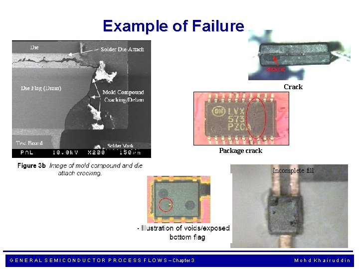
Example of Failure Crack Package crack Incomplete fill G E N E R A L S E M I C O N D U C T O R P R O C E S S F L O W S – Chapter 3 Mohd Khairuddin
Important Parameters a) Molding parameters: Initial transfer position until final transfer position and transfer speed will affect the total transfer time for the mold compound to flow into the mold cavity and later on preload for final compaction. If the transfer speed is fast during the gate entrance, the gold wire will encounter mold compound crushing in and wire will be distorted (wire sweeping problem) due to high viscosity. b) Mold compound : Viscosity, gel time, filler content, filler type and spiral flow are the few elements inside mold compound that we need to consider when checking wire sweep performance. c) Mold design : Runner design for balanced mold flow and gate design location versus the wire position play important roles to have minimum wire sweep percentage G E N E R A L S E M I C O N D U C T O R P R O C E S S F L O W S – Chapter 3 Mohd Khairuddin
Classical Model Process Flows Wafer Backgrinding Die Preparation Die Attach Sealing Marking Wire Bonding Die Overcoat Molding Lead Finish DTFS Electrical Testing Tape & Reel Boxing & Labelling Dry Packing G E N E R A L S E M I C O N D U C T O R P R O C E S S F L O W S – Chapter 3 Mohd Khairuddin
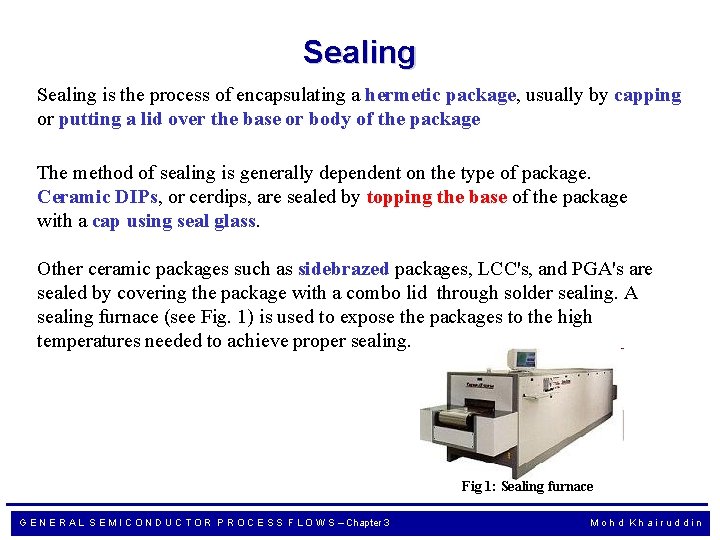
Sealing is the process of encapsulating a hermetic package, usually by capping or putting a lid over the base or body of the package The method of sealing is generally dependent on the type of package. Ceramic DIPs, or cerdips, are sealed by topping the base of the package with a cap using seal glass. Other ceramic packages such as sidebrazed packages, LCC's, and PGA's are sealed by covering the package with a combo lid through solder sealing. A sealing furnace (see Fig. 1) is used to expose the packages to the high temperatures needed to achieve proper sealing. Fig 1: Sealing furnace G E N E R A L S E M I C O N D U C T O R P R O C E S S F L O W S – Chapter 3 Mohd Khairuddin

Types of sealing. Will discuss further in Chapter 7. G E N E R A L S E M I C O N D U C T O R P R O C E S S F L O W S – Chapter 3 Mohd Khairuddin
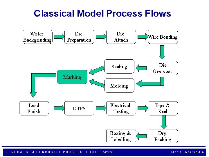
Classical Model Process Flows Wafer Backgrinding Die Preparation Die Attach Sealing Marking Wire Bonding Die Overcoat Molding Lead Finish DTFS Electrical Testing Tape & Reel Boxing & Labelling Dry Packing G E N E R A L S E M I C O N D U C T O R P R O C E S S F L O W S – Chapter 3 Mohd Khairuddin
Marking is the process of putting identification, traceability, and distinguishing marks on the package of an IC. The device name, company logo, date code, and lot id are examples of information commonly marked on the IC's package. Some marks are put on the package during assembly and some marks are put on the package during Test. There are two common marking processes, namely, ink marking and laser marking. G E N E R A L S E M I C O N D U C T O R P R O C E S S F L O W S – Chapter 3 Mohd Khairuddin
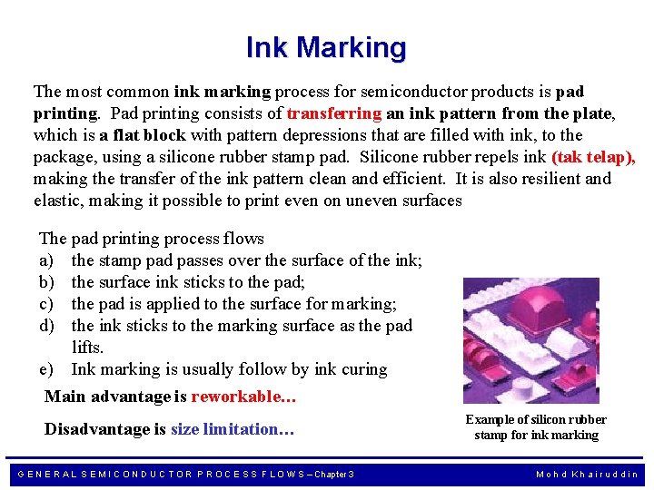
Ink Marking The most common ink marking process for semiconductor products is pad printing. Pad printing consists of transferring an ink pattern from the plate, which is a flat block with pattern depressions that are filled with ink, to the package, using a silicone rubber stamp pad. Silicone rubber repels ink (tak telap), making the transfer of the ink pattern clean and efficient. It is also resilient and elastic, making it possible to print even on uneven surfaces The pad printing process flows a) the stamp pad passes over the surface of the ink; b) the surface ink sticks to the pad; c) the pad is applied to the surface for marking; d) the ink sticks to the marking surface as the pad lifts. e) Ink marking is usually follow by ink curing Main advantage is reworkable… Disadvantage is size limitation… G E N E R A L S E M I C O N D U C T O R P R O C E S S F L O W S – Chapter 3 Example of silicon rubber stamp for ink marking Mohd Khairuddin
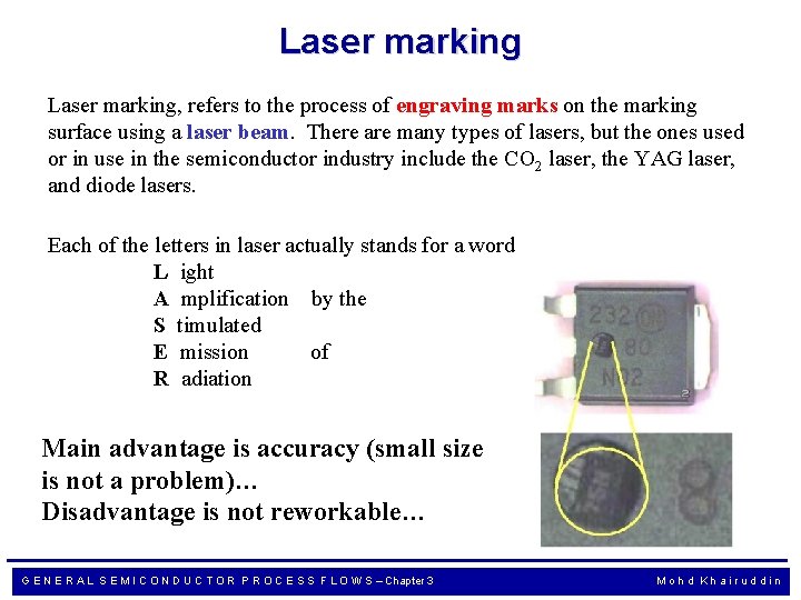
Laser marking, refers to the process of engraving marks on the marking surface using a laser beam. There are many types of lasers, but the ones used or in use in the semiconductor industry include the CO 2 laser, the YAG laser, and diode lasers. Each of the letters in laser actually stands for a word L ight A mplification by the S timulated E mission of R adiation Main advantage is accuracy (small size is not a problem)… Disadvantage is not reworkable… G E N E R A L S E M I C O N D U C T O R P R O C E S S F L O W S – Chapter 3 Mohd Khairuddin
Common Marking-related Failure Mechanisms Missing Mark/Missing Character - absence of or incomplete mark on the package, Mis oriented Mark - improper orientation of the mark on the package Wrong Mark Format - use of incorrect font, positioning, or arrangement for the characters of the mark Mark Permanence Failure - inability of the mark to remain on the package. Can be due to inappropriate ink, use of improperly prepared ink, inadequate ink curing, and marking surface contamination Inadequate Mark Contrast - poor readability of the mark as a result of inadequate color contrast between the mark and package G E N E R A L S E M I C O N D U C T O R P R O C E S S F L O W S – Chapter 3 Mohd Khairuddin
Classical Model Process Flows Wafer Backgrinding Die Preparation Die Attach Sealing Marking Wire Bonding Die Overcoat Molding Lead Finish DTFS Electrical Testing Tape & Reel Boxing & Labelling Dry Packing G E N E R A L S E M I C O N D U C T O R P R O C E S S F L O W S – Chapter 3 Mohd Khairuddin
Lead Finish Leadfinish is the process of applying a coat of metal over the leads of an IC to: 1) protect the leads against corrosion; 2) protect the leads against abrasion; 3) improve the solderability of the leads; 4) improve the appearance of the leads. There are two widely used leadfinish techniques in the semiconductor industry, namely, plating and coating. Further, there are two types of plating, i. e. , pure metal plating such as tin (Sn) plating and alloy plating such as tin/lead (Sn/Pb) plating. G E N E R A L S E M I C O N D U C T O R P R O C E S S F L O W S – Chapter 3 Mohd Khairuddin
Coating is the process of depositing a filler metal (usually solder Sn. Pb) over a surface, achieving metallurgical bonding through surface wetting. The filler metal should have a melting temperature below 315 degrees Celsius for the process to be classified as coating. The driving force for a solder coating process is surface tension, i. e. , wetting of the surface to be coated by the solder must be achieved. A solder diffusion layer grows at the surface-solder interface as solder spreads through the surface during the coating process G E N E R A L S E M I C O N D U C T O R P R O C E S S F L O W S – Chapter 3 Mohd Khairuddin
Plating Tin plating is a form of pure metal electroplating, which is the process of depositing a coating of metal on a surface by passing a current through a conductive medium, or electrolyte. An electroplating system has four (4) components: 1) the cathode, which is the surface to be coated; 2) the anode, which is the source of coating metal; 3) the electrolyte, the aqueous medium through which the metal ions from the anode transfer to the cathode; 4) the power source, which supplies the current or energy needed for the plating process. G E N E R A L S E M I C O N D U C T O R P R O C E S S F L O W S – Chapter 3 Mohd Khairuddin
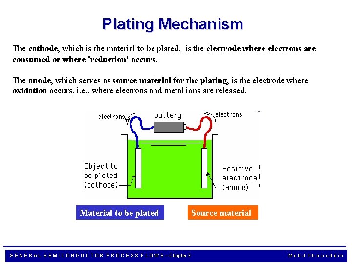
Plating Mechanism The cathode, which is the material to be plated, is the electrode where electrons are consumed or where 'reduction' occurs. The anode, which serves as source material for the plating, is the electrode where oxidation occurs, i. e. , where electrons and metal ions are released. Material to be plated G E N E R A L S E M I C O N D U C T O R P R O C E S S F L O W S – Chapter 3 Source material Mohd Khairuddin
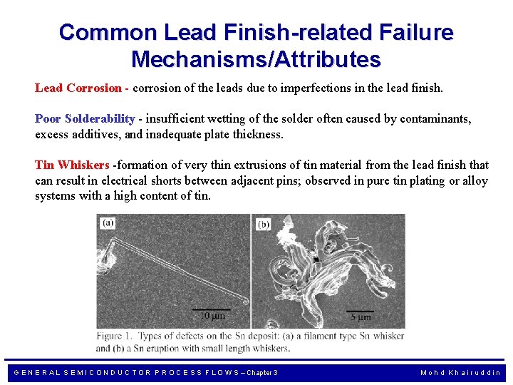
Common Lead Finish-related Failure Mechanisms/Attributes Lead Corrosion - corrosion of the leads due to imperfections in the lead finish. Poor Solderability - insufficient wetting of the solder often caused by contaminants, excess additives, and inadequate plate thickness. Tin Whiskers -formation of very thin extrusions of tin material from the lead finish that can result in electrical shorts between adjacent pins; observed in pure tin plating or alloy systems with a high content of tin. G E N E R A L S E M I C O N D U C T O R P R O C E S S F L O W S – Chapter 3 Mohd Khairuddin
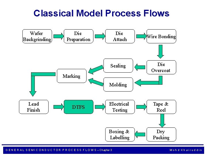
Classical Model Process Flows Wafer Backgrinding Die Preparation Die Attach Sealing Marking Wire Bonding Die Overcoat Molding Lead Finish DTFS Electrical Testing Tape & Reel Boxing & Labelling Dry Packing G E N E R A L S E M I C O N D U C T O R P R O C E S S F L O W S – Chapter 3 Mohd Khairuddin
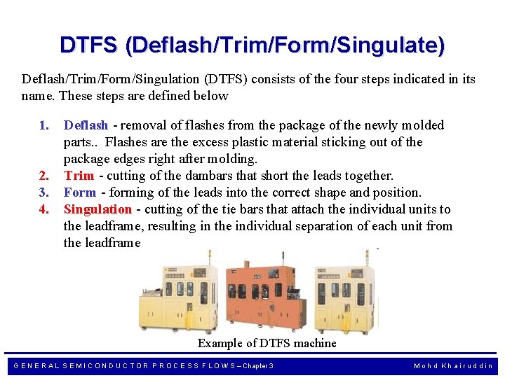
DTFS (Deflash/Trim/Form/Singulate) Deflash/Trim/Form/Singulation (DTFS) consists of the four steps indicated in its name. These steps are defined below 1. 2. 3. 4. Deflash - removal of flashes from the package of the newly molded parts. . Flashes are the excess plastic material sticking out of the package edges right after molding. Trim - cutting of the dambars that short the leads together. Form - forming of the leads into the correct shape and position. Singulation - cutting of the tie bars that attach the individual units to the leadframe, resulting in the individual separation of each unit from the leadframe Example of DTFS machine G E N E R A L S E M I C O N D U C T O R P R O C E S S F L O W S – Chapter 3 Mohd Khairuddin
Common DTFS-Related Failure Mechanisms Package Cracking - occurrence of fracture anywhere in the package, often due to excessive mechanical stresses imparted by the DTFS process to the package. Die Cracking - occurrence of fracture anywhere in the die. In the context of DTFS, die cracking is commonly caused by excessive mechanical stresses imparted by the DTFS process to the package, which may be transmitted to the die. In some cases, the package will withstand these stresses but the die will not. G E N E R A L S E M I C O N D U C T O R P R O C E S S F L O W S – Chapter 3 Mohd Khairuddin
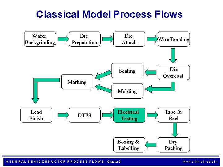
Classical Model Process Flows Wafer Backgrinding Die Preparation Die Attach Sealing Marking Wire Bonding Die Overcoat Molding Lead Finish DTFS Electrical Testing Tape & Reel Boxing & Labelling Dry Packing G E N E R A L S E M I C O N D U C T O R P R O C E S S F L O W S – Chapter 3 Mohd Khairuddin
Electrical Testing Electrical testing is the identification and segregation of electrical failures from a population of devices. An electrical failure is any unit that does not meet the electrical specifications defined for the device. Electrical testing consists of providing a series of electrical excitation (force) to the device under test (DUT) and measuring the response of the DUT. For every set of electrical stimuli (response), the measured response is compared to the expected response, which is usually defined in terms of a lower and an upper limit. Any DUT that exhibits a response outside of the expected range of response is considered a failure. G E N E R A L S E M I C O N D U C T O R P R O C E S S F L O W S – Chapter 3 Mohd Khairuddin
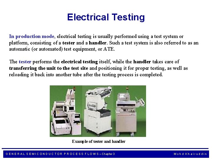
Electrical Testing In production mode, electrical testing is usually performed using a test system or platform, consisting of a tester and a handler. Such a test system is also referred to as an automatic (or automated) test equipment, or ATE. The tester performs the electrical testing itself, while the handler takes care of transferring the unit to the test site and positioning it for proper testing, as well as reloading it back into another tube after the testing process is completed. Example of tester and handler G E N E R A L S E M I C O N D U C T O R P R O C E S S F L O W S – Chapter 3 Mohd Khairuddin
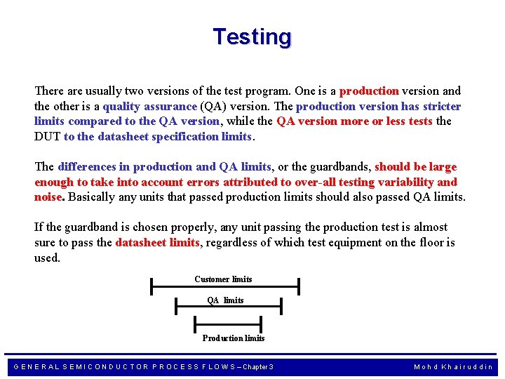
Testing There are usually two versions of the test program. One is a production version and the other is a quality assurance (QA) version. The production version has stricter limits compared to the QA version, while the QA version more or less tests the DUT to the datasheet specification limits. The differences in production and QA limits, or the guardbands, should be large enough to take into account errors attributed to over-all testing variability and noise. Basically any units that passed production limits should also passed QA limits. If the guardband is chosen properly, any unit passing the production test is almost sure to pass the datasheet limits, regardless of which test equipment on the floor is used. Customer limits QA limits Production limits G E N E R A L S E M I C O N D U C T O R P R O C E S S F L O W S – Chapter 3 Mohd Khairuddin
Strip Testing refers to the process wherein semiconductor devices are electrically tested while they are still in their lead frame strips, i. e. , before they are singulated into individual units. Prior to testing, however, the devices in the strip have already undergone the lead trimming process for electrical isolation of their leads. G E N E R A L S E M I C O N D U C T O R P R O C E S S F L O W S – Chapter 3 Mohd Khairuddin
Advantages of Strip Testing • • • reduced cost of test primarily from high degree of parallelism; reduced cycle time from testing in line with assembly; consistently higher yields than singulated test (better contact methodology); higher quality from reduced handling (reduced bent leads); faster time for test development; part traceability to assembly; high strip density (up to 400 devices per strip); reduced floor space; better equipment utilization; significant reduction in test capital expenditures; immediate feedback to assembly. G E N E R A L S E M I C O N D U C T O R P R O C E S S F L O W S – Chapter 3 Mohd Khairuddin
Disadvantages of strip testing • • • It requires heavy reengineering of existing lines for its effective adaptation. Assembly-test integration loses some of the flexibility offered by having both processes independent of each other. Difficulty of retesting or rescreening fall-outs from an initial round of electrical testing Strip retesting, the entire strip will have to go through the strip test process again, thus the good units in the strip get an extra 'handling' that they no longer need, potentially affecting their quality. The units expose to potentially damaged and cause failure after electrical that was due to the number of critical manufacturing steps that the units still need to undergo after they've been subjected to final test Strict process evaluations and qualifications is necessary prior implementation…. . G E N E R A L S E M I C O N D U C T O R P R O C E S S F L O W S – Chapter 3 Mohd Khairuddin
Classical Model Process Flows Wafer Backgrinding Die Preparation Die Attach Sealing Marking Wire Bonding Die Overcoat Molding Lead Finish DTFS Electrical Testing Tape & Reel Boxing & Labelling Dry Packing G E N E R A L S E M I C O N D U C T O R P R O C E S S F L O W S – Chapter 3 Mohd Khairuddin
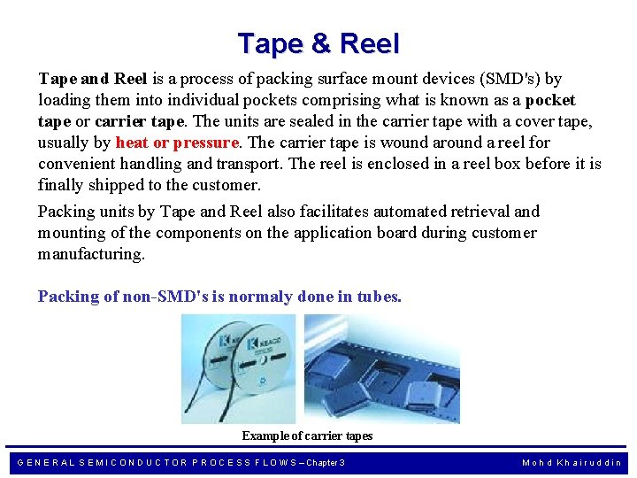
Tape & Reel Tape and Reel is a process of packing surface mount devices (SMD's) by loading them into individual pockets comprising what is known as a pocket tape or carrier tape. The units are sealed in the carrier tape with a cover tape, usually by heat or pressure. The carrier tape is wound around a reel for convenient handling and transport. The reel is enclosed in a reel box before it is finally shipped to the customer. Packing units by Tape and Reel also facilitates automated retrieval and mounting of the components on the application board during customer manufacturing. Packing of non-SMD's is normaly done in tubes. Example of carrier tapes G E N E R A L S E M I C O N D U C T O R P R O C E S S F L O W S – Chapter 3 Mohd Khairuddin
Tape & Reel Requirements The physical and electrical properties of the tape and reel materials used are important to prevent loading/unloading problems and ESD failures. For instance, the materials used in the carrier tape, cover tape, and even reels should be antistatic, if not static dissipative. The ability of these materials to withstand severe environmental conditions (temperature and humidity) for a predefined duration must also be considered. Peel back strength, which is the force needed to peel open the cover tape, must also meet a lower and an upper limit. Depending on the width of the carrier tape, the peel back strength requirement may be as low as a few grams to more than a hundred grams. Peel back strength testing is often done at room temperature, with the pulling action performed at a predefined angle and peel-off speed. G E N E R A L S E M I C O N D U C T O R P R O C E S S F L O W S – Chapter 3 Mohd Khairuddin
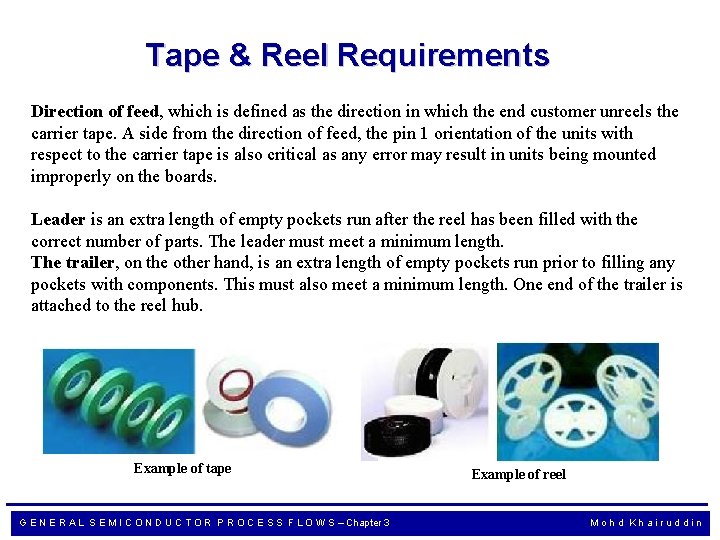
Tape & Reel Requirements Direction of feed, which is defined as the direction in which the end customer unreels the carrier tape. A side from the direction of feed, the pin 1 orientation of the units with respect to the carrier tape is also critical as any error may result in units being mounted improperly on the boards. Leader is an extra length of empty pockets run after the reel has been filled with the correct number of parts. The leader must meet a minimum length. The trailer, on the other hand, is an extra length of empty pockets run prior to filling any pockets with components. This must also meet a minimum length. One end of the trailer is attached to the reel hub. Example of tape G E N E R A L S E M I C O N D U C T O R P R O C E S S F L O W S – Chapter 3 Example of reel Mohd Khairuddin
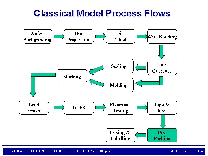
Classical Model Process Flows Wafer Backgrinding Die Preparation Die Attach Sealing Marking Wire Bonding Die Overcoat Molding Lead Finish DTFS Electrical Testing Tape & Reel Boxing & Labelling Dry Packing G E N E R A L S E M I C O N D U C T O R P R O C E S S F L O W S – Chapter 3 Mohd Khairuddin
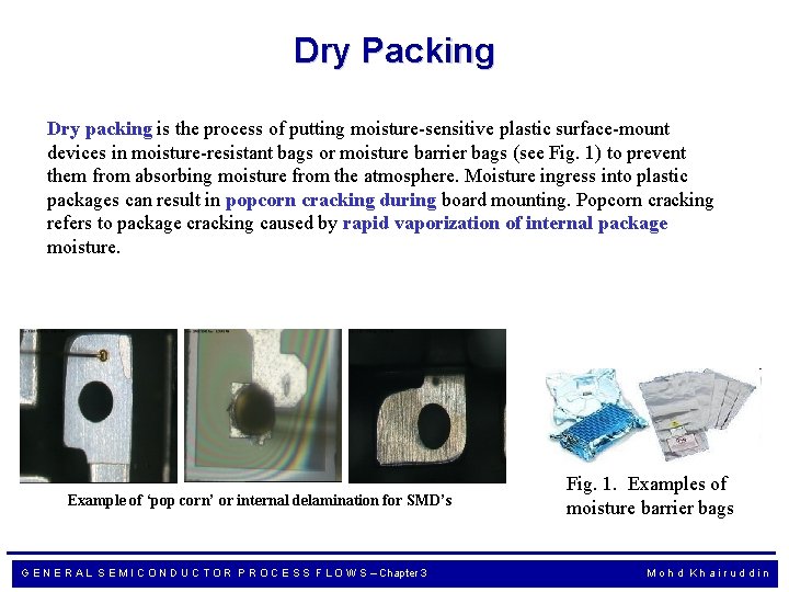
Dry Packing Dry packing is the process of putting moisture-sensitive plastic surface-mount devices in moisture-resistant bags or moisture barrier bags (see Fig. 1) to prevent them from absorbing moisture from the atmosphere. Moisture ingress into plastic packages can result in popcorn cracking during board mounting. Popcorn cracking refers to package cracking caused by rapid vaporization of internal package moisture. Example of ‘pop corn’ or internal delamination for SMD’s G E N E R A L S E M I C O N D U C T O R P R O C E S S F L O W S – Chapter 3 Fig. 1. Examples of moisture barrier bags Mohd Khairuddin
IPC/JEDEC Moisture Sensitivity Levels (MSL) Different packages have different levels of moisture sensitivity. The higher the amount of moisture inside a package, the higher thermomechanical stresses inside the package during board mounting will be. These stresses are brought about by the rapid vaporization of the trapped moisture, and can be large enough to fracture the package when the device is subjected to sudden, elevated temperature, such as during board mounting. Package cracking due to such moisture-induced stresses is known as popcorn cracking. In general, surface-mount devices (SMD's) are more prone to popcorn cracking because: 1) they are thinner and therefore has lower fracture strength; 2) they absorb and retain moisture more easily; and 3) SMD board mounting also subjects the molding compound to the high temperature experienced by the leads. G E N E R A L S E M I C O N D U C T O R P R O C E S S F L O W S – Chapter 3 Mohd Khairuddin
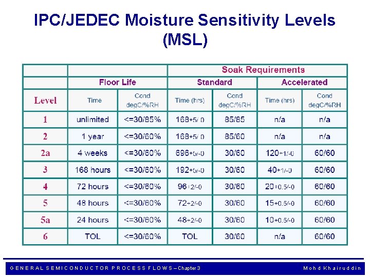
IPC/JEDEC Moisture Sensitivity Levels (MSL) G E N E R A L S E M I C O N D U C T O R P R O C E S S F L O W S – Chapter 3 Mohd Khairuddin
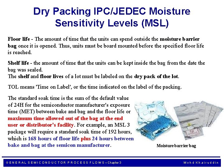
Dry Packing IPC/JEDEC Moisture Sensitivity Levels (MSL) Floor life - The amount of time that the units can spend outside the moisture barrier bag once it is opened. Thus, units must be board mounted before the specified floor life is reached. Shelf life - the amount of time that the units can be kept inside the bag from the date the bag was sealed. The shelf and floor lives of a lot must be labeled on the dry pack of the lot. TOL means 'Time on Label', or the time indicated on the label of the packing. The standard soak time is the sum of the default value of 24 H for the semiconductor manufacturer's exposure time (MET) between bake and bag and the floor life or maximum time allowed out of the bag at the end user or distributor's facility. For example, an MSL 3 package will require a standard soak time of 192 hours, which is 168 hours of floor life plus 24 hours between bake and bag at the semicon manufacturer. G E N E R A L S E M I C O N D U C T O R P R O C E S S F L O W S – Chapter 3 Moisture barrier bag Mohd Khairuddin
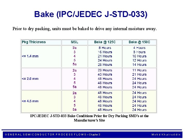
Bake (IPC/JEDEC J-STD-033) Prior to dry packing, units must be baked to drive any internal moisture away. IPC/JEDEC J-STD-033 Bake Conditions Prior for Dry Packing SMD's at the Manufacturer's Site G E N E R A L S E M I C O N D U C T O R P R O C E S S F L O W S – Chapter 3 Mohd Khairuddin
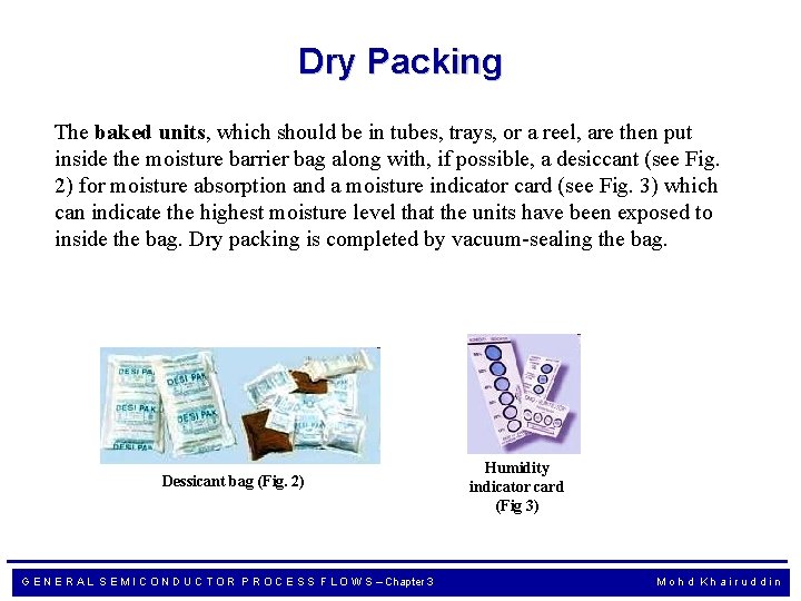
Dry Packing The baked units, which should be in tubes, trays, or a reel, are then put inside the moisture barrier bag along with, if possible, a desiccant (see Fig. 2) for moisture absorption and a moisture indicator card (see Fig. 3) which can indicate the highest moisture level that the units have been exposed to inside the bag. Dry packing is completed by vacuum-sealing the bag. Dessicant bag (Fig. 2) G E N E R A L S E M I C O N D U C T O R P R O C E S S F L O W S – Chapter 3 Humidity indicator card (Fig 3) Mohd Khairuddin
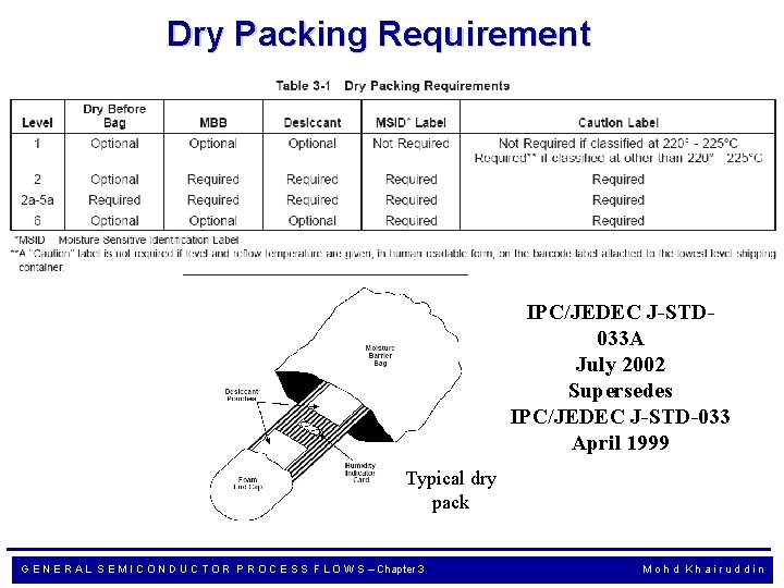
Dry Packing Requirement IPC/JEDEC J-STD 033 A July 2002 Supersedes IPC/JEDEC J-STD-033 April 1999 Typical dry pack G E N E R A L S E M I C O N D U C T O R P R O C E S S F L O W S – Chapter 3 Mohd Khairuddin
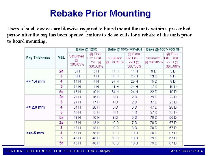
Rebake Prior Mounting Users of such devices are likewise required to board mount the units within a prescribed period after the bag has been opened. Failure to do so calls for a rebake of the units prior to board mounting. G E N E R A L S E M I C O N D U C T O R P R O C E S S F L O W S – Chapter 3 Mohd Khairuddin
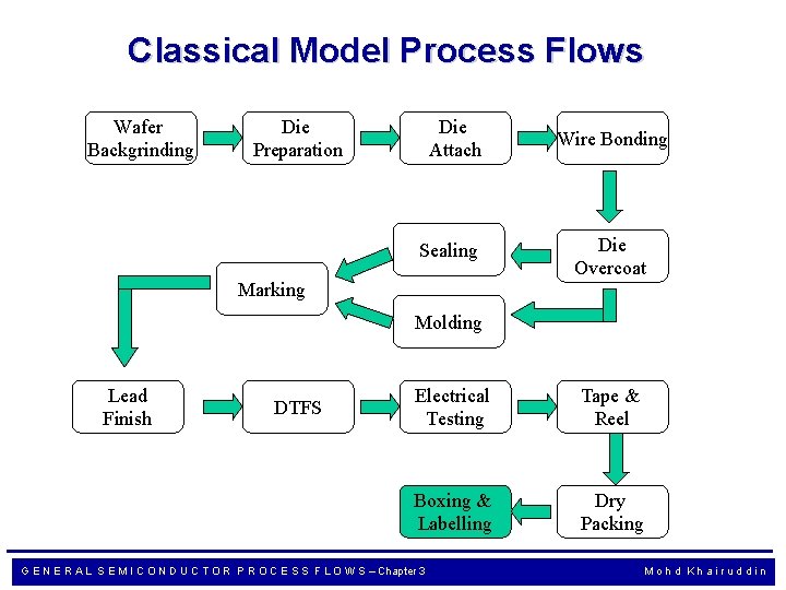
Classical Model Process Flows Wafer Backgrinding Die Preparation Die Attach Sealing Marking Wire Bonding Die Overcoat Molding Lead Finish DTFS Electrical Testing Tape & Reel Boxing & Labelling Dry Packing G E N E R A L S E M I C O N D U C T O R P R O C E S S F L O W S – Chapter 3 Mohd Khairuddin
Boxing and Labelling Boxing and Labeling, is the process of packing the lot (a group of devices built under a single process cycle as one batch) in its final box and attaching the required lot identification labels for storage in the finished goods warehouse or shipment to the customer. Boxing and labeling procedures and materials differ from company to company, customer to customer, or even package to package. For the most part though, units either go into tubes or reels. For units in tubes, the tubes are often simply arranged neatly inside boxes that are just a little longer than the tubes. The number of tubes put in the box depends on the size of the box and tubes. The tubes are topped with enough dunnage paper to keep them from moving around before the box is sealed. Boxing of units in reels is even simpler, with each reel simply put inside a reel box. All required labels are put on the reel prior to keeping it in the reel box. Boxes are generally sealed across the flaps with paper gum tape. The necessary labels are put on the boxes prior to storage or shipment. Labels often contain the product name, the lot quantity, the lot ID, and the country of assembly. G E N E R A L S E M I C O N D U C T O R P R O C E S S F L O W S – Chapter 3 Mohd Khairuddin
TASK # 2 Write a minimum of THREE-pages (single spacing) a term paper (what other people has done). The TITLE should reflect one of the processes in this chapter (ex. Ball Stitch on ball in wire bonding, delamination in molding process or etc). In the paper, the trusted and recognized references must be used. Avoid to use web page (s) as references. Start with the Abstract, introduction, technologies, conclusion (your own word) and references. Note: The chosen topic must be agreed and discussed with me to avoid mark deduction. Please use A 4 paper. Penalty (mark deduction) will be given for any less page (s). Before start of writing, please thoroughly review the given paper and try to understand how the paper is written. Do it in group, 2 students/group Late submission will be deducted 1 mark/day Write in ENGLISH and DON’T blindly copy Submission Date : 25 August 2008 G E N E R A L S E M I C O N D U C T O R P R O C E S S F L O W S – Chapter 3 Mohd Khairuddin
TASK # 2 Topic for consideration: Intermetallic involved in Au-Al metallization Delamination in plastic packaging Small diameter of wire bonding for fine pitch Wafer thinning technologies Previous study on Plasma Cleaning prior to wire bonding process. And etc. . G E N E R A L S E M I C O N D U C T O R P R O C E S S F L O W S – Chapter 3 Mohd Khairuddin
• • Abstract/Introduction – 20 marks Contents/Technologies – 50 marks Conclusion/Finishing – 20 marks Structure & Flow – 10 marks G E N E R A L S E M I C O N D U C T O R P R O C E S S F L O W S – Chapter 3 Mohd Khairuddin

END…Chapter 3…. G E N E R A L S E M I C O N D U C T O R P R O C E S S F L O W S – Chapter 3 Mohd Khairuddin
- Slides: 130