General Purpose IO ARM University Program Copyright ARM


- Slides: 24

General Purpose I/O ARM University Program Copyright © ARM Ltd 2013 1

Overview § How do we make a program light up LEDs in response to a switch? § GPIO § § § Port Circuitry Control Registers Accessing Hardware Registers in C Clocking and Muxing Circuit Interfacing § § § Basic Concepts Inputs Outputs Additional Configuration ARM University Program Copyright © ARM Ltd 2013 2

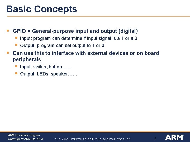
Basic Concepts § GPIO = General-purpose input and output (digital) § § § Input: program can determine if input signal is a 1 or a 0 Output: program can set output to 1 or 0 Can use this to interface with external devices or on board peripherals § § Input: switch, button…… Output: LEDs, speaker…… ARM University Program Copyright © ARM Ltd 2013 3

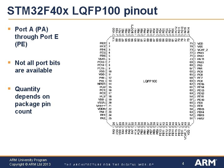
STM 32 F 40 x LQFP 100 pinout § Port A (PA) through Port E (PE) § Not all port bits are available § Quantity depends on package pin count ARM University Program Copyright © ARM Ltd 2013 4

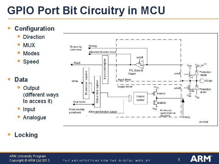
GPIO Port Bit Circuitry in MCU § Configuration § § § Modes Speed Data § § Direction MUX Output (different ways to access it) Input Analogue Locking ARM University Program Copyright © ARM Ltd 2013 5

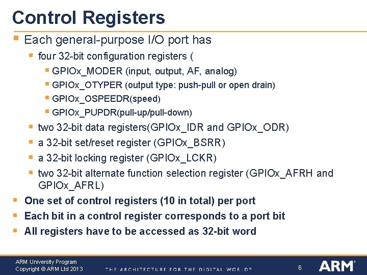
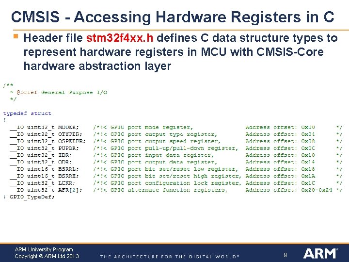
Control Registers § Each general-purpose I/O port has § four 32 -bit configuration registers ( § GPIOx_MODER (input, output, AF, analog) § GPIOx_OTYPER (output type: push-pull or open drain) § GPIOx_OSPEEDR(speed) § GPIOx_PUPDR(pull-up/pull-down) § § § § two 32 -bit data registers(GPIOx_IDR and GPIOx_ODR) a 32 -bit set/reset register (GPIOx_BSRR) a 32 -bit locking register (GPIOx_LCKR) two 32 -bit alternate function selection register (GPIOx_AFRH and GPIOx_AFRL) One set of control registers (10 in total) per port Each bit in a control register corresponds to a port bit All registers have to be accessed as 32 -bit word ARM University Program Copyright © ARM Ltd 2013 6

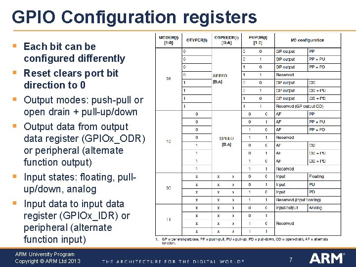
GPIO Configuration registers § Each bit can be configured differently § Reset clears port bit direction to 0 Output modes: push-pull or open drain + pull-up/down Output data from output data register (GPIOx_ODR) or peripheral (alternate function output) Input states: floating, pullup/down, analog Input data to input data register (GPIOx_IDR) or peripheral (alternate function input) § § ARM University Program Copyright © ARM Ltd 2013 7

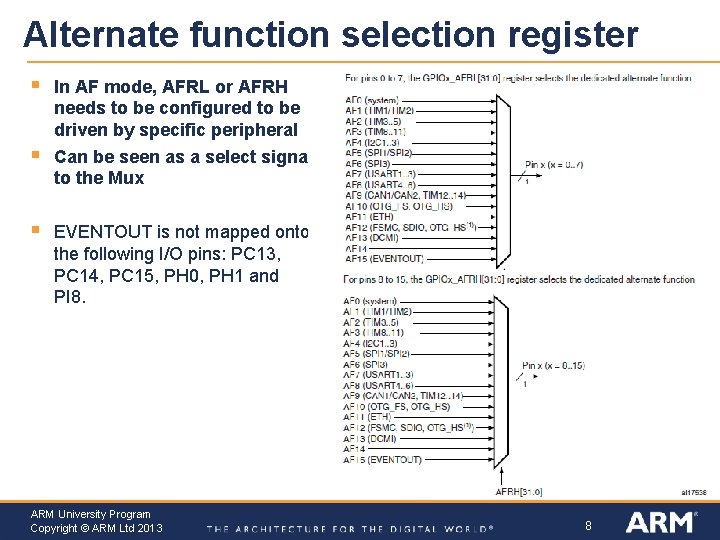
Alternate function selection register § In AF mode, AFRL or AFRH needs to be configured to be driven by specific peripheral § Can be seen as a select signal to the Mux § EVENTOUT is not mapped onto the following I/O pins: PC 13, PC 14, PC 15, PH 0, PH 1 and PI 8. ARM University Program Copyright © ARM Ltd 2013 8

CMSIS - Accessing Hardware Registers in C § Header file stm 32 f 4 xx. h defines C data structure types to represent hardware registers in MCU with CMSIS-Core hardware abstraction layer ARM University Program Copyright © ARM Ltd 2013 9

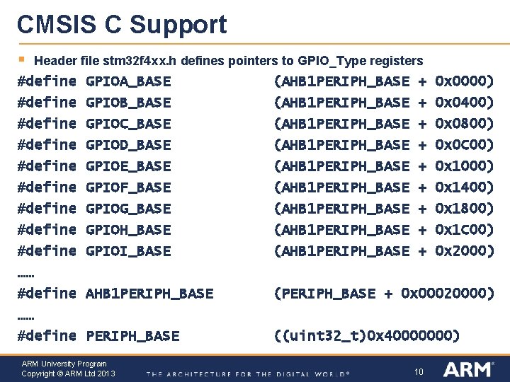
CMSIS C Support § Header file stm 32 f 4 xx. h defines pointers to GPIO_Type registers #define GPIOA_BASE #define GPIOB_BASE #define GPIOC_BASE (AHB 1 PERIPH_BASE + 0 x 0000) (AHB 1 PERIPH_BASE + 0 x 0400) (AHB 1 PERIPH_BASE + 0 x 0800) #define #define …… #define GPIOD_BASE GPIOE_BASE GPIOF_BASE GPIOG_BASE GPIOH_BASE GPIOI_BASE (AHB 1 PERIPH_BASE (AHB 1 PERIPH_BASE (PERIPH_BASE + 0 x 00020000) PERIPH_BASE ((uint 32_t)0 x 40000000) ARM University Program Copyright © ARM Ltd 2013 + + + 10 0 x 0 C 00) 0 x 1000) 0 x 1400) 0 x 1800) 0 x 1 C 00) 0 x 2000)

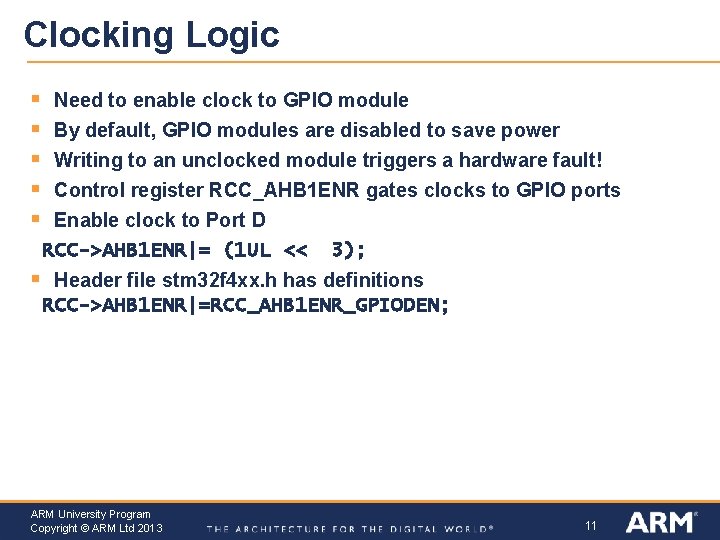
Clocking Logic § § § Need to enable clock to GPIO module By default, GPIO modules are disabled to save power Writing to an unclocked module triggers a hardware fault! Control register RCC_AHB 1 ENR gates clocks to GPIO ports Enable clock to Port D RCC->AHB 1 ENR|= (1 UL << 3); Header file stm 32 f 4 xx. h has definitions RCC->AHB 1 ENR|=RCC_AHB 1 ENR_GPIODEN; ARM University Program Copyright © ARM Ltd 2013 11

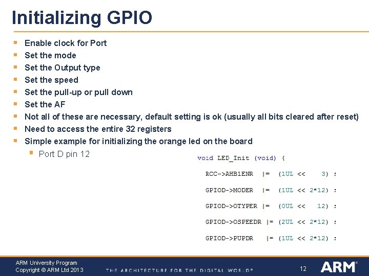
Initializing GPIO § § § § § Enable clock for Port Set the mode Set the Output type Set the speed Set the pull-up or pull down Set the AF Not all of these are necessary, default setting is ok (usually all bits cleared after reset) Need to access the entire 32 registers Simple example for initializing the orange led on the board § Port D pin 12 ARM University Program Copyright © ARM Ltd 2013 12

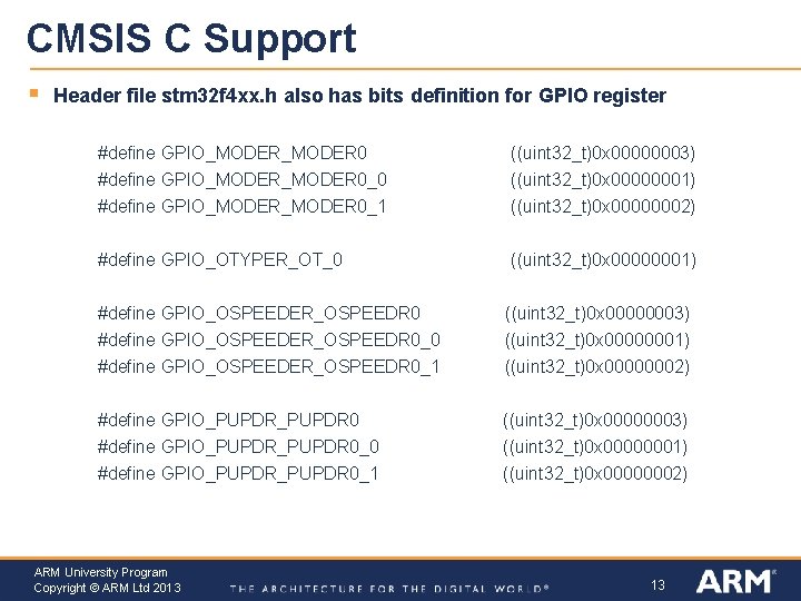
CMSIS C Support § Header file stm 32 f 4 xx. h also has bits definition for GPIO register #define GPIO_MODER 0 ((uint 32_t)0 x 00000003) #define GPIO_MODER 0_0 ((uint 32_t)0 x 00000001) #define GPIO_MODER 0_1 ((uint 32_t)0 x 00000002) #define GPIO_OTYPER_OT_0 ((uint 32_t)0 x 00000001) #define GPIO_OSPEEDER_OSPEEDR 0_0 #define GPIO_OSPEEDER_OSPEEDR 0_1 ((uint 32_t)0 x 00000003) ((uint 32_t)0 x 00000001) ((uint 32_t)0 x 00000002) #define GPIO_PUPDR_PUPDR 0_0 #define GPIO_PUPDR 0_1 ((uint 32_t)0 x 00000003) ((uint 32_t)0 x 00000001) ((uint 32_t)0 x 00000002) ARM University Program Copyright © ARM Ltd 2013 13

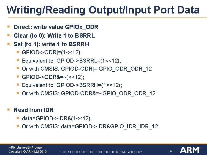
Writing/Reading Output/Input Port Data § § § Direct: write value GPIOx_ODR Clear (to 0): Write 1 to BSRRL Set (to 1): write 1 to BSRRH § § § § GPIOD->ODR|=(1<<12); Equivalent to: GPIOD->BSRRL=(1<<12); Or with CMSIS: GPIOD-ODR|= GPIO_ODR_12 GPIOD->ODR&=~(<<12); Equivalent to: GPIOD->BSRRH=(1<<12); Or with CMSIS: GPIOD-ODR&=~GPIO_ODR_12 Read from IDR § § data=GPIOD->IDR&(1<<12) Or with CMSIS: data=GPIOD->IDR&GPIO_IDR_12 ARM University Program Copyright © ARM Ltd 2013 14

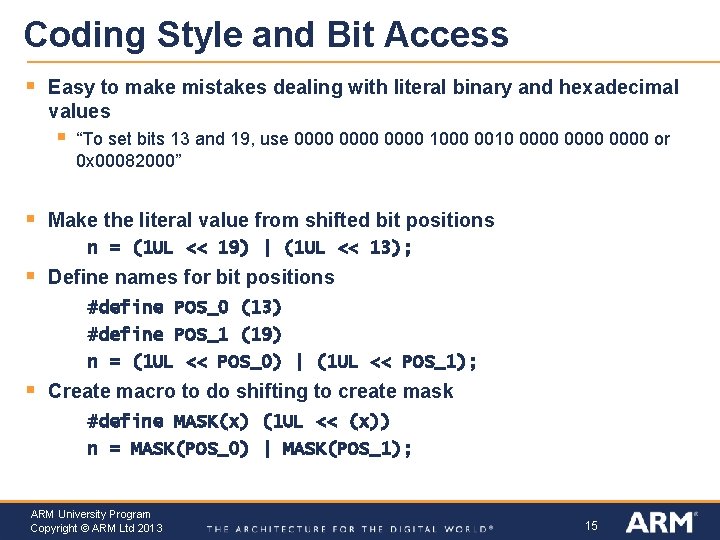
Coding Style and Bit Access § Easy to make mistakes dealing with literal binary and hexadecimal values § § “To set bits 13 and 19, use 0000 1000 0010 0000 or 0 x 00082000” Make the literal value from shifted bit positions n = (1 UL << 19) | (1 UL << 13); § Define names for bit positions #define POS_0 (13) #define POS_1 (19) n = (1 UL << POS_0) | (1 UL << POS_1); § Create macro to do shifting to create mask #define MASK(x) (1 UL << (x)) n = MASK(POS_0) | MASK(POS_1); ARM University Program Copyright © ARM Ltd 2013 15

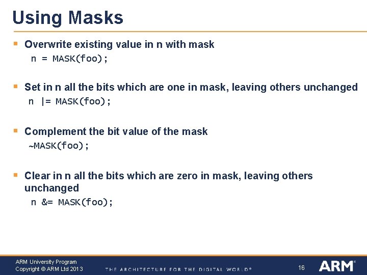
Using Masks § Overwrite existing value in n with mask n = MASK(foo); § Set in n all the bits which are one in mask, leaving others unchanged n |= MASK(foo); § Complement the bit value of the mask ~MASK(foo); § Clear in n all the bits which are zero in mask, leaving others unchanged n &= MASK(foo); ARM University Program Copyright © ARM Ltd 2013 16

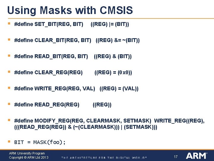
Using Masks with CMSIS § #define SET_BIT(REG, BIT) § #define CLEAR_BIT(REG, BIT) ((REG) &= ~(BIT)) § #define READ_BIT(REG, BIT) ((REG) & (BIT)) § #define CLEAR_REG(REG) ((REG) = (0 x 0)) § #define WRITE_REG(REG, VAL) ((REG) = (VAL)) § #define READ_REG(REG) § #define MODIFY_REG(REG, CLEARMASK, SETMASK) WRITE_REG((REG), (((READ_REG(REG)) & (~(CLEARMASK))) | (SETMASK))) § BIT = MASK(foo); ARM University Program Copyright © ARM Ltd 2013 ((REG) |= (BIT)) ((REG)) 17

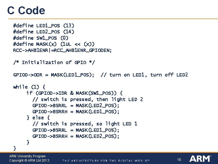
C Code #define LED 1_POS (13) #define LED 2_POS (14) #define SW 1_POS (0) #define MASK(x) (1 UL << (x)) RCC->AHB 1 ENR|=RCC_AHB 1 ENR_GPIODEN; /* Initialization of GPIO */ GPIOD->ODR = MASK(LED 1_POS); while (1) { if (GPIOD->IDR // switch is GPIOD->BSRRL GPIOD->BSRRH } else { // switch is GPIOD->BSRRL GPIOD->BSRRH } } ARM University Program Copyright © ARM Ltd 2013 // turn on LED 1, turn off LED 2 & MASK(SW 1_POS)) { pressed, then light LED 2 = MASK(LED 2_POS); = MASK(LED 1_POS); pressed, so light LED 1 = MASK(LED 1_POS); = MASK(LED 2_POS); 18

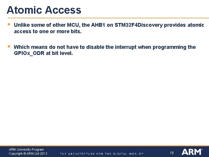
Atomic Access § Unlike some of other MCU, the AHB 1 on STM 32 F 4 Discovery provides atomic access to one or more bits. § Which means do not have to disable the interrupt when programming the GPIOx_ODR at bit level. ARM University Program Copyright © ARM Ltd 2013 19

Inputs and Outputs, Ones and Zeros, Voltages and Currents INTERFACING ARM University Program Copyright © ARM Ltd 2013 20

Inputs: What’s a One? A Zero? § Input signal’s value is determined by voltage § Input threshold voltages depend on supply voltage VDD § Exceeding VDD or GND may damage chip ARM University Program Copyright © ARM Ltd 2013 21

Outputs: What’s a One? A Zero? Nominal output voltages § § § 1: VDD-0. 5 V to VDD 0: 0 to 0. 5 V Note: Output voltage depends on current drawn by load on pin § § Need to consider source-to-drain resistance in the transistor Above values only specified when current < 5 m. A (18 m. A for highdrive pads) and VDD > 2. 7 V Logic 1 out Vout § Logic 0 out Iout ARM University Program Copyright © ARM Ltd 2013 22

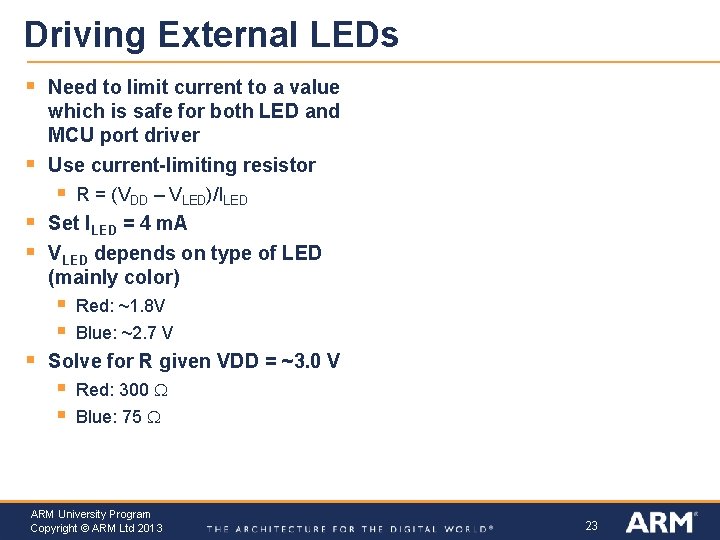
Driving External LEDs § § Need to limit current to a value which is safe for both LED and MCU port driver Use current-limiting resistor § § § Set ILED = 4 m. A VLED depends on type of LED (mainly color) § § § R = (VDD – VLED)/ILED Red: ~1. 8 V Blue: ~2. 7 V Solve for R given VDD = ~3. 0 V § § Red: 300 W Blue: 75 W ARM University Program Copyright © ARM Ltd 2013 23

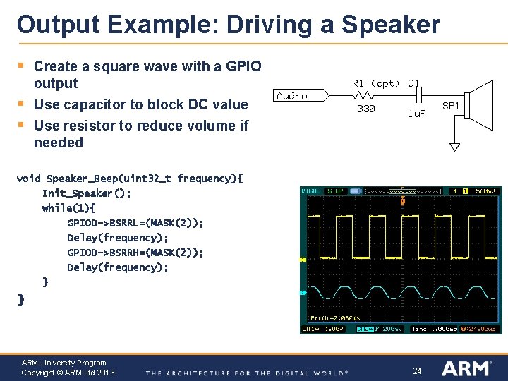
Output Example: Driving a Speaker § Create a square wave with a GPIO output § § Use capacitor to block DC value Use resistor to reduce volume if needed void Speaker_Beep(uint 32_t frequency){ Init_Speaker(); while(1){ GPIOD->BSRRL=(MASK(2)); Delay(frequency); GPIOD->BSRRH=(MASK(2)); Delay(frequency); } } ARM University Program Copyright © ARM Ltd 2013 24