GEN Module GEN Module Overview GEN Module Initialization
- Slides: 34

GEN Module • GEN Module Overview • GEN Module Initialization • General System Control / Status • Watchdog Timer • Cache Control • PLL configuration • Independent Programmable Timers • General Purpose / Special Function Ports • Interrupt Control 1 -1

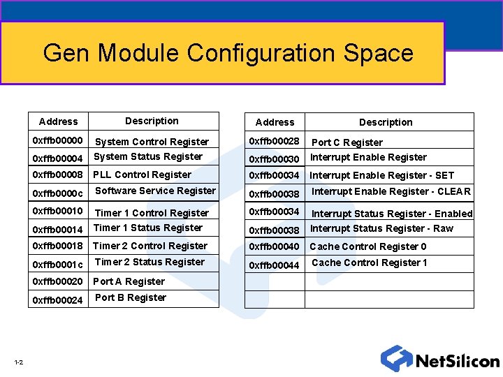
Gen Module Configuration Space 1 -2 Address Description Address 0 xffb 00000 System Control Register 0 xffb 00028 Port C Register 0 xffb 00004 System Status Register 0 xffb 00030 Interrupt Enable Register 0 xffb 00008 PLL Control Register 0 xffb 00034 Interrupt Enable Register - SET 0 xffb 0000 c Software Service Register 0 xffb 00038 Interrupt Enable Register - CLEAR 0 xffb 00010 Timer 1 Control Register 0 xffb 00034 Interrupt Status Register - Enabled 0 xffb 00014 Timer 1 Status Register 0 xffb 00038 Interrupt Status Register - Raw 0 xffb 00018 Timer 2 Control Register 0 xffb 00040 Cache Control Register 0 0 xffb 0001 c Timer 2 Status Register 0 xffb 00044 Cache Control Register 1 0 xffb 00020 Port A Register 0 xffb 00024 Port B Register Description

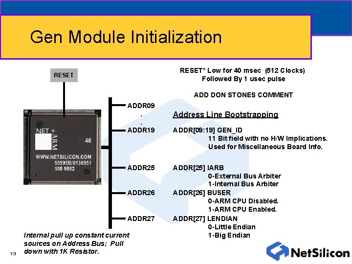
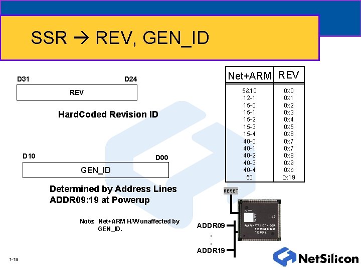
Gen Module Initialization RESET* Low for 40 msec (512 Clocks) Followed By 1 usec pulse RESET ADD DON STONES COMMENT ADDR 09. . ADDR 19 ADDR 25 ADDR 26 ADDR 27 1 -3 Internal pull up constant current sources on Address Bus; Pull down with 1 K Resistor. Address Line Bootstrapping ADDR[09: 19] GEN_ID 11 Bit field with no H/W Implications. Used for Miscellaneous Board Info. ADDR[25] IARB 0 -External Bus Arbiter 1 -Internal Bus Arbiter ADDR[26] BUSER 0 -ARM CPU Disabled. 1 -ARM CPU Enabled. ADDR[27] LENDIAN 0 -Little Endian 1 -Big Endian

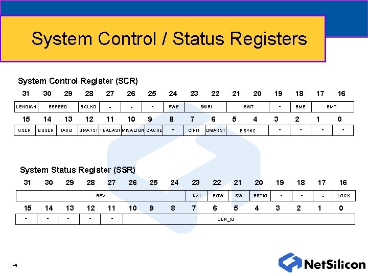
System Control / Status Registers System Control Register (SCR) 31 LENDIAN 15 USER 30 29 BSPEED 14 BUSER 13 IARB 28 27 26 25 24 BCLKD - - - SWE 12 11 10 9 DMATST TEALAST MISALIGN CACHE 8 - 23 22 21 SWRI 7 CINIT 20 SWT 6 5 DMARST 4 BSYNC 19 18 - BME 16 17 BMT 3 - 2 - 1 0 - - System Status Register (SSR) 31 30 29 28 27 26 25 24 REV 15 - 1 -4 14 - 13 - 12 - 11 - 10 9 8 23 22 21 20 19 18 17 16 EXT POW SW RSTIO - - - LOCK 7 6 5 GEN_ID 4 3 2 1 0

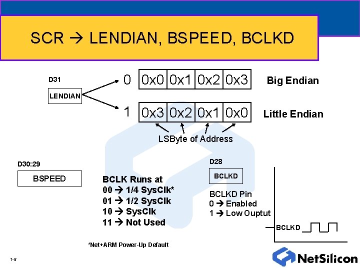
SCR LENDIAN, BSPEED, BCLKD D 31 0 0 x 1 0 x 2 0 x 3 Big Endian 1 0 x 3 0 x 2 0 x 1 0 x 0 Little Endian LENDIAN LSByte of Address D 28 D 30: 29 BSPEED BCLK Runs at 00 1/4 Sys. Clk* 01 1/2 Sys. Clk 10 Sys. Clk 11 Not Used *Net+ARM Power-Up Default 1 -5 BCLKD Pin 0 Enabled 1 Low Ouptut BCLKD

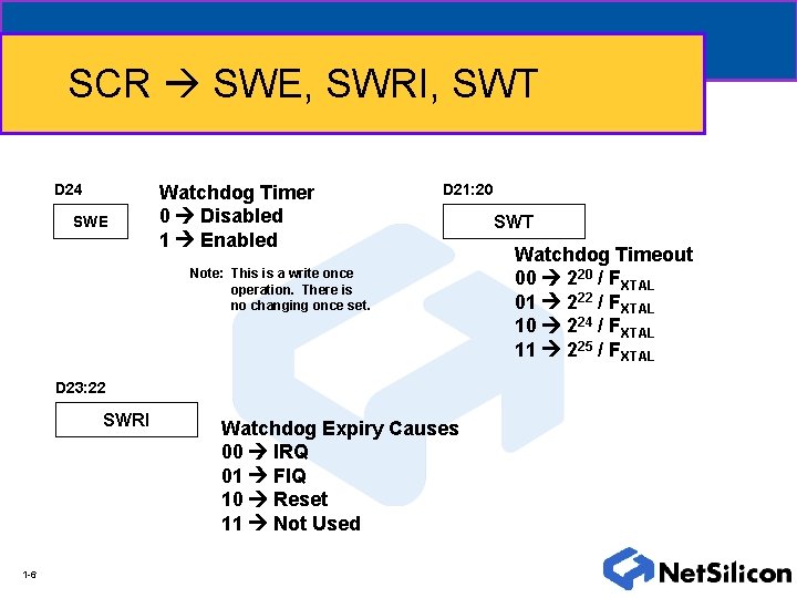
SCR SWE, SWRI, SWT D 24 SWE Watchdog Timer 0 Disabled 1 Enabled D 21: 20 Note: This is a write once operation. There is no changing once set. D 23: 22 SWRI 1 -6 Watchdog Expiry Causes 00 IRQ 01 FIQ 10 Reset 11 Not Used SWT Watchdog Timeout 00 220 / FXTAL 01 222 / FXTAL 10 224 / FXTAL 11 225 / FXTAL

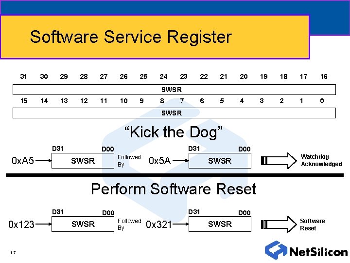
Software Service Register 31 30 29 28 27 26 25 24 23 22 21 20 19 18 17 16 6 5 4 3 2 1 0 SWSR 15 14 13 12 11 10 9 8 7 SWSR “Kick the Dog” D 31 0 x. A 5 D 31 D 00 Followed By SWSR 0 x 5 A D 00 Watchdog Acknowledged SWSR Perform Software Reset D 31 0 x 123 1 -7 D 31 D 00 SWSR Followed By 0 x 321 D 00 SWSR Software Reset

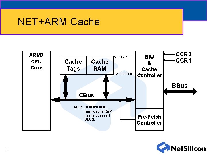
NET+ARM Cache ARM 7 CPU Core 0 x. FFF 0 3 FFF Cache Tags Cache RAM 0 x. FFF 0 0000 BIU & Cache Controller CCR 0 CCR 1 BBus CBus Note: Data fetched from Cache RAM need not assert BBUS. 1 -8 Pre-Fetch Controller

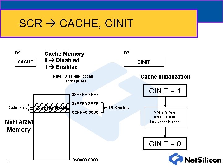
SCR CACHE, CINIT D 9 CACHE Cache Memory 0 Disabled 1 Enabled D 7 CINIT Cache Initialization Note: Disabling cache saves power. CINIT = 1 0 x. FFFF Cache Sets 4 3 2 1 Cache RAM 0 x. FFF 0 3 FFF 0 x. FFF 0 0000 Net+ARM Memory 16 Kbytes Write ‘ 0’ from 0 x. FFF 0 0000 thru 0 x. FFFF 3 FFF CINIT = 0 1 -9 0 x 0000

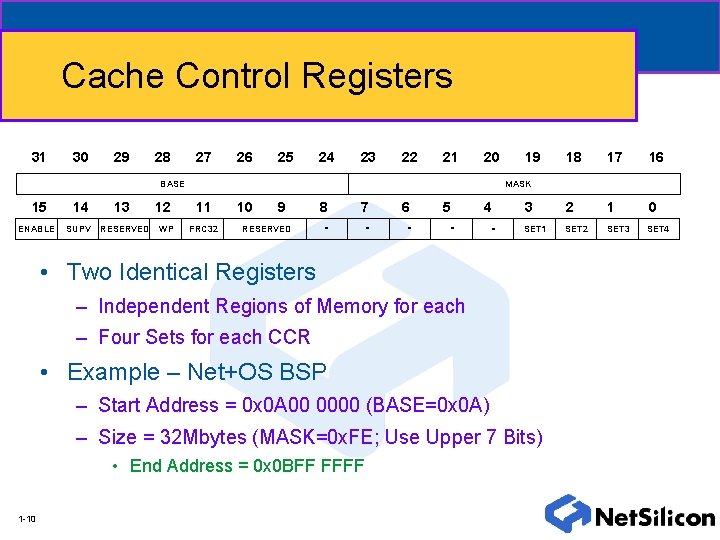
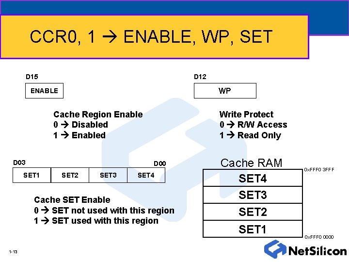
Cache Control Registers 31 30 29 28 27 26 25 24 23 22 21 20 BASE 15 ENABLE 14 SUPV 13 RESERVED 12 WP 19 18 17 16 3 2 1 0 SET 1 SET 2 SET 3 SET 4 MASK 11 FRC 32 10 9 RESERVED 8 - 7 - 6 - 5 - 4 - • Two Identical Registers – Independent Regions of Memory for each – Four Sets for each CCR • Example – Net+OS BSP – Start Address = 0 x 0 A 00 0000 (BASE=0 x 0 A) – Size = 32 Mbytes (MASK=0 x. FE; Use Upper 7 Bits) • End Address = 0 x 0 BFF FFFF 1 -10

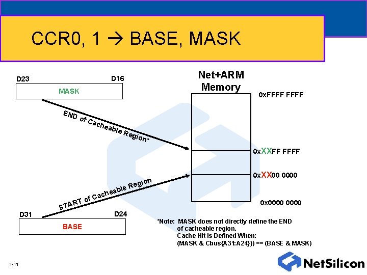
CCR 0, 1 BASE, MASK Net+ARM Memory D 16 D 23 MASK END of C ach eab le 0 x. FFFF Reg ion* 0 x. XXFF FFFF of ART D 31 ST BASE 1 -11 Ca n egio 0 x. XX 00 0000 le R ab che D 24 0 x 0000 *Note: MASK does not directly define the END of cacheable region. Cache Hit is Defined When: (MASK & Cbus{A 31: A 24}}) == (BASE & MASK)

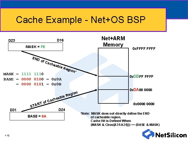
Cache Example - Net+OS BSP Net+ARM Memory D 16 D 23 MASK = FE END of C ach eab le Reg ion* MASK = 1111 1110 BASE = 0000 0100 = 0 x 0 A = 0000 0101 = 0 x 0 B of ART D 31 ST BASE = 0 A 1 -12 Ca 0 x. FFFF 0 x 0 BFF FFFF n egio 0 x 0 A 00 0000 le R ab che D 24 0 x 0000 *Note: MASK does not directly define the END of cacheable region. Cache Hit is Defined When: (MASK & Cbus{A 31: A 24}}) == (BASE & MASK)

CCR 0, 1 ENABLE, WP, SET D 15 D 12 WP ENABLE Write Protect 0 R/W Access 1 Read Only Cache Region Enable 0 Disabled 1 Enabled D 03 D 00 SET 1 SET 2 SET 3 SET 4 Cache SET Enable 0 SET not used with this region 1 SET used with this region 1 -13 Cache RAM SET 4 SET 3 SET 2 SET 1 0 x. FFF 0 3 FFF 0 x. FFF 0 0000

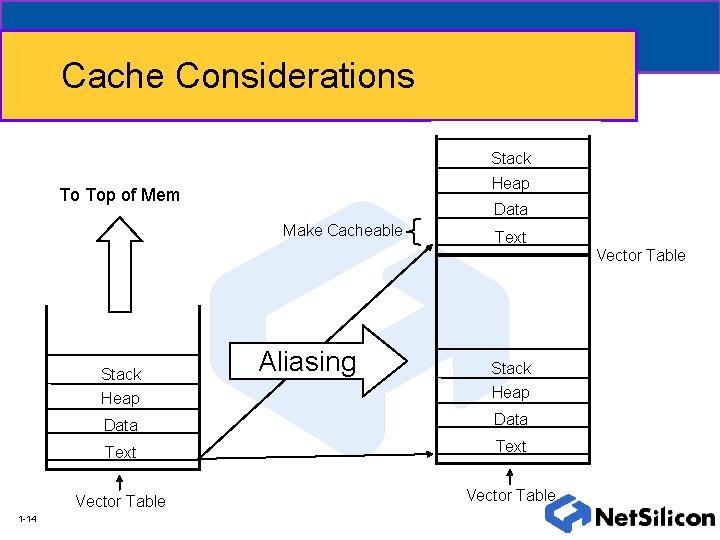
Cache Considerations Stack Heap To Top of Mem Data Make Cacheable Text Vector Table Stack 1 -14 Aliasing Stack Heap Data Text Vector Table

SSR REV, GEN_ID D 31 Net+ARM REV D 24 5&10 12 -1 15 -0 15 -1 15 -2 15 -3 15 -4 40 -0 40 -1 40 -2 40 -3 40 -4 50 REV Hard. Coded Revision ID D 10 D 00 GEN_ID Determined by Address Lines ADDR 09: 19 at Powerup Note: Net+ARM H/W unaffected by GEN_ID. 1 -15 RESET ADDR 09. . ADDR 19 0 x 0 0 x 1 0 x 2 0 x 3 0 x 4 0 x 5 0 x 6 0 x 7 0 x 8 0 x 9 0 xb 0 x 19

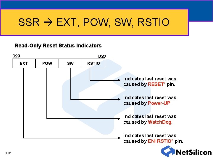
SSR EXT, POW, SW, RSTIO Read-Only Reset Status Indicators D 23 EXT D 20 POW SW RSTIO Indicates last reset was caused by RESET* pin. Indicates last reset was caused by Power-UP. Indicates last reset was caused by Watch. Dog. Indicates last reset was caused by ENI RSTIO* pin. 1 -16

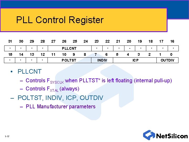
PLL Control Register 31 30 29 28 - - 15 - 14 - 13 - 12 - 27 26 25 24 23 22 21 20 19 18 17 16 - - - - 7 6 PLLCNT 11 10 9 8 POLTST INDIV 5 4 3 ICP 2 1 0 OUTDIV • PLLCNT – Controls FSYSCLK when PLLTST* is left floating (internal pull-up) – Controls FXTAL (always) – POLTST, INDIV, ICP, OUTDIV – PLL Manufacturer parameters 1 -17

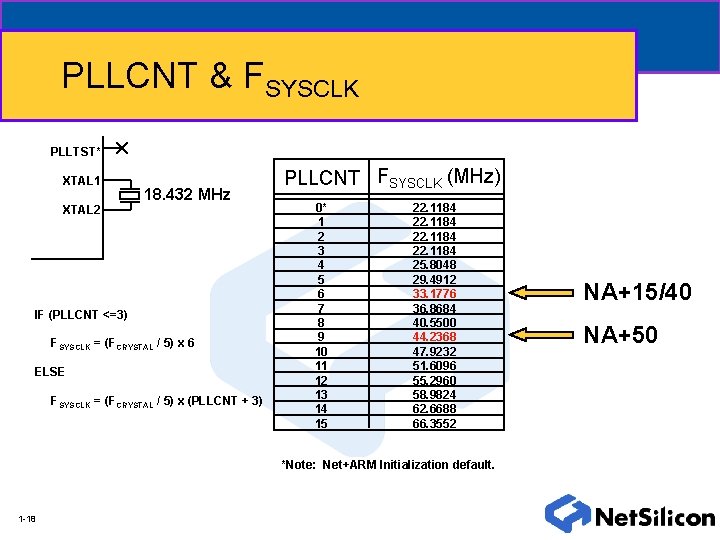
PLLCNT & FSYSCLK PLLTST* XTAL 1 XTAL 2 18. 432 MHz IF (PLLCNT <=3) FSYSCLK = (FCRYSTAL / 5) x 6 ELSE FSYSCLK = (FCRYSTAL / 5) x (PLLCNT + 3) PLLCNT FSYSCLK (MHz) 0* 1 2 3 4 5 6 7 8 9 10 11 12 13 14 15 22. 1184 25. 8048 29. 4912 33. 1776 36. 8684 40. 5500 44. 2368 47. 9232 51. 6096 55. 2960 58. 9824 62. 6688 66. 3552 *Note: Net+ARM Initialization default. 1 -18 NA+15/40 NA+50

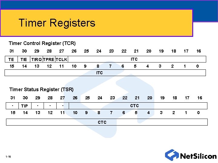
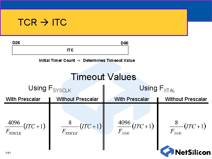
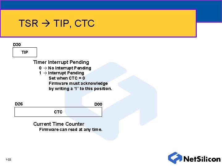
Timer Registers Timer Control Register (TCR) 31 30 TE TIE 15 14 29 28 27 26 25 24 23 22 12 11 20 19 18 17 16 ITC TIRQ TPRE TCLK 13 21 10 9 8 7 6 5 4 3 2 1 0 23 22 21 20 19 18 17 16 4 3 2 1 0 ITC Timer Status Register (TSR) 31 30 29 28 27 - TIP - - - 15 14 13 12 11 26 25 24 CTC 10 9 8 CTC 1 -19 7 6 5

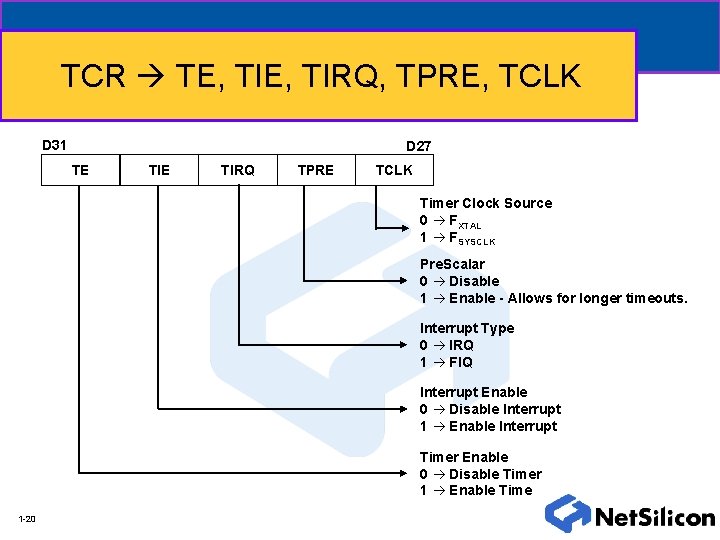
TCR TE, TIRQ, TPRE, TCLK D 31 D 27 TE TIRQ TPRE TCLK Timer Clock Source 0 FXTAL 1 FSYSCLK Pre. Scalar 0 Disable 1 Enable - Allows for longer timeouts. Interrupt Type 0 IRQ 1 FIQ Interrupt Enable 0 Disable Interrupt 1 Enable Interrupt Timer Enable 0 Disable Timer 1 Enable Time 1 -20

TCR ITC D 26 D 00 ITC Initial Timer Count Determines Timeout Values Using FSYSCLK With Prescalar 1 -21 Without Prescalar Using FXTAL With Prescalar Without Prescalar

TSR TIP, CTC D 30 TIP Timer Interrupt Pending 0 No Interrupt Pending 1 Interrupt Pending Set when CTC = 0 Firmware must acknowledge by writing a ‘ 1’ to this position. D 26 D 00 CTC Current Time Counter Firmware can read at any time. 1 -22

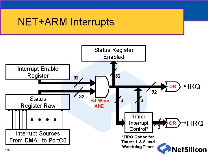
NET+ARM Interrupts Status Register Enabled Interrupt Enable Register Status Register Raw Interrupt Sources From DMA 1 to Port. C 0 1 -23 32 32 32 OR IRQ OR FIRQ 32 Bit-Wise AND 3 3 Timer Interrupt Control* *FIRQ Option for Timers 1 & 2, and Watchdog Timer 3

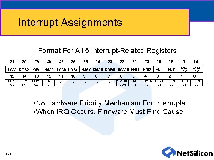
Interrupt Assignments Format For All 5 Interrupt-Related Registers 31 30 29 28 27 26 25 24 23 22 21 DMA 2 DMA 3 DMA 4 DMA 5 DMA 6 DMA 7 DMA 8 DMA 9 DMA 10 ENI 1 15 SER 1 RX 14 13 12 SER 1 TX SER 2 RX SER 2 TX 11 - 10 - 9 - 8 - 7 - 6 5 WATCH TIMER DOG 1 20 19 18 17 16 ENI 2 ENI 3 ENI 4 ENET RX ENET TX 4 3 2 1 0 PORT C 1 PORT C 0 TIMER PORT 2 C 3 PORT C 2 • No Hardware Priority Mechanism For Interrupts • When IRQ Occurs, Firmware Must Find Cause 1 -24

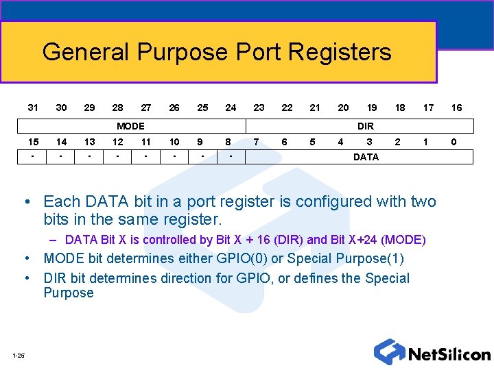
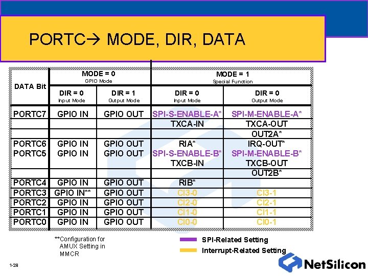
General Purpose Port Registers 31 30 29 28 27 26 25 24 23 22 21 20 MODE 15 - 14 - 13 - 12 - 11 - 19 18 17 16 2 1 0 DIR 10 - 9 - 8 - 7 6 5 4 3 DATA • Each DATA bit in a port register is configured with two bits in the same register. – DATA Bit X is controlled by Bit X + 16 (DIR) and Bit X+24 (MODE) • MODE bit determines either GPIO(0) or Special Purpose(1) • DIR bit determines direction for GPIO, or defines the Special Purpose 1 -25

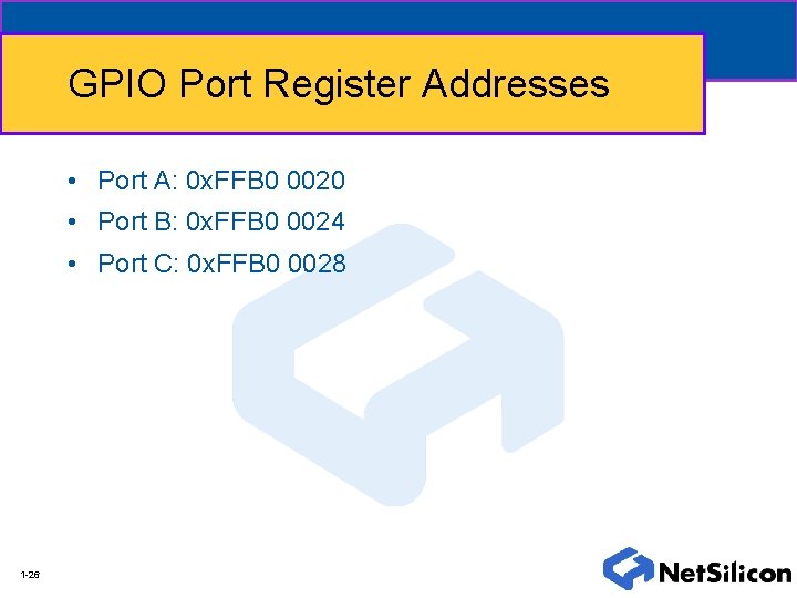
GPIO Port Register Addresses • Port A: 0 x. FFB 0 0020 • Port B: 0 x. FFB 0 0024 • Port C: 0 x. FFB 0 0028 1 -26

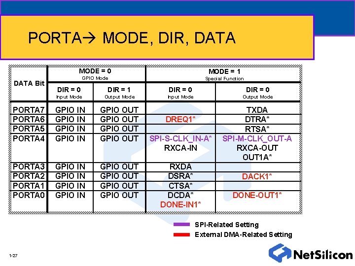
PORTA MODE, DIR, DATA Bit MODE = 0 MODE = 1 GPIO Mode Special Function DIR = 0 DIR = 1 DIR = 0 Input Mode Output Mode PORTA 7 PORTA 6 PORTA 5 PORTA 4 GPIO IN GPIO OUT PORTA 3 PORTA 2 PORTA 1 PORTA 0 GPIO IN GPIO OUT DREQ 1* SPI-S-CLK_IN-A* RXCA-IN RXDA DSRA* CTSA* DCDA* DONE-IN 1* TXDA DTRA* RTSA* SPI-M-CLK_OUT-A RXCA-OUT 1 A* DACK 1* DONE-OUT 1* SPI-Related Setting External DMA-Related Setting 1 -27

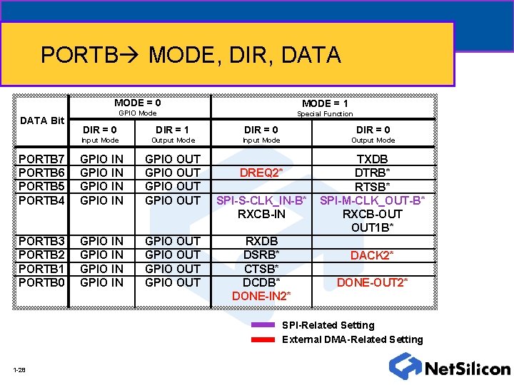
PORTB MODE, DIR, DATA Bit MODE = 0 MODE = 1 GPIO Mode Special Function DIR = 0 DIR = 1 DIR = 0 Input Mode Output Mode PORTB 7 PORTB 6 PORTB 5 PORTB 4 GPIO IN GPIO OUT PORTB 3 PORTB 2 PORTB 1 PORTB 0 GPIO IN GPIO OUT DREQ 2* SPI-S-CLK_IN-B* RXCB-IN RXDB DSRB* CTSB* DCDB* DONE-IN 2* TXDB DTRB* RTSB* SPI-M-CLK_OUT-B* RXCB-OUT 1 B* DACK 2* DONE-OUT 2* SPI-Related Setting External DMA-Related Setting 1 -28

PORTC MODE, DIR, DATA Bit MODE = 0 MODE = 1 GPIO Mode Special Function DIR = 0 DIR = 1 DIR = 0 Input Mode Output Mode PORTC 7 GPIO IN GPIO OUT SPI-S-ENABLE-A* TXCA-IN PORTC 6 PORTC 5 GPIO IN GPIO OUT RIA* SPI-S-ENABLE-B* TXCB-IN SPI-M-ENABLE-A* TXCA-OUT 2 A* IRQ-OUT* SPI-M-ENABLE-B* TXCB-OUT 2 B* GPIO OUT GPIO OUT RIB* CI 3 -0 CI 2 -0 CI 1 -0 CI 0 -0 PORTC 4 GPIO IN PORTC 3 GPIO IN** PORTC 2 GPIO IN PORTC 1 GPIO IN PORTC 0 GPIO IN **Configuration for AMUX Setting in MMCR 1 -29 CI 3 -1 CI 2 -1 CI 1 -1 CI 0 -1 SPI-Related Setting Interrupt-Related Setting

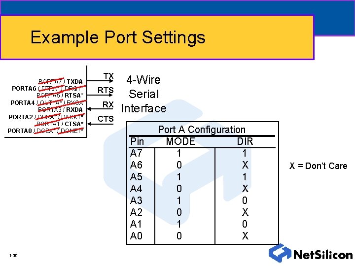
Example Port Settings PORTA 7 / TXDA PORTA 6 / DTRA* / DRQ 1* PORTA 5 / RTSA* PORTA 4 / OUT 1 A* / RXCA PORTA 3 / RXDA PORTA 2 / DSRA* / DACK 1* PORTA 1 / CTSA* PORTA 0 / DCDA* / DONE 1* TX RTS RX CTS 4 -Wire Serial Interface Pin A 7 A 6 A 5 A 4 A 3 A 2 A 1 A 0 1 -30 Port A Configuration MODE DIR 1 1 0 X 1 0 0 X X = Don’t Care

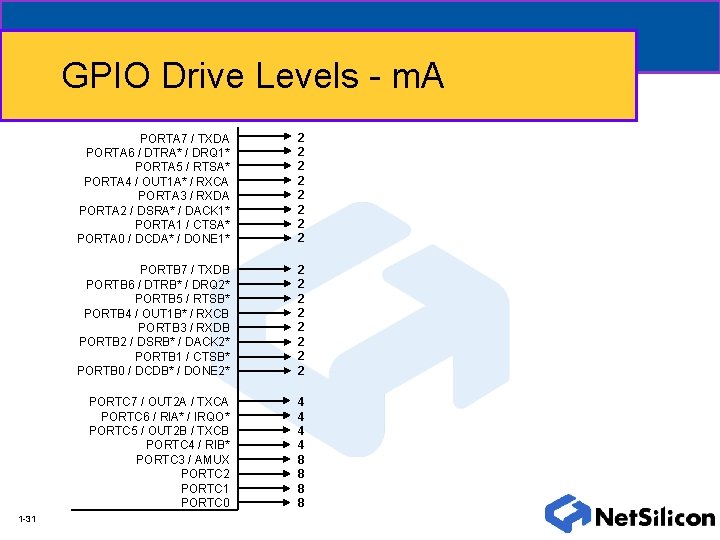
GPIO Drive Levels - m. A 1 -31 PORTA 7 / TXDA PORTA 6 / DTRA* / DRQ 1* PORTA 5 / RTSA* PORTA 4 / OUT 1 A* / RXCA PORTA 3 / RXDA PORTA 2 / DSRA* / DACK 1* PORTA 1 / CTSA* PORTA 0 / DCDA* / DONE 1* 2 2 2 2 PORTB 7 / TXDB PORTB 6 / DTRB* / DRQ 2* PORTB 5 / RTSB* PORTB 4 / OUT 1 B* / RXCB PORTB 3 / RXDB PORTB 2 / DSRB* / DACK 2* PORTB 1 / CTSB* PORTB 0 / DCDB* / DONE 2* 2 2 2 2 PORTC 7 / OUT 2 A / TXCA PORTC 6 / RIA* / IRQO* PORTC 5 / OUT 2 B / TXCB PORTC 4 / RIB* PORTC 3 / AMUX PORTC 2 PORTC 1 PORTC 0 4 4 8 8

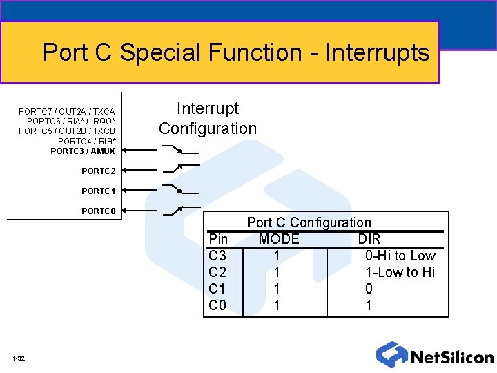
Port C Special Function - Interrupts PORTC 7 / OUT 2 A / TXCA PORTC 6 / RIA* / IRQO* PORTC 5 / OUT 2 B / TXCB PORTC 4 / RIB* PORTC 3 / AMUX Interrupt Configuration PORTC 2 PORTC 1 PORTC 0 Pin C 3 C 2 C 1 C 0 1 -32 Port C Configuration MODE DIR 1 0 -Hi to Low 1 1 -Low to Hi 1 0 1 1

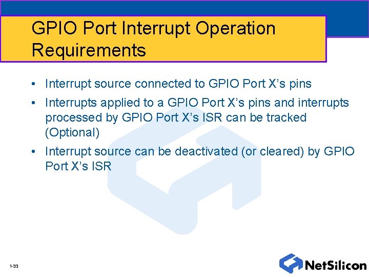
GPIO Port Interrupt Operation Requirements • Interrupt source connected to GPIO Port X’s pins • Interrupts applied to a GPIO Port X’s pins and interrupts processed by GPIO Port X’s ISR can be tracked (Optional) • Interrupt source can be deactivated (or cleared) by GPIO Port X’s ISR 1 -33

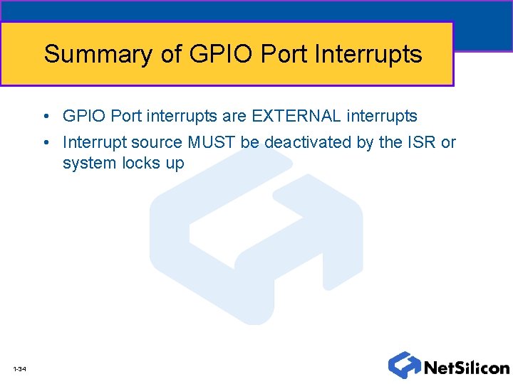
Summary of GPIO Port Interrupts • GPIO Port interrupts are EXTERNAL interrupts • Interrupt source MUST be deactivated by the ISR or system locks up 1 -34