Gate Array Technology IBM 1970 s z Simple
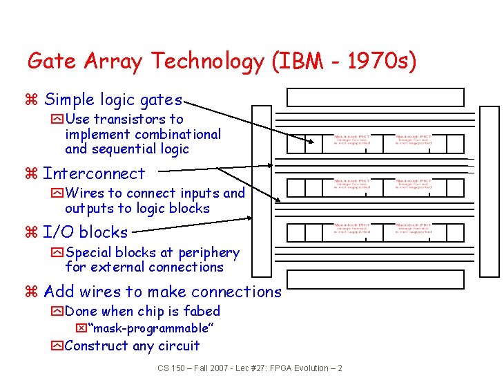
Gate Array Technology (IBM - 1970 s) z Simple logic gates y Use transistors to implement combinational and sequential logic z Interconnect y Wires to connect inputs and outputs to logic blocks z I/O blocks y Special blocks at periphery for external connections z Add wires to make connections y Done when chip is fabed x“mask-programmable” y Construct any circuit CS 150 – Fall 2007 - Lec #27: FPGA Evolution – 2
Programmable Logic z Disadvantages of the Data Book method y Constrained to parts in the Data Book y Parts are necessarily small and standard y Need to stock many different parts z Programmable logic y Use a single chip (or a small number of chips) y Program it for the circuit you want y No reason for the circuit to be small CS 150 – Fall 2007 - Lec #27: FPGA Evolution – 3
Programmable Logic Technologies z Fuse and anti-fuse y Fuse makes or breaks link between two wires y Typical connections are 50 -300 ohm y One-time programmable (testing before programming? ) y Very high density z EPROM and EEPROM y High power consumption y Typical connections are 2 K-4 K ohm y Fairly high density z RAM-based y Memory bit controls a switch that connects/disconnects two wires y Typical connections are. 5 K-1 K ohm y Can be programmed and re-programmed in the circuit y Low density CS 150 – Fall 2007 - Lec #27: FPGA Evolution – 4
Making Large Programmable Logic Circuits z Alternative 1 : “CPLD” y Put a lot of PLDS on a chip y Add wires between them whose connections can be programmed y Use fuse/EEPROM technology z Alternative 2: “FPGA” y Emulate gate array technology y Hence Field Programmable Gate Array y You need: x. A way to implement logic gates x. A way to connect them together CS 150 – Fall 2007 - Lec #27: FPGA Evolution – 10
Field-Programmable Gate Arrays z PALs, PLAs = 10 s – 100 s Gate Equivalents z Field Programmable Gate Arrays = FPGAs y Altera MAX Family y Actel Programmable Gate Array y Xilinx Logical Cell Array z 1000 s - 100000(s) of Gate Equivalents! CS 150 – Fall 2007 - Lec #27: FPGA Evolution – 11

Field-Programmable Gate Arrays z Logic blocks y To implement combinational and sequential logic z Interconnect y Wires to connect inputs and outputs to logic blocks z I/O blocks y Special logic blocks at periphery of device for external connections z Key questions: y How to make logic blocks programmable? y How to connect the wires? y After the chip has been fab’d CS 150 – Fall 2007 - Lec #27: FPGA Evolution – 12
Tradeoffs in FPGAs z Logic block - how are functions implemented: fixed functions (manipulate inputs) or programmable? y Support complex functions, need fewer blocks, but they are bigger so less of them on chip y Support simple functions, need more blocks, but they are smaller so more of them on chip z Interconnect y How are logic blocks arranged? y How many wires will be needed between them? y Are wires evenly distributed across chip? y Programmability slows wires down – are some wires specialized to long distances? y How many inputs/outputs must be routed to/from each logic block? y What utilization are we willing to accept? 50%? 20%? 90%? CS 150 – Fall 2007 - Lec #27: FPGA Evolution – 13
Altera EPLD (Erasable Programmable Logic Devices) z Historical Perspective y PALs: same technology as programmed once bipolar PROM y EPLDs: CMOS erasable programmable ROM (EPROM) erased by UV light z Altera building block = MACROCELL 8 Product Term AND-OR Array + Programmable MUX's I/O Pin Seq. Logic Block Programmable polarity Programmable feedback CS 150 – Fall 2007 - Lec #27: FPGA Evolution – 14
Altera EPLD: Synchronous vs. Asynchronous Mode Altera EPLDs contain 10 s-100 s of independently programmed macrocells Personalized by EPROM bits: Flipflop controlled by global clock signal local signal computes output enable Flipflop controlled by locally generated clock signal + Seq Logic: could be D, T positive or negative edge triggered + product term to implement clear function CS 150 – Fall 2007 - Lec #27: FPGA Evolution – 15
Altera Multiple Array Matrix (MAX) AND-OR structures are relatively limited Cannot share signals/product terms among macrocells Logic Array Blocks Global Routing: Programmable Interconnect Array (similar to macrocells) EPM 5128: 8 Fixed Inputs 52 I/O Pins 8 LABs 16 Macrocells/LAB 32 Expanders/LAB CS 150 – Fall 2007 - Lec #27: FPGA Evolution – 16
LAB Architecture I/O Pad Macrocell ARRAY I N P U T S I/O Block I/O Pad P I A Expander Product Term ARRAY Expander Terms shared among all macrocells within the LAB • Efficient way to use AND plane resources CS 150 – Fall 2007 - Lec #27: FPGA Evolution – 17
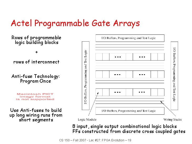
Actel Programmable Gate Arrays Rows of programmable logic building blocks + rows of interconnect Anti-fuse Technology: Program Once Use Anti-fuses to build up long wiring runs from short segments 8 input, single output combinational logic blocks FFs constructed from discrete cross coupled gates CS 150 – Fall 2007 - Lec #27: FPGA Evolution – 19
Actel Logic Module Basic Module is a Modified 4: 1 Multiplexer Example: Implementation of S-R Latch CS 150 – Fall 2007 - Lec #27: FPGA Evolution – 20
Actel Interconnection Fabric CS 150 – Fall 2007 - Lec #27: FPGA Evolution – 21
Actel Routing Example Jogs cross an anti-fuse minimize the # of jogs for speed critical circuits 2 - 3 hops for most interconnections CS 150 – Fall 2007 - Lec #27: FPGA Evolution – 22
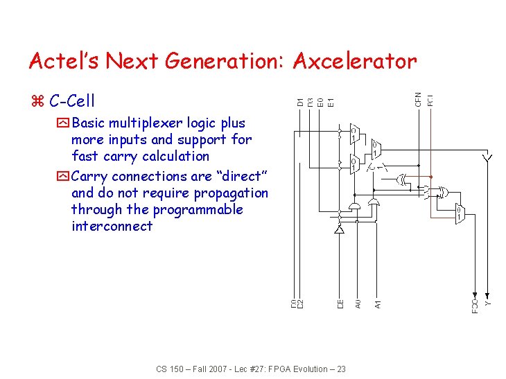
Actel’s Next Generation: Axcelerator z C-Cell y Basic multiplexer logic plus more inputs and support for fast carry calculation y Carry connections are “direct” and do not require propagation through the programmable interconnect CS 150 – Fall 2007 - Lec #27: FPGA Evolution – 23
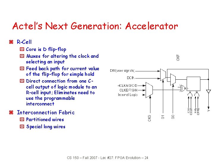
Actel’s Next Generation: Accelerator z R-Cell y Core is D flip-flop y Muxes for altering the clock and selecting an input y Feed back path for current value of the flip-flop for simple hold y Direct connection from one Ccell output of logic module to an R-cell input; Eliminates need to use the programmable interconnect z Interconnection Fabric y Partitioned wires y Special long wires CS 150 – Fall 2007 - Lec #27: FPGA Evolution – 24
Xilinx Programmable Gate Arrays z CLB - Configurable Logic Block y 5 -input, 1 output function y or 2 4 -input, 1 output functions y optional register on outputs z Built-in fast carry logic z Can be used as memory z Three types of routing y direct y general-purpose y long lines of various lengths z RAM-programmable y can be reconfigured CS 150 – Fall 2007 - Lec #27: FPGA Evolution – 25
Programmable Interconnect I/O Blocks (IOBs) Configurable Logic Blocks (CLBs) CS 150 – Fall 2007 - Lec #27: FPGA Evolution – 26
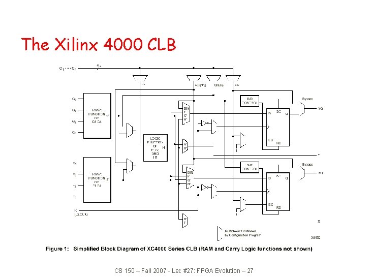
The Xilinx 4000 CLB CS 150 – Fall 2007 - Lec #27: FPGA Evolution – 27
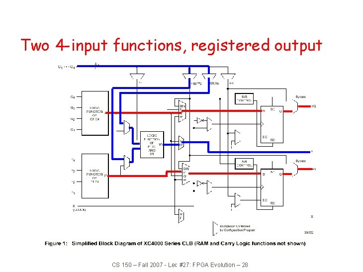
Two 4 -input functions, registered output CS 150 – Fall 2007 - Lec #27: FPGA Evolution – 28
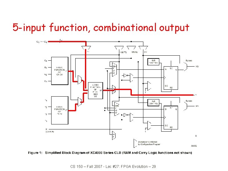
5 -input function, combinational output CS 150 – Fall 2007 - Lec #27: FPGA Evolution – 29
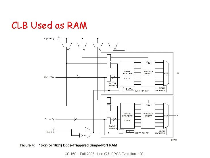
CLB Used as RAM CS 150 – Fall 2007 - Lec #27: FPGA Evolution – 30
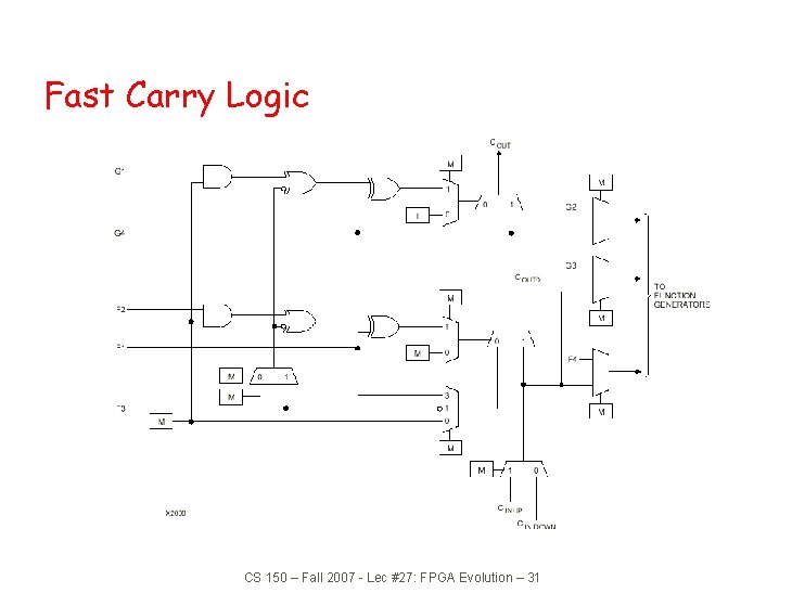
Fast Carry Logic CS 150 – Fall 2007 - Lec #27: FPGA Evolution – 31
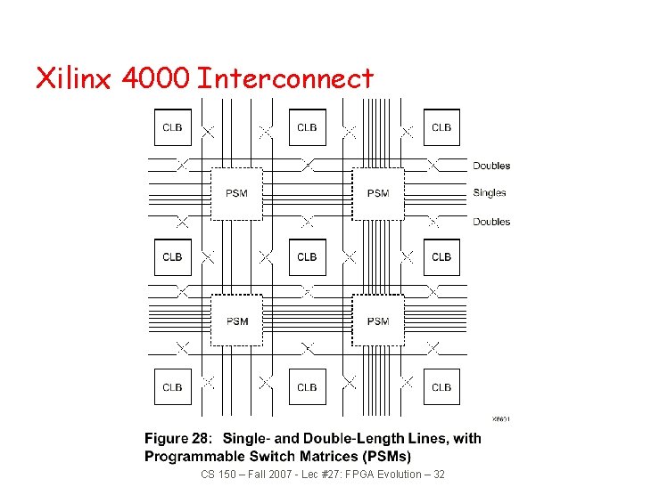
Xilinx 4000 Interconnect CS 150 – Fall 2007 - Lec #27: FPGA Evolution – 32
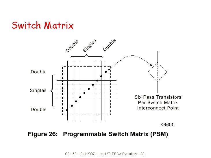
Switch Matrix CS 150 – Fall 2007 - Lec #27: FPGA Evolution – 33
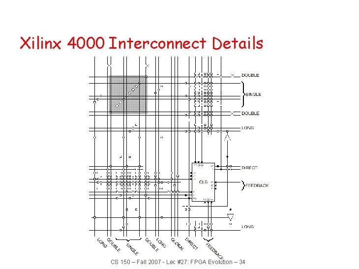
Xilinx 4000 Interconnect Details CS 150 – Fall 2007 - Lec #27: FPGA Evolution – 34
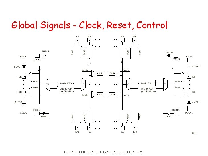
Global Signals - Clock, Reset, Control CS 150 – Fall 2007 - Lec #27: FPGA Evolution – 35
Xilinx Vertex-II Family z 88 -1000+ pins z 64 -10000+ CLBs y Combinational and sequential logic using lookup tables and flip-flops y Random-access memory y Shift registers for use as buffer storage z Multipliers regularly placed throughout the CLB array to accelerate digital signal processing applications z E. g. , the XC 2 V 8000: 11, 648 CLBs, 1108 IOBs, 90, 000+ FFs, 3 Mbits RAM (168 x 18 Kbit blocks), 168 multipliers y Equivalent to eight million two-input gates! CS 150 – Fall 2007 - Lec #27: FPGA Evolution – 40
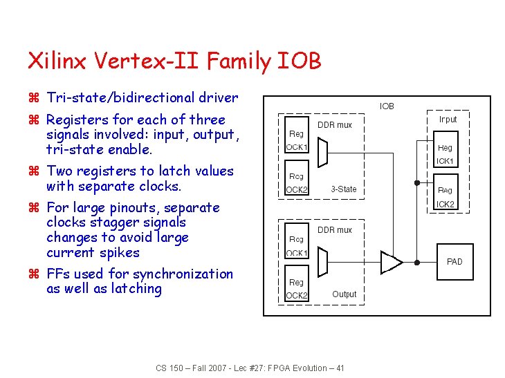
Xilinx Vertex-II Family IOB z Tri-state/bidirectional driver z Registers for each of three signals involved: input, output, tri-state enable. z Two registers to latch values with separate clocks. z For large pinouts, separate clocks stagger signals changes to avoid large current spikes z FFs used for synchronization as well as latching CS 150 – Fall 2007 - Lec #27: FPGA Evolution – 41
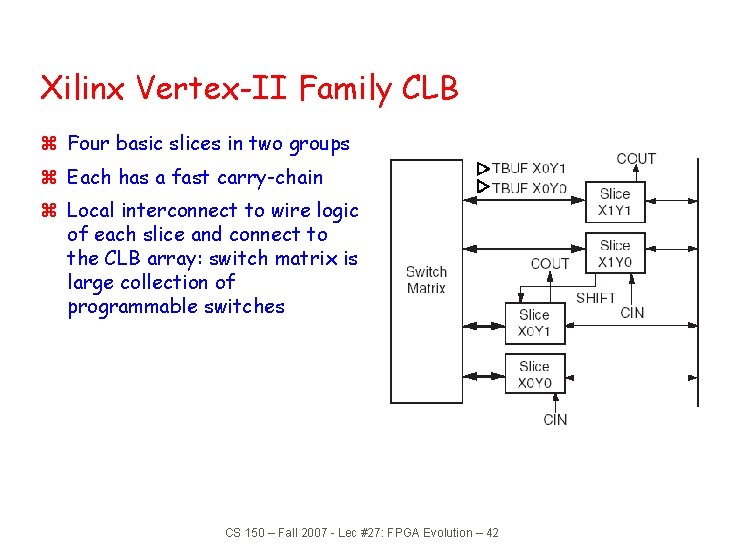
Xilinx Vertex-II Family CLB z Four basic slices in two groups z Each has a fast carry-chain z Local interconnect to wire logic of each slice and connect to the CLB array: switch matrix is large collection of programmable switches CS 150 – Fall 2007 - Lec #27: FPGA Evolution – 42
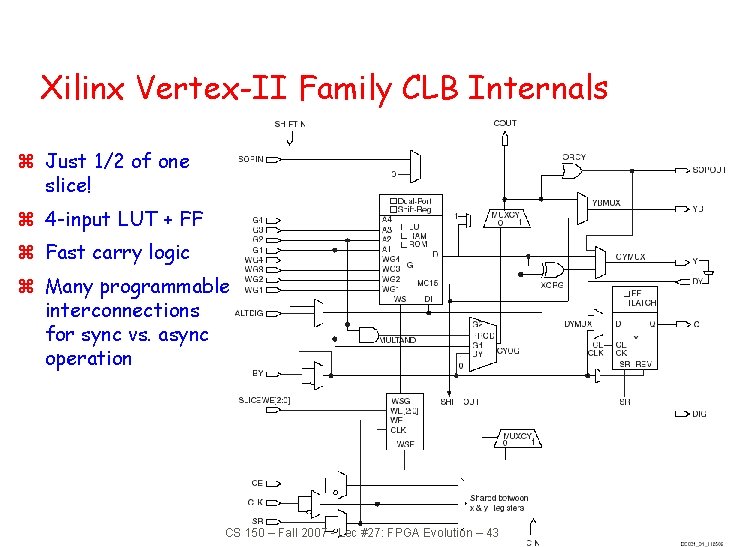
Xilinx Vertex-II Family CLB Internals z Just 1/2 of one slice! z 4 -input LUT + FF z Fast carry logic z Many programmable interconnections for sync vs. async operation CS 150 – Fall 2007 - Lec #27: FPGA Evolution – 43
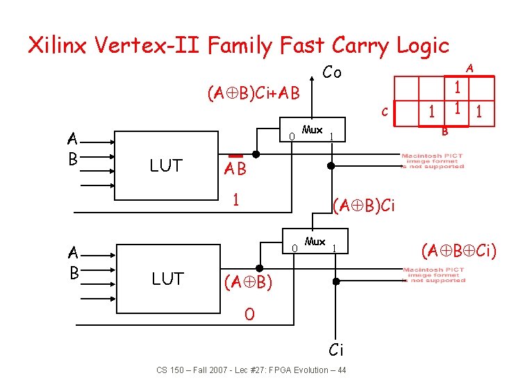
Xilinx Vertex-II Family Fast Carry Logic (AÅB)Ci+AB Co A C A B 0 LUT Mux B (AÅB)Ci 0 LUT 1 AB 1 A B 1 1 Mux 1 (AÅB) 0 Ci CS 150 – Fall 2007 - Lec #27: FPGA Evolution – 44 (AÅBÅCi)
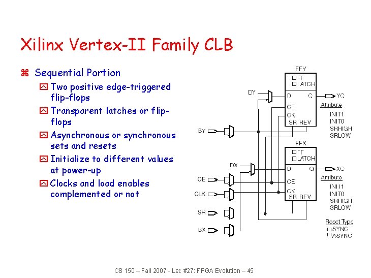
Xilinx Vertex-II Family CLB z Sequential Portion y Two positive edge-triggered flip-flops y Transparent latches or flipflops y Asynchronous or synchronous sets and resets y Initialize to different values at power-up y Clocks and load enables complemented or not CS 150 – Fall 2007 - Lec #27: FPGA Evolution – 45
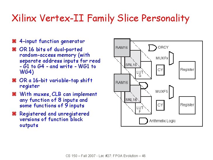
Xilinx Vertex-II Family Slice Personality z 4 -input function generator z OR 16 bits of dual-ported random-access memory (with separate address inputs for read - G 1 to G 4 - and write - WG 1 to WG 4) z OR a 16 -bit variable-tap shift register z With muxes, CLB can implement any function of 8 inputs and some functions of 9 inputs z Registered and unregistered versions of function block outputs CS 150 – Fall 2007 - Lec #27: FPGA Evolution – 46
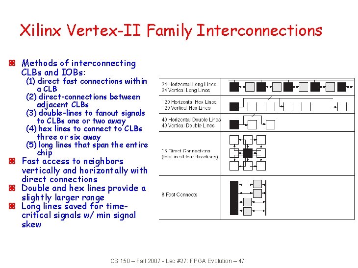
Xilinx Vertex-II Family Interconnections z Methods of interconnecting CLBs and IOBs: (1) direct fast connections within a CLB (2) direct-connections between adjacent CLBs (3) double-lines to fanout signals to CLBs one or two away (4) hex lines to connect to CLBs three or six away (5) long lines that span the entire chip z Fast access to neighbors vertically and horizontally with direct connections z Double and hex lines provide a slightly larger range z Long lines saved for timecritical signals w/ min signal skew CS 150 – Fall 2007 - Lec #27: FPGA Evolution – 47
Programmable Logic Summary z Discrete Gates z Packaged Logic z PLAs z Ever more general architectures of programmable combinational + sequential logic and interconnect y Altera y Actel y Xilinx— 4000 series to Vertex x CLBs implementing logic function generators, RAMs, Shift registers, fast carry logic x Local, inter-CLB, and long line interconnections CS 150 – Fall 2007 - Lec #27: FPGA Evolution – 48
- Slides: 37