Gaseous Detector RD at USTC Gaseous Detector Group
- Slides: 6

Gaseous Detector R&D at USTC Gaseous Detector Group State Key Laboratory of Particle Detection and Electronics University of Science and Technology of China 26 -02 -2018 1

State Key Laboratory of Particle Detection and Electronics Research directions: Human resources: Ø Faculty: 144 Ø Advanced particle detection technology Ø Postdoctor: 32 l Gaseous detectors Ø Student: 324 l Semiconductor detectors l Scintillation detectors Ø Front end electronics l ASIC design and applications Research projects in 2017: 108 l Radiation hardness electronics Funds in 2017: 9. 49 M l High speed waveform sampling l High precision FPGA TDC Ø Large capacity data acquisition and processing system € 2

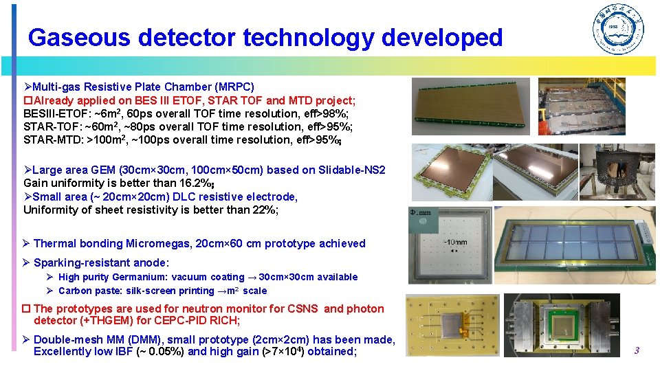
Gaseous detector technology developed ØMulti-gas Resistive Plate Chamber (MRPC) p. Already applied on BES III ETOF, STAR TOF and MTD project; BESIII-ETOF: ~6 m 2, 60 ps overall TOF time resolution, eff>98%; STAR-TOF: ~60 m 2, ~80 ps overall TOF time resolution, eff>95%; STAR-MTD: >100 m 2, ~100 ps overall time resolution, eff>95%; ØLarge area GEM (30 cm× 30 cm, 100 cm× 50 cm) based on Slidable-NS 2 Gain uniformity is better than 16. 2%; ØSmall area (~ 20 cm× 20 cm) DLC resistive electrode, Uniformity of sheet resistivity is better than 22%; Ø Thermal bonding Micromegas, 20 cm× 60 cm prototype achieved Ø Sparking-resistant anode: Ø High purity Germanium: vacuum coating → 30 cm× 30 cm available Ø Carbon paste: silk-screen printing →m 2 scale p The prototypes are used for neutron monitor for CSNS and photon detector (+THGEM) for CEPC-PID RICH; Ø Double-mesh MM (DMM), small prototype (2 cm× 2 cm) has been made, Excellently low IBF (~ 0. 05%) and high gain (>7× 10⁴) obtained; 3

R&D and Projects ongoing MRPC and RPC production ØThin floating glass MRPC → CBM TOF project (Total area ~65 m 2; Time resolution <80 ps; rate ~1 k. Hz/cm 2); ØThin gap RPC → ATLAS phase II upgrade (rate >1 k. Hz/cm 2 ,Time resolution <1 ns; position resolution <1 mm); Large area Micromegas fabrication ØDeveloping the m 2 scale rolling machine → to make m 2 scale Micromegas based on thermal bonding technique; ØLarge area DMM → Photon detection application: RICH → Low IBF application: Picosecond Micromegas, CEPC-TPC, ILC-TPC; New materials ØLarge area resistive electrode based on DLC → New robust resistive electrode for lots of gaseous detectors: Resistive-GEM, Micromgas, μRWELL, …; ØCollaborating with photocathode experts who used to work for low-level light night vision device → Develop new photocathode to replace the fragile Cs. I : High quantum efficiency, robust enough; Human resources of the gaseous detector team: 7 Faculties: Y. Zhou, J. Liu, Z. Zhang, M. Shao, C. Li, Y. Sun, Z. Zhao 12 Students 4

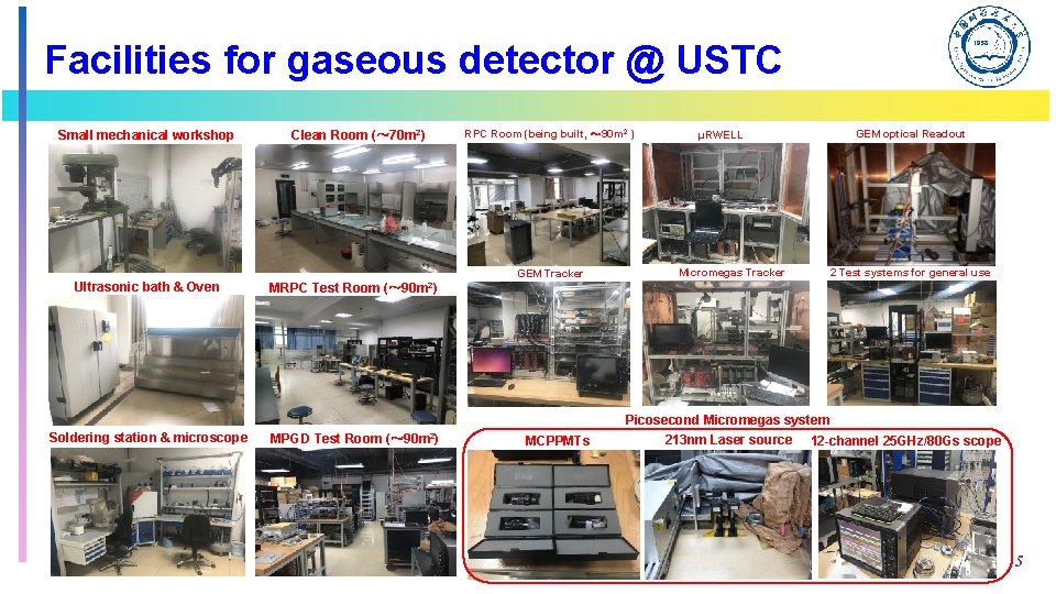
Facilities for gaseous detector @ USTC Small mechanical workshop Ultrasonic bath & Oven Soldering station & microscope Clean Room (~ 70 m 2) RPC Room (being built, ~ 90 m 2 ) GEM Tracker MRPC Test Room (~ 90 m 2) MPGD Test Room (~ 90 m 2) MCPPMTs μRWELL Micromegas Tracker GEM optical Readout 2 Test systems for general use Picosecond Micromegas system 213 nm Laser source 12 -channel 25 GHz/80 Gs scope 5

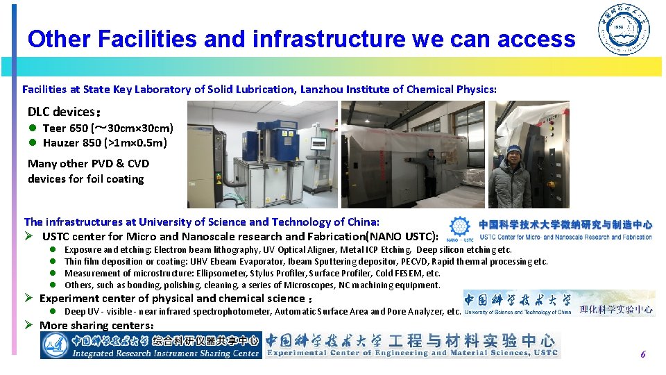
Other Facilities and infrastructure we can access Facilities at State Key Laboratory of Solid Lubrication, Lanzhou Institute of Chemical Physics: DLC devices: l Teer 650 (~ 30 cm× 30 cm) l Hauzer 850 (>1 m× 0. 5 m) Many other PVD & CVD devices for foil coating The infrastructures at University of Science and Technology of China: Ø USTC center for Micro and Nanoscale research and Fabrication(NANO USTC): l l Exposure and etching: Electron beam lithography, UV Optical Aligner, Metal ICP Etching, Deep silicon etching etc. Thin film deposition or coating: UHV Ebeam Evaporator, Ibeam Sputtering depositor, PECVD, Rapid thermal processing etc. Measurement of microstructure: Ellipsometer, Stylus Profiler, Surface Profiler, Cold FESEM, etc. Others, such as bonding, polishing, cleaning, a series of Microscopes, NC machining equipment. Ø Experiment center of physical and chemical science : l Deep UV - visible - near infrared spectrophotometer, Automatic Surface Area and Pore Analyzer, etc. Ø More sharing centers: 6