Ga N based blue LED Joonas Leppnen Emma

Ga. N based blue LED Joonas Leppänen Emma Kiljo Jussi Taskinen Niklas Heikkilä Alexander Permogorov 13. 5. 2016 Photonics School of Electrical Engineering 13. 5. 2016 Group 3 LED

Content 1. 2. 3. 4. 5. 6. Introduction Theoretical Background Manufacturing Applications Future Prospects Conclusions Photonics Group 3: LED 21. 4. 2016

Introduction • First LEDs from late 50’s to early 60’s – Expensive at first, nowadays quite cheap • Green and red LEDs easier to create than blue ones – Higher energy (gap) needed • By combining red, green and blue LEDs, it is possible to create white light – Nobel prize for blue LED in 2014 • Phosphorus coating of blue-LED also provides white light • By replacing incandecent lighting with LEDs, energy can be saved Photonics Group 3: LED 13. 5. 2016

Theoretical Background • The operation princible of LED is based on semiconductor pnjunction • Heterojunction structure is a typical structure used in LEDs – Confinement of the charge carriers in active layer – Reduction of reabsorption • Manipulation of bandgaps by alloying compound semiconductors Photonics Group 3: LED 13. 5. 2016

Theoretical Background • The most important materials for blue LEDs are currently Ga. N based compound semiconductors • Zinc compounds and silicon carbide may also be utilized but they are indirect bandgap semiconductors • Ga. N is direct band gap semiconductor, which provides better efficiency. • Ga. N and most substrates have a large lattice mismatch, sapphire is often used as substrate • P-type Ga. N can be produced by doping with Mg or Zn, and n-type by doping with silicon Photonics Group 3: LED 13. 5. 2016
 • Poor quality (TDD =")
Manufacturing On foreign substrate MOVPE (Metal-Organic Vapour Phase Epitaxy) • Poor quality (TDD = 106 - 109 cm-2) MBE (Molecular Beam Epitaxy) • Better quality MBE MOVPE (TDD = 105 - 106 cm-2) Pros Control of doping Good crystalline quality Slower growth Expensive Composition at the monolayer level Control of doping Faster growth ~ 2µm/h Easier maintenance Widely used in industry Ultra high vacuum required Poisonous precursor gases C and H from precursors are incorporated into layers Photonics Group 3: LED 13. 5. 2016

Manufacturing Bulk Growth • MOVPE and MBE are not cost effective since they are slow when compared to Czochralski for Si • Quality is not that good due to lattice mismatch and other things related to the growth on top of foreign material – Low luminous flux • Bulk growth of Ga. N may overcome these issues using Ga. N seeds which may be grown on foreign substrates • Possibility of higher growth rates for cost effective growth Photonics Group 3: LED 13. 5. 2016
 Process • High quality • Extremely")
Manufacturing Bulk Growth HVPE (Hydride Vapour Phase Epitaxy) Process • High quality • Extremely high growth rate (300 µm/h) • Can be used to grow Ga. N seeds on sapphire or • silicon, which can be removed by a lift-off technique after the growth • Seeded growth is possible but requires high quality seed • (TDD = 104 - 106 cm-2) • FEOL (Front-End of line) process – 1000 ◦C Based on a reaction between Ga. Cl and NH 3 to form Ga. N crystals Ga. Cl is provided via reaction between solid Ga and HCl – the quality is seed quality dependent • HVPE-Ga. N can itself be used as a seed • Wafer bow/bending causes difficulties for larger wafers • Widely used for bulk Ga. N growth at the moment Photonics Group 3: LED 13. 5. 2016
")
Manufacturing Bulk Growth Ammonothermal growth • Higher quality (TDD = 103 - 104 cm-2) • Difficult to handle safely! • Growth rate only 20 µm/h • No bending or cracking issues Process • BEOL (Back-End of line) process – 400 - 500 ◦C – 3500 atm pressure • Grown from polycrystalline Ga. N grains in a supercritical ammonia solution • Can be grown on HVPE seeds but the quality depends on the seed quality Photonics Group 3: LED 13. 5. 2016
 Flux • Extremely high quality (TDD = 102 -")
Manufacturing Bulk Growth Sodium (Na) Flux • Extremely high quality (TDD = 102 - 103 cm-2) • High growth rate of 100 µm/h • No cracking • Still on its early stages! Process • FEOL process – 800 ◦C • Grown in Ga-Na melt on top of seed – MOCVD-Ga. N or HVPE-Ga. N on sapphire, which can be removed afterwards • Necking technique decreases the TDD even if the seed is poor quality! – Reason behind this are unknown Photonics Group 3: LED 13. 5. 2016

Why LED chosen • Incandescent: 17 lm/W • Fluorescent: 90 lm/W • LED: up to 425 lm/W Photonics Group 3: LED 13. 5. 2016

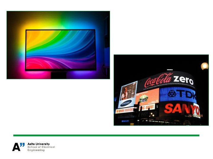
LED in illumination

Blue LED to white light: phosphors • Ce 3+: YAG • Excited by LED radiation • Blue + Yellow = White • Highest efficiency – 425 lm/W • Reasonable Color Rendering Index (CRI)

Blue LED to white light: color mixing • Efficiency lower than for phosphors – 300 lm/W • Highest CRI • Possibility of color changing

Future Prospects Driving Forces of the blue-LED technology • US DOE plan that 70 % of public lights will be replaced by LED’s til 2030 • Pressure to lower price and increasing efficiency and lumens. Photonics Group 3: LED 13. 5. 2016

Conclusions • First LEDs in the 60’s • Blue LEDs enabled white light • Current manufacturing methods can be used – A need for better quality and more cost-effective wafers – Bulk growth may be the answer • HVPE+MOVPE-seed is currently used but the TDD must be decreased • Na-flux seems most promising in the future but size must be increased • Superior lumen per watt production – Major possibilities for energy saving Photonics Group 3: LED 21. 4. 2016

Thanks! Photonics Group 3: LED 21. 4. 2016
- Slides: 18