FUTURE IC TEST CHALLENGES QUALITY COST AND TIME







- Slides: 43

FUTURE IC TEST CHALLENGES QUALITY, COST AND TIME TO MARKET Korea test conference workshop 2014 Jin-Soo Ko Teradyne Inc. Jin-soo. ko@Teradyne. com Korea test workshop Oct. 15 2014 Jin-Soo Ko

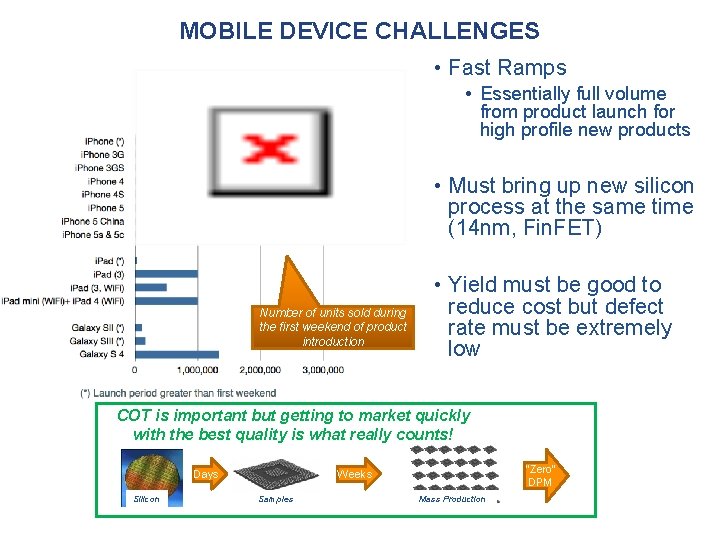
MOBILE DEVICE CHALLENGES • Fast Ramps • Essentially full volume from product launch for high profile new products • Must bring up new silicon process at the same time (14 nm, Fin. FET) Number of units sold during the first weekend of product introduction • Yield must be good to reduce cost but defect rate must be extremely low COT is important but getting to market quickly with the best quality is what really counts! Days Silicon “Zero” DPM Weeks Samples Mass Production

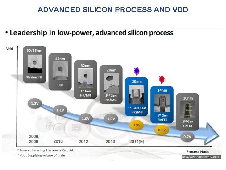
ADVANCED SILICON PROCESS AND VDD

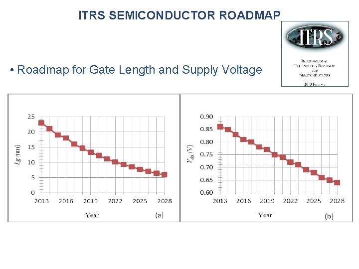
ITRS SEMICONDUCTOR ROADMAP • Roadmap for Gate Length and Supply Voltage

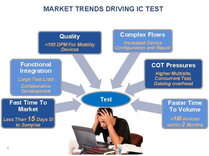
MARKET TRENDS DRIVING IC TEST Quality Complex Flows <100 DPM For Mobility Devices Increased Device Configuration and Repair Functional Integration COT Pressures Higher Multisite, Concurrent Test, Datalog overhead Large Test Lists Collaborative Development Fast Time To Market Less Than 15 Days Si to Samples 5 Test Faster Time To Volume >1 M devices within 2 Months

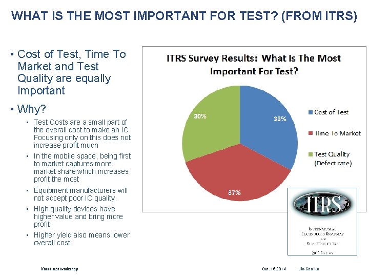
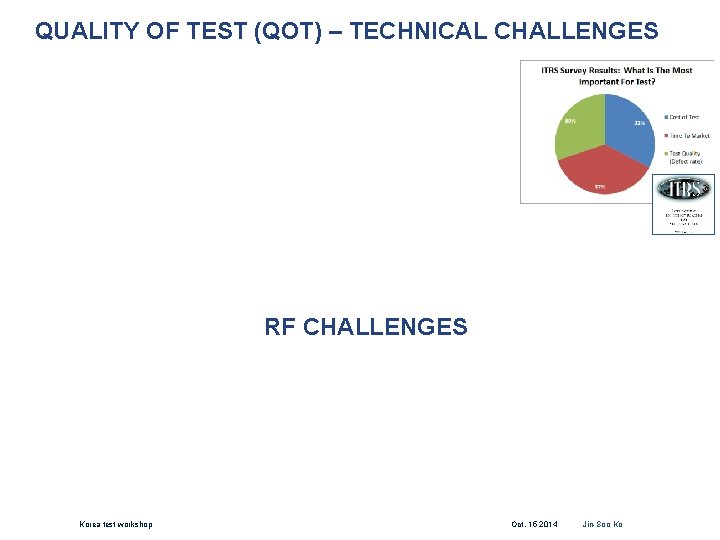
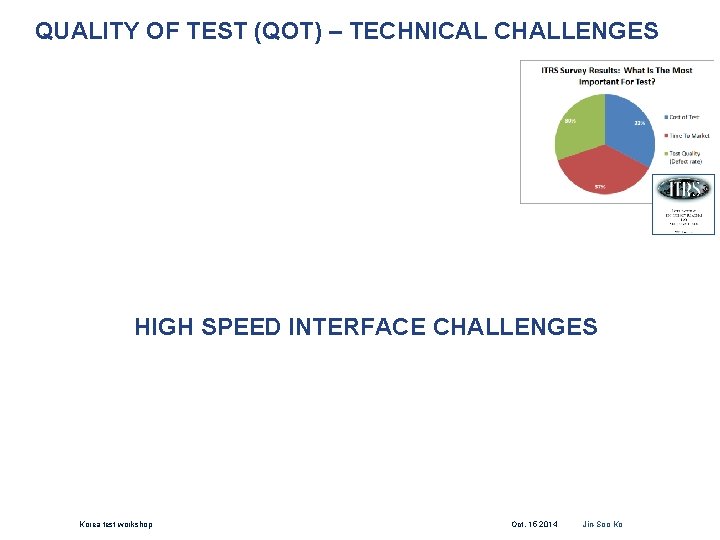
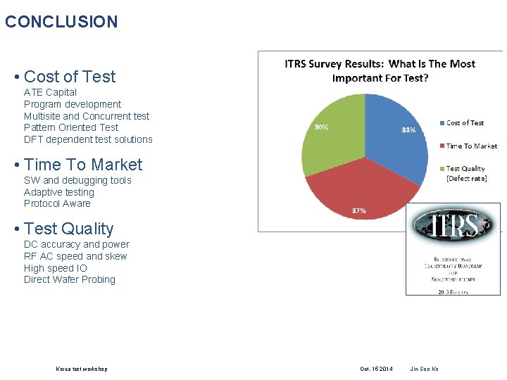
WHAT IS THE MOST IMPORTANT FOR TEST? (FROM ITRS) • Cost of Test, Time To Market and Test Quality are equally Important • Why? • Test Costs are a small part of the overall cost to make an IC. Focusing only on this does not increase profit much • In the mobile space, being first to market captures more market share which increases profit the most • Equipment manufacturers will not accept poor IC quality. • High quality devices have higher value and bring more profit. • Higher yield also means lower overall cost. Korea test workshop Oct. 15 2014 Jin-Soo Ko

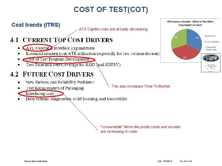
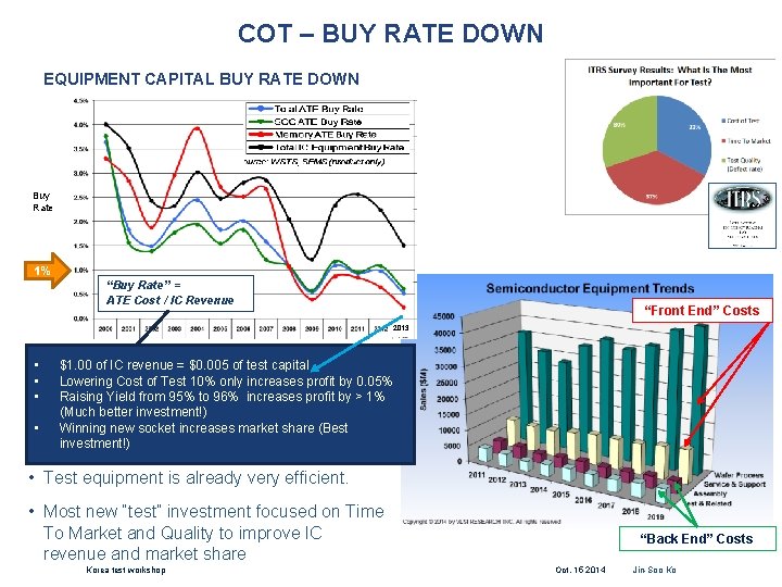
COST OF TEST(COT) Cost trends (ITRS) ATE Capital costs are actually decreasing This also increases Time To Market “consumable” items like probe cards and sockets are increasing in costs Korea test workshop Oct. 15 2014 Jin-Soo Ko

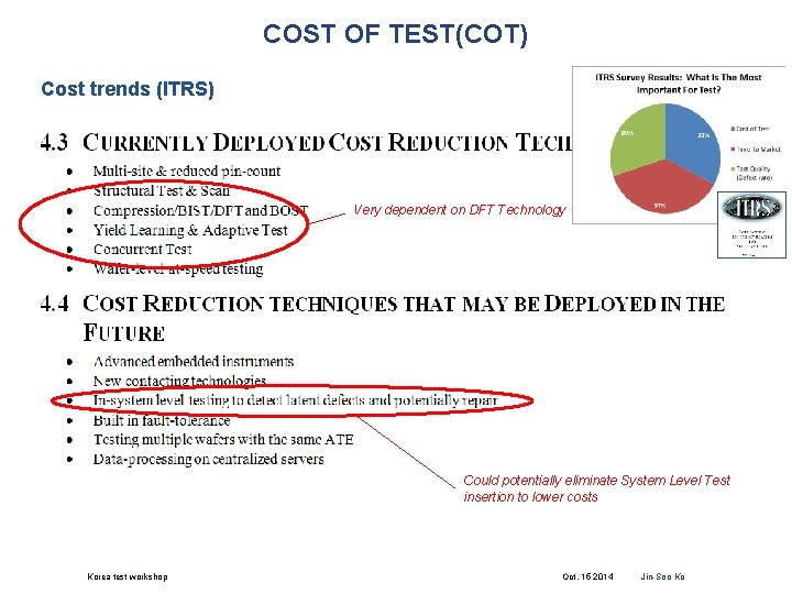
COST OF TEST(COT) Cost trends (ITRS) Very dependent on DFT Technology Could potentially eliminate System Level Test insertion to lower costs Korea test workshop Oct. 15 2014 Jin-Soo Ko

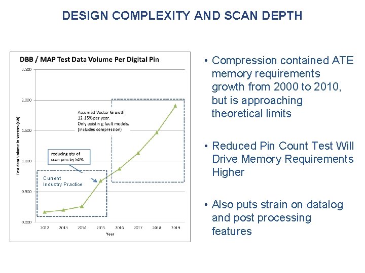
DESIGN COMPLEXITY AND SCAN DEPTH • Compression contained ATE memory requirements growth from 2000 to 2010, but is approaching theoretical limits Current Industry Practice • Reduced Pin Count Test Will Drive Memory Requirements Higher • Also puts strain on datalog and post processing features

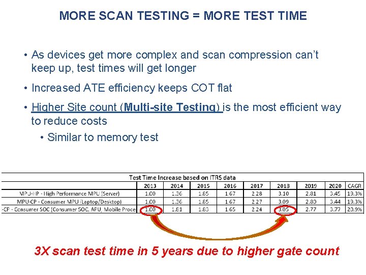
MORE SCAN TESTING = MORE TEST TIME • As devices get more complex and scan compression can’t keep up, test times will get longer • Increased ATE efficiency keeps COT flat • Higher Site count (Multi-site Testing) is the most efficient way to reduce costs • Similar to memory test 3 X scan test time in 5 years due to higher gate count

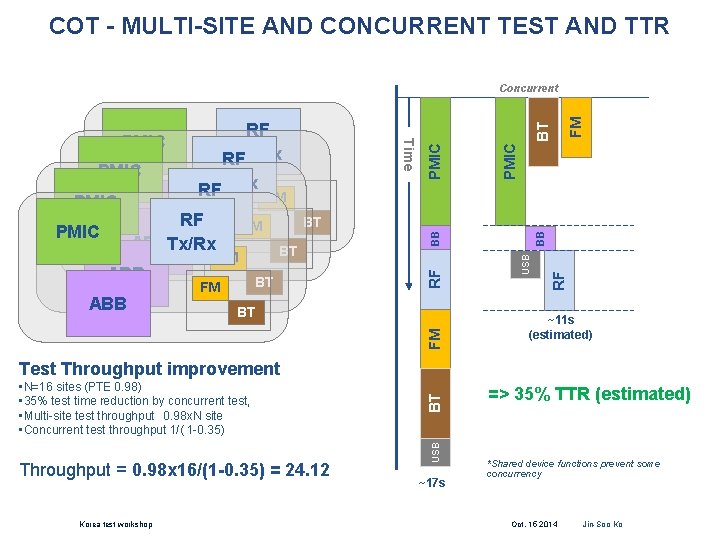
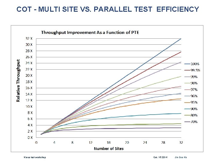
COT - MULTI-SITE AND CONCURRENT TEST AND TTR FM PMIC BT FM ABB BT FM RF ABB BT FM BB ABBTx/Rx BT FM USB PMIC FM BB PMIC Tx/Rx RF ABB Tx/Rx RF RF PMIC Time RF Tx/Rx RF PMIC BT Concurrent ~11 s (estimated) Throughput = 0. 98 x 16/(1 -0. 35) = 24. 12 Korea test workshop USB • N=16 sites (PTE 0. 98) • 35% test time reduction by concurrent test, • Multi-site test throughput 0. 98 x. N site • Concurrent test throughput 1/( 1 -0. 35) BT Test Throughput improvement ~17 s => 35% TTR (estimated) *Shared device functions prevent some concurrency Oct. 15 2014 Jin-Soo Ko

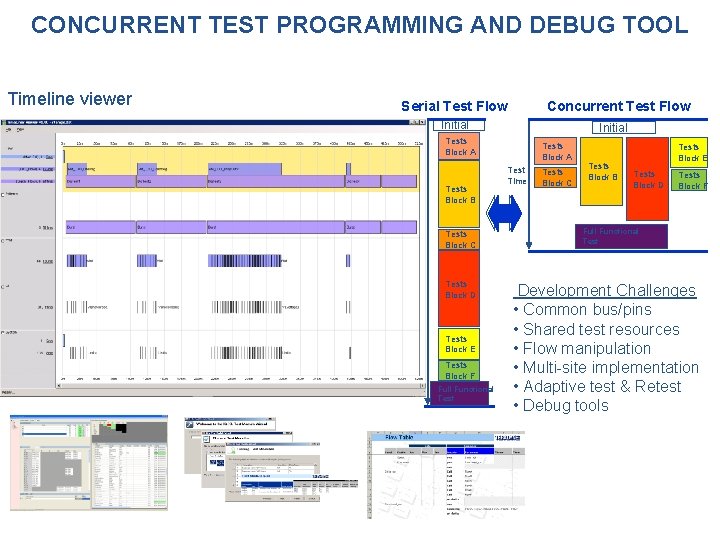
CONCURRENT TEST PROGRAMMING AND DEBUG TOOL Timeline viewer Concurrent Test Flow Serial Test Flow Initial Tests Block A Tests Block B Test Time Tests Block C Tests Block D Tests Block E Tests Block F Full Functional Tests Block A Test Time Tests Block C Tests Block B Tests Block E Tests Block D Tests Block F Full Functional Test Development Challenges • Common bus/pins • Shared test resources • Flow manipulation • Multi-site implementation • Adaptive test & Retest • Debug tools

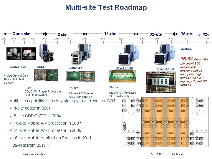
Multi-site Test Roadmap 2 or 4 -site 2000 2001 2002 16 -site 8 -site 2003 2004 2005 2006 2007 16 -site 32 -site 2009 2008 2010 2011 2012 2014 >> 32// 2016 TIU+DSA 16 -32 -site >1000 Catalyst/Tiger FLEX Ultra. FLEX-HC Ultra. FLEX-XD 4 -site Optical Disk Drive SOC test solution 8 -site CD, DVD Player Processor SOC test solution 16 -site 32 -site Mobile A/V Processor SOC test solution pin count SOC device test HIB design solution using new high density (x 2 ~ x 4) digital, AC, and DC options Multi-site capability is the key strategy to achieve low COT ü 4 -site codec in 2001 ü 8 -site CDP/DVDP in 2004 ü 16 -site Mobile A/V processor in 2007 ü 32 -site Mobile A/V processor in 2009 ü 16 -site Mobile Application Process in 2011 32 -siite from 2015 ? Korea test workshop Oct. 15 2014 Jin-Soo Ko 13

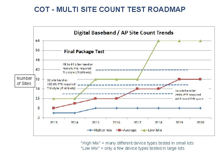
COT - MULTI SITE COUNT TEST ROADMAP Number of Sites “High Mix” = many different device types tested in small lots “Low Mix” = only a few device types tested in large lots

COT - MULTI SITE VS. PARALLEL TEST EFFICIENCY Korea test workshop Oct. 15 2014 Jin-Soo Ko

AWG SEQUENCE FOR PATTERN BASED PROGRAMMING q The entire AWG Plots BUCK 6 BUCK 2 BUCK 3 BUCK 4 BUCK 1 BUCK 5 BUCK 7 VIN LNR 1 LNR 2 LDR 1 LDR 2 LDR 3 MCU The scale reference is different in each plots. Korea test workshop Oct. 15 2014 Jin-Soo Ko

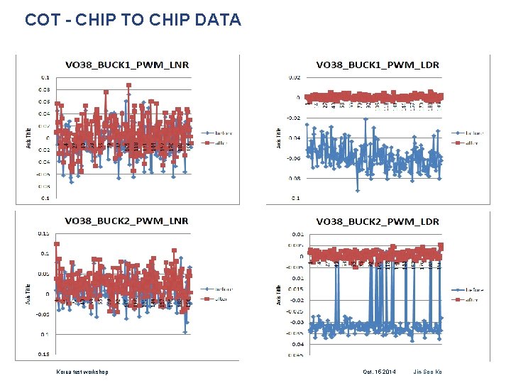
COT - CHIP TO CHIP DATA Korea test workshop Oct. 15 2014 Jin-Soo Ko

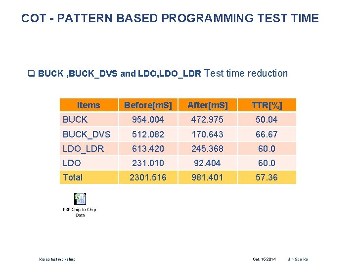
COT - PATTERN BASED PROGRAMMING TEST TIME q BUCK , BUCK_DVS and LDO, LDO_LDR Test time reduction Items Before[m. S] After[m. S] TTR[%] BUCK 954. 004 472. 975 50. 04 BUCK_DVS 512. 082 170. 643 66. 67 LDO_LDR 613. 420 245. 368 60. 0 LDO 231. 010 92. 404 60. 0 Total 2301. 516 981. 401 57. 36 Korea test workshop Oct. 15 2014 Jin-Soo Ko

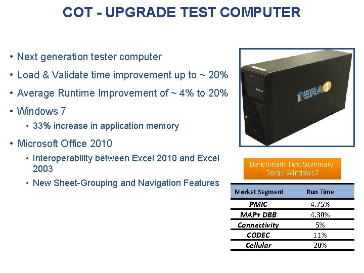
COT - UPGRADE TEST COMPUTER • Next generation tester computer • Load & Validate time improvement up to ~ 20% • Average Runtime Improvement of ~ 4% to 20% • Windows 7 • 33% increase in application memory • Microsoft Office 2010 • Interoperability between Excel 2010 and Excel 2003 • New Sheet-Grouping and Navigation Features Benchmark Test Summary: Tera 1 Windows 7 Market Segment Run Time PMIC MAP+ DBB Connectivity CODEC Cellular 4. 75% 4. 30% 5% 11% 20%

COT – BUY RATE DOWN EQUIPMENT CAPITAL BUY RATE DOWN Buy Rate 1% “Buy Rate” = ATE Cost / IC Revenue “Front End” Costs 2013 • • $1. 00 of IC revenue = $0. 005 of test capital Lowering Cost of Test 10% only increases profit by 0. 05% Raising Yield from 95% to 96% increases profit by > 1% (Much better investment!) Winning new socket increases market share (Best investment!) • Test equipment is already very efficient. • Most new “test” investment focused on Time To Market and Quality to improve IC revenue and market share Korea test workshop “Back End” Costs Oct. 15 2014 Jin-Soo Ko

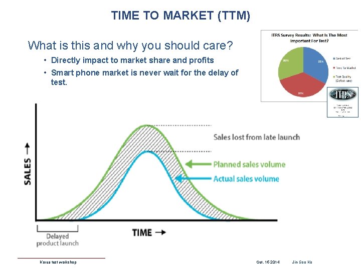
TIME TO MARKET (TTM) What is this and why you should care? • Directly impact to market share and profits • Smart phone market is never wait for the delay of test. Korea test workshop Oct. 15 2014 Jin-Soo Ko

TTM - HOW TO GET FAST TIME TO MARKET ? • Industry standard test system and SW capability • Integration with design and bench test • Advanced ATE SW tools for Time to Market Design Test Design Loop Failure Analysis / Yield Enhancement “on tester” tools Simulation Design “off tester” tools STDF • EDA Systems events ATPG • Timing/Levels • Mixed Signal • Repeatability • Correlation Pattern & Test program. Gen. transactions On-Tester Debug/ Characterization (hours/minutes) • ATPG Tools • Adaptive Test • Real-time Fault Isolation EDA-based Pattern Viewer • Simultaneous display of EDA and tester information • Diagnose Physical Device Faults Korea test workshop • Physical Failure Analysis • “Big Data” Storage Oct. 15 2014 Jin-Soo Ko

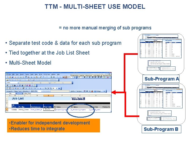
TTM - MULTI-SHEET USE MODEL = no more manual merging of sub programs • Separate test code & data for each sub program • Tied together at the Job List Sheet • Multi-Sheet Model Sub-Program A • Enabler for independent development • Reduces time to integrate Sub-Program B

TTM - RF TOOLS- LTE-A TX SIGNAL DEBUG TOOL IG-XL 7. 30 IG-XL 7. 40 • ESA 2. 0 • ESA 2. 5 3 GPP LTE Update TD-SCDMA Bluetooth 3. 0 802. 11 n 4 x 4 MIMO VSA 11 VSA 10. 01 • 1 port vector • Power de-embedding • Signal sheet support • Smith charting Korea test workshop IG-XL 8. 00. 01 IG-XL 8. 10 IG-XL 8. 20 • ESA 3. 0 LTE 8. 9 VSA 12 • ESA 3. 5 LTE-A (R 10) 802. 11 ac VSA 14 • ESA 4. 0 LTE-A (100 MHz) 802. 11 ac (160 MHz) 802. 11 ac (80+80) BT 4. 0 (LE) VSA 16 • 90% reduction in VSA instance creation times Oct. 15 2014 Jin-Soo Ko

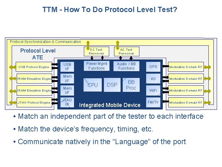
TTM - How To Do Protocol Level Test? Protocol Synchronization & Communication Protocol Level ATE USB Protocol Engine USB I/F DRAM Emulation Engine Mem I/F JTAG Protocol Engine JTAG I/F DC Test Resources AC Test Resources Power Mgmt Functions Audio / BB Functions CPU DSP BB Proc Integrated Mobile Device GPS Modulation Domain RF 4 G Modulation Domain RF Wi. Fi Modulation Domain RF FM/TV Modulation Domain RF • Match an independent part of the tester to each interface • Match the device’s frequency, timing, etc. • Communicate natively in the “Language” of the port

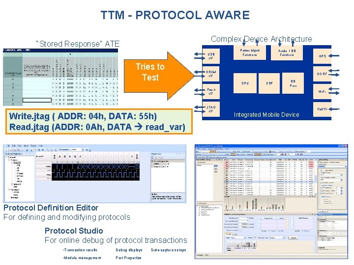
TTM - PROTOCOL AWARE Complex Device Architecture “Stored Response” ATE USB I/F Tries to Test Power Mgmt Functions Audio / BB Functions DRAM I/F 3 G RF CPU DSP BB Proc Flash I/F Write. jtag ( ADDR: 04 h, DATA: 55 h) Read. jtag (ADDR: 0 Ah, DATA read_var) Protocol Definition Editor For defining and modifying protocols Protocol Studio For online debug of protocol transactions • Transaction results Debug displays • Module management Port Properties Data capture setups JTAG I/F GPS Wi. Fi FM/TV Integrated Mobile Device

QUALITY OF TEST (QOT) – TECHNICAL CHALLENGES DEVICE TRENDS DRIVE NEW TEST NEEDS Lithography More scan testing with failure capture and diagnosis capability = More Patterns, especially at the start of the product life Mapping Physical and electrical defects Need to capture high volumes of scan data for offline analysis Higher speed Data IO High Speed Characterization capability with phenomenal Timing accuracy. Ability to use higher performance standard digital to screen devices in production to augment DFTOnly approach has more risk as data rates increase. Power Supply Stability Example Device Supplies < 700 m. V require excellent accuracy. Lower voltage Huge Current steps cannot cause glitches More complex Precise measurement of complex RF constellations RF Standards Larger number of RF measurements Device Reconfiguration More Complex Test Programs to do different testing per site New Packaging Ability to do a complete test at probe System Level Test capability for stacked die Test Flow Site 1 Site 2

QUALITY OF TEST (QOT) – TECHNICAL CHALLENGES DC CHALLENGES Korea test workshop Oct. 15 2014 Jin-Soo Ko

QOT - ITRS SEMICONDUCTOR ROADMAP FOR GATE LENGTH AND SUPPLY VOLTAGE • Supply Voltage levels will continue to decrease • New test requirements for power supplies to be stable and accurate • Need very critical DIB PI simulation and design process

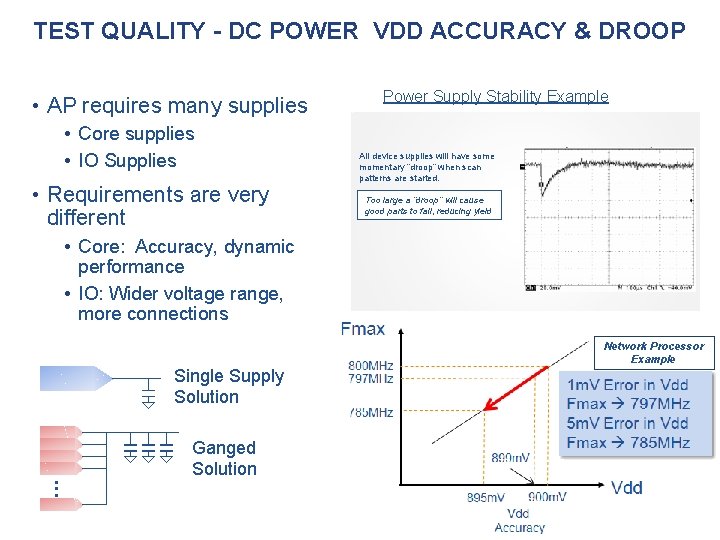
TEST QUALITY - DC POWER VDD ACCURACY & DROOP • AP requires many supplies • Core supplies • IO Supplies • Requirements are very different Power Supply Stability Example All device supplies will have some momentary “droop” when scan patterns are started. Too large a “droop” will cause good parts to fail, reducing yield • Core: Accuracy, dynamic performance • IO: Wider voltage range, more connections Single Supply Solution . . . Ganged Solution Network Processor Example

QUALITY OF TEST (QOT) – TECHNICAL CHALLENGES RF CHALLENGES Korea test workshop Oct. 15 2014 Jin-Soo Ko

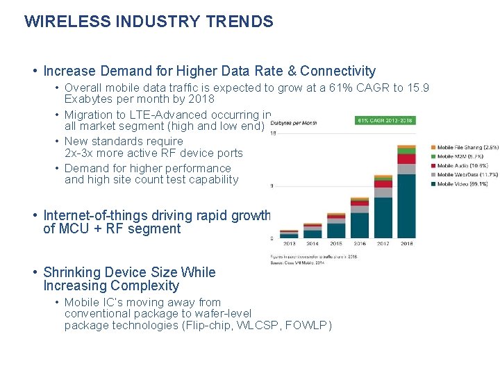
WIRELESS INDUSTRY TRENDS • Increase Demand for Higher Data Rate & Connectivity • Overall mobile data traffic is expected to grow at a 61% CAGR to 15. 9 Exabytes per month by 2018 • Migration to LTE-Advanced occurring in all market segment (high and low end) • New standards require 2 x-3 x more active RF device ports • Demand for higher performance and high site count test capability • Internet-of-things driving rapid growth of MCU + RF segment • Shrinking Device Size While Increasing Complexity • Mobile IC’s moving away from conventional package to wafer-level package technologies (Flip-chip, WLCSP, FOWLP)

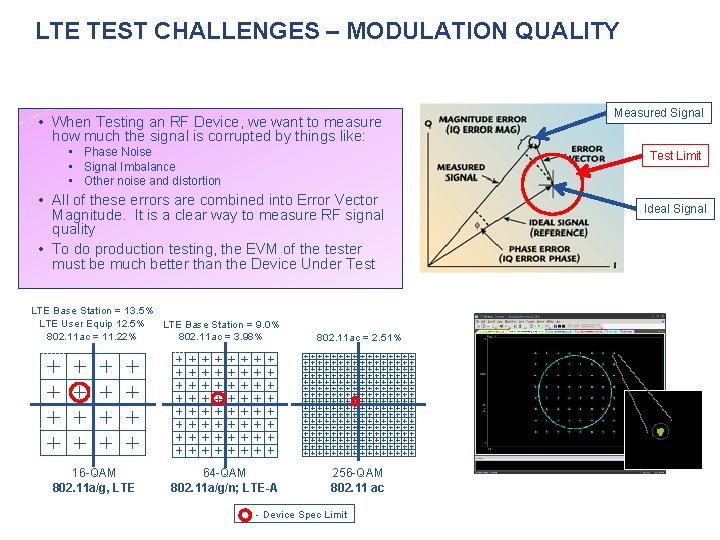
LTE TEST CHALLENGES – MODULATION QUALITY • When Testing an RF Device, we want to measure how much the signal is corrupted by things like: • Phase Noise • Signal Imbalance • Other noise and distortion Test Limit • All of these errors are combined into Error Vector Magnitude. It is a clear way to measure RF signal quality • To do production testing, the EVM of the tester must be much better than the Device Under Test LTE Base Station = 13. 5% LTE User Equip 12. 5% LTE Base Station = 9. 0% 802. 11 ac = 11. 22% 802. 11 ac = 3. 98% 16 -QAM 802. 11 a/g, LTE Measured Signal 64 -QAM 802. 11 a/g/n; LTE-A 802. 11 ac = 2. 51% 256 -QAM 802. 11 ac - Device Spec Limit Ideal Signal

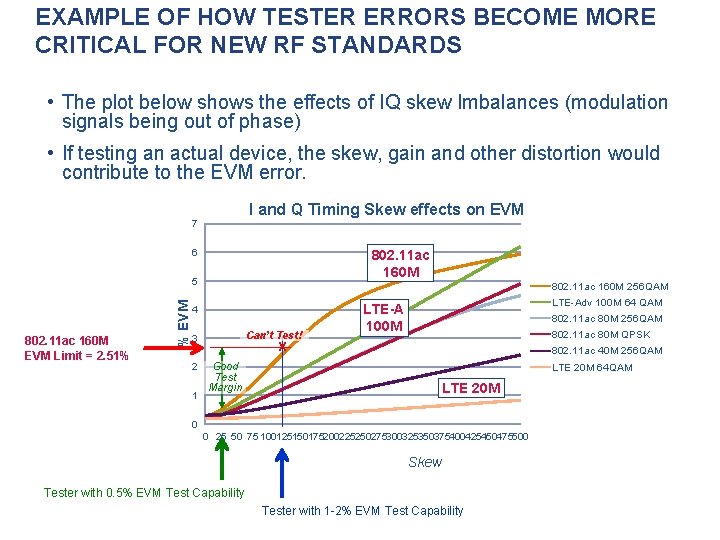
EXAMPLE OF HOW TESTER ERRORS BECOME MORE CRITICAL FOR NEW RF STANDARDS • The plot below shows the effects of IQ skew Imbalances (modulation signals being out of phase) • If testing an actual device, the skew, gain and other distortion would contribute to the EVM error. I and Q Timing Skew effects on EVM 7 6 802. 11 ac 160 M EVM Limit = 2. 51% % EVM 5 802. 11 ac 160 M 256 QAM 4 Can’t Test! 3 2 1 LTE-Adv 100 M 64 QAM LTE-A 100 M 802. 11 ac 80 M 256 QAM 802. 11 ac 80 M QPSK X Good Test Margin 802. 11 ac 40 M 256 QAM LTE 20 M 64 QAM LTE 20 M 0 0 25 50 75 100125150175200225250275300325350375400425450475500 Skew Tester with 0. 5% EVM Test Capability Tester with 1 -2% EVM Test Capability

QUALITY OF TEST (QOT) – TECHNICAL CHALLENGES HIGH SPEED INTERFACE CHALLENGES Korea test workshop Oct. 15 2014 Jin-Soo Ko

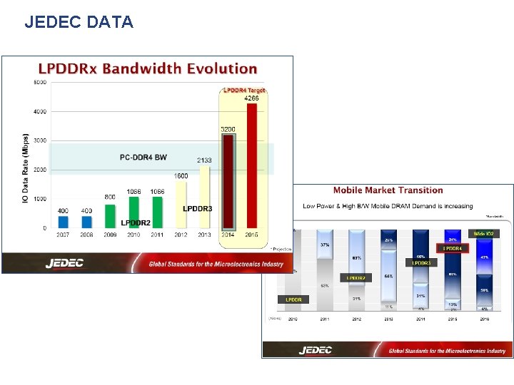
JEDEC DATA

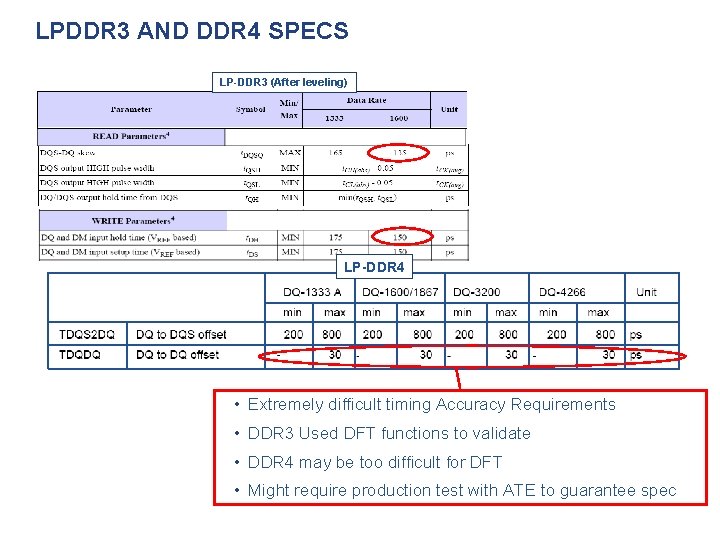
LPDDR 3 AND DDR 4 SPECS LP-DDR 3 (After leveling) LP-DDR 4 • Extremely difficult timing Accuracy Requirements • DDR 3 Used DFT functions to validate • DDR 4 may be too difficult for DFT • Might require production test with ATE to guarantee spec

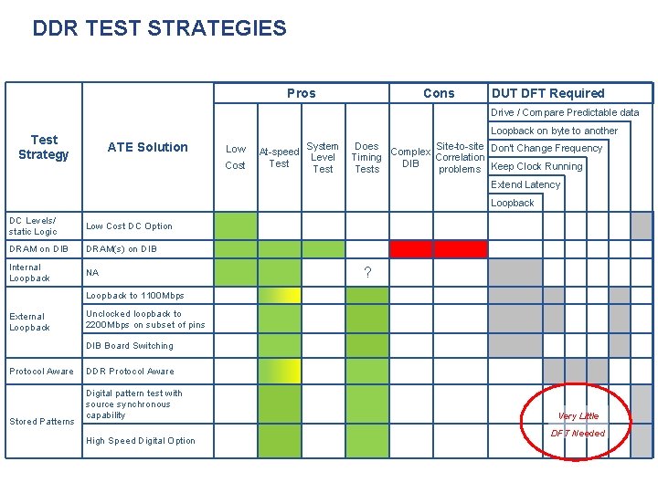
DDR TEST STRATEGIES Pros Cons DUT DFT Required Drive / Compare Predictable data Loopback on byte to another Test Strategy ATE Solution Low Cost At-speed Test System Level Test Does Site-to-site Don’t Change Frequency Complex Timing Correlation DIB Tests problems Keep Clock Running Extend Latency Loopback DC Levels/ static Logic Low Cost DC Option DRAM on DIB DRAM(s) on DIB Internal Loopback NA ? Loopback to 1100 Mbps External Loopback Unclocked loopback to 2200 Mbps on subset of pins DIB Board Switching Protocol Aware Stored Patterns DDR Protocol Aware Digital pattern test with source synchronous capability High Speed Digital Option Very Little DFT Needed

HIGH SPEED SERIAL TEST • High Speed Serial Challenges • Maintain signal integrity from Instrument to DUT • Support rapid increases in serial data rates ITRS Data Rate Forecast • 2013: 16 Gbps • 2014: 28+Gbps • 2015: 45 Gbps / Multi. Level • Minimize tester capital investment • Maximize tester capital useful life • Test Strategy • Support high pin count interfaces with standard tester instrument • Develop Re-useable IP than can be implemented on DIBs or DIB modules • Deliver solutions as • Turnkey applications • Vendor-designed and manufactured hardware only • Custom hardware made by ATE vendor, 3 rd Party or Hi. Silicon (under license) Advantages • No need to buy new Tester Options – much lower cost • Minimizes signal path to DUT for best signal quality and device yield • Simplifies DIB by eliminating matching circuitry • Can be customized easily

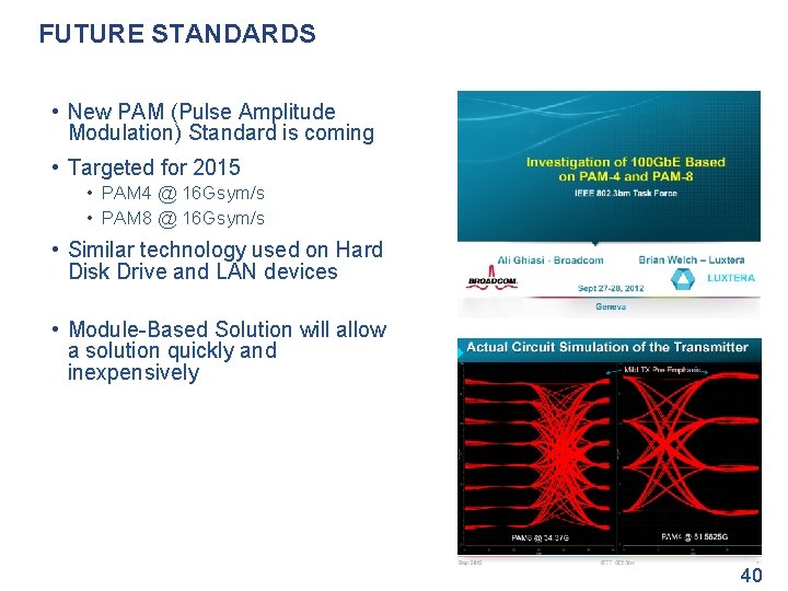
FUTURE STANDARDS • New PAM (Pulse Amplitude Modulation) Standard is coming • Targeted for 2015 • PAM 4 @ 16 Gsym/s • PAM 8 @ 16 Gsym/s • Similar technology used on Hard Disk Drive and LAN devices • Module-Based Solution will allow a solution quickly and inexpensively 40

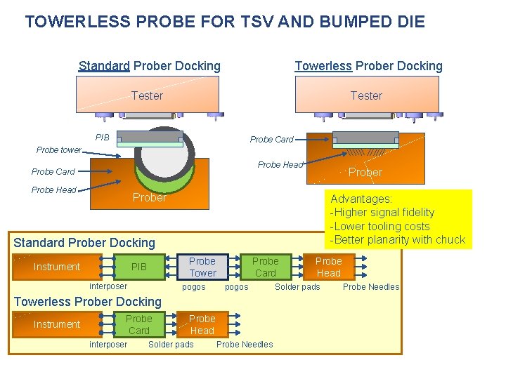
TOWERLESS PROBE FOR TSV AND BUMPED DIE Standard Prober Docking Towerless Prober Docking Tester PIB Probe Card Probe tower Probe Head Probe Card Probe Head Prober Advantages: -Higher signal fidelity -Lower tooling costs -Better planarity with chuck Standard Prober Docking Instrument Probe Tower PIB interposer pogos Probe Card pogos Towerless Prober Docking Instrument Probe Card interposer Probe Head Solder pads Probe Needles

CONCLUSION • Cost of Test ATE Capital Program development Multisite and Concurrent test Pattern Oriented Test DFT dependent test solutions • Time To Market SW and debugging tools Adaptive testing Protocol Aware • Test Quality DC accuracy and power RF AC speed and skew High speed IO Direct Wafer Probing Korea test workshop Oct. 15 2014 Jin-Soo Ko

Q&A Jin-Soo Ko Highbrand building 10’th floor, Yang. Ja, Seo. Cho, Seoul Korea Jin-Soo. Ko@Teradyne. com