Future evolution of the Fast Trac Ker FTK


- Slides: 29

Future evolution of the Fast Trac. Ker (FTK) processing unit C. Gentsos, Aristotle University of Thessaloniki FTK 324318 FP 7 -PEOPLE-2012 -IAPP FTK executive board 21/7/2014 1

Presentation Overview Key Fast Trac. Ker (FTK) components � Goal of my work � FPGA firmware � FPGA Device utilization and power � System latency and processing speed � Progress � 2

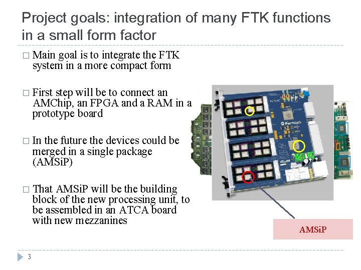
Project goals: integration of many FTK functions in a small form factor � Main goal is to integrate the FTK system in a more compact form � First step will be to connect an AMChip, an FPGA and a RAM in a prototype board � In the future the devices could be merged in a single package (AMSi. P) � That AMSi. P will be the building block of the new processing unit, to be assembled in an ATCA board with new mezzanines 3 AMSi. P

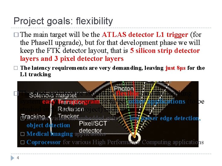
Project goals: flexibility � The main target will be the ATLAS detector L 1 trigger (for the Phase. II upgrade), but for that development phase we will keep the FTK detector layout, that is 5 silicon strip detector layers and 3 pixel detector layers � The latency requirements are very demanding, leaving just 8μs for the L 1 tracking � The final architecture should be flexible, and the resulting system easy to reprogram to target other applications (to be studied in the IAPP project) such as: Machine vision for embedded systems: low power edge detection, object detection � Medical imaging applications � Coprocessor for various High Performance Computing applications � 4

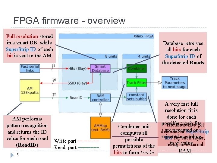
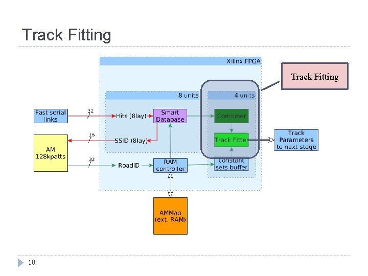
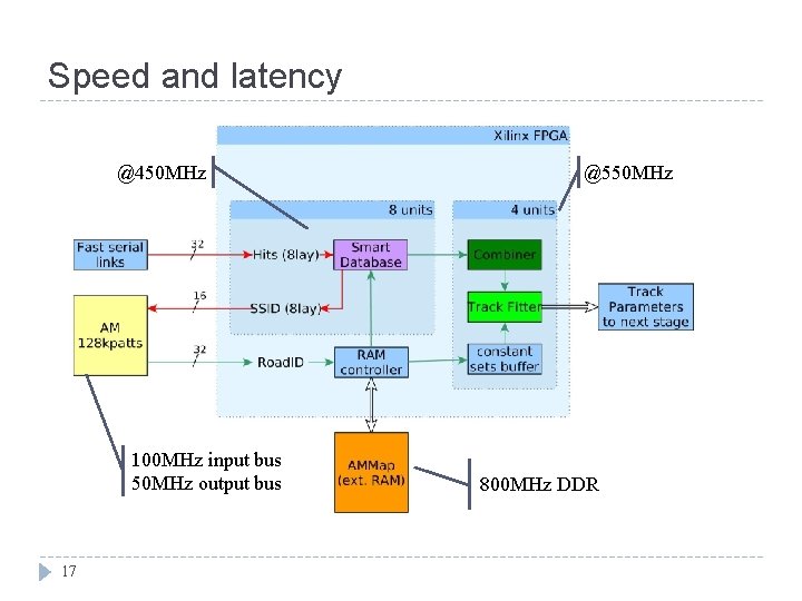
FPGA firmware - overview Full resolution stored in a smart DB, while Super. Strip ID of each hit is sent to the AM AM performs pattern recognition and returns the ID value for each road (Road. ID) 5 Database retreives all hits for each Super. Strip ID of the detected Roads Write part −−−−−−− Read part −−−−−−− Combiner unit computes all possible permutations of the hits to form tracks A very fast full resolution fit is done for each possible track, fits The Road. IDs get are accepted or decoded to Super. Strip rejected IDs foraccording each layer, 2 to χ an value using external RAM

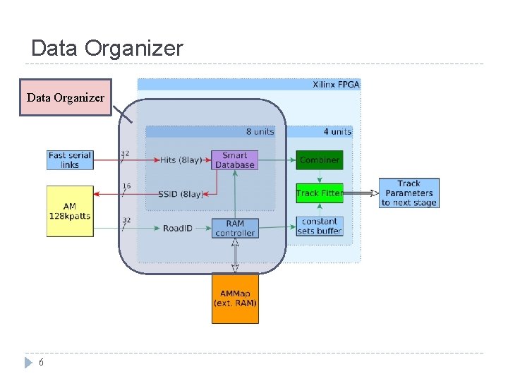
Data Organizer 6

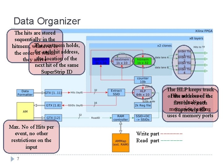
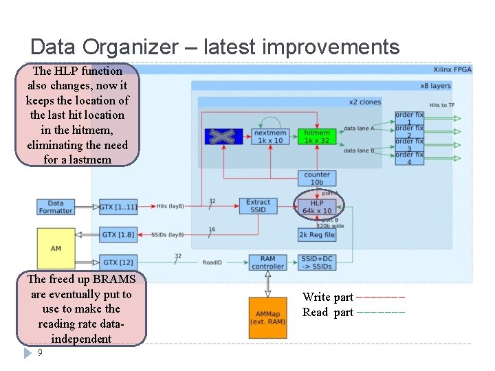
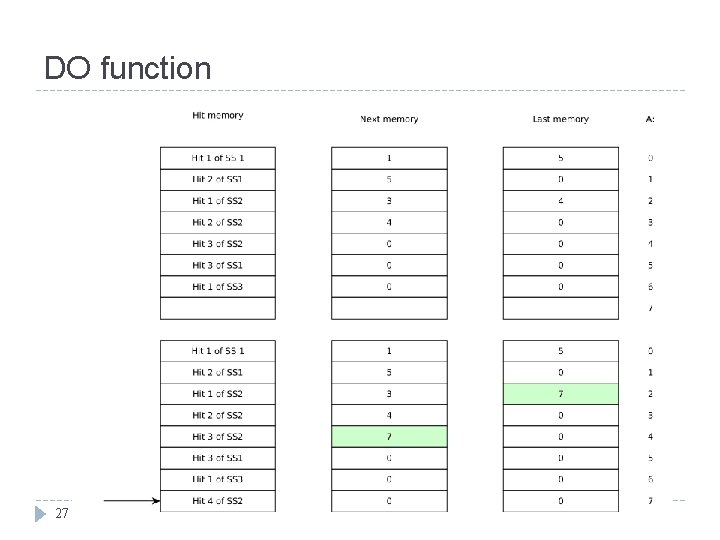
Data Organizer The hits are stored sequentially in the The nextmem holds, hitmem, whatever is each hit address, the orderfor in which the location of they arrive next hit of the same Super. Strip ID The HLP keeps track cloned of. Hits the are address of in the twohit dual-port first of each memories, reading Super. Strip ID uses 4 memory ports Max. No of Hits per event, no other restrictions on the input 7 Write part −−−−−−− Read part −−−−−−−

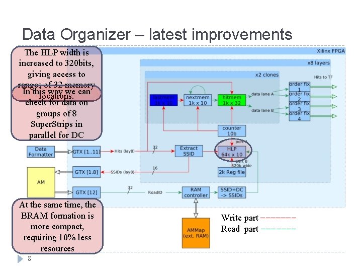
Data Organizer – latest improvements The HLP width is increased to 320 bits, giving access to ranges of 32 memory In this way we can locations. check for data on groups of 8 Super. Strips in parallel for DC At the same time, the BRAM formation is more compact, requiring 10% less resources 8 Write part −−−−−−− Read part −−−−−−−

Data Organizer – latest improvements The HLP function also changes, now it keeps the location of the last hit location in the hitmem, eliminating the need for a lastmem The freed up BRAMS are eventually put to use to make the reading rate dataindependent 9 Write part −−−−−−− Read part −−−−−−−

Track Fitting 10

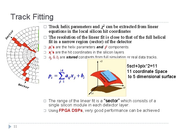
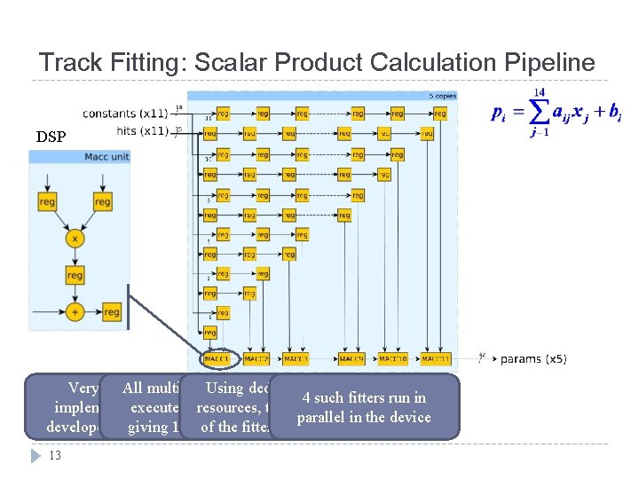
Track Fitting � � � Track helix parameters and 2 can be extracted from linear equations in the local silicon hit coordinates The resolution of the linear fit is close to that of the full helical fit in a narrow region (sector) of the detector pi’s are the helix parameters and 2 components. xj’s are the hit coordinates in the silicon layers. aij & bi are stored constants from full simulation or real data tracks. 5 sct+3 pix*2=11 11 coordinate Space to 5 dimensional surface � � 11 The range of the linear fit is a “sector” which consists of a single silicon module in each detector layer. Using FPGA DSPs, very good performance can be achieved

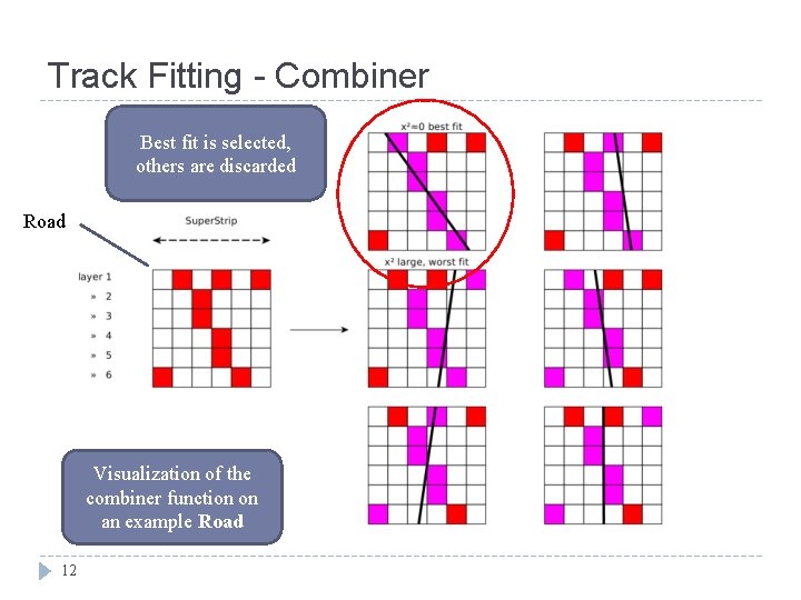
Track Fitting - Combiner Best fit is selected, others are discarded Road Visualization of the combiner function on an example Road 12

Track Fitting: Scalar Product Calculation Pipeline DSP Very fast. All FPGA multiplications Using are dedicated DSP 4 such fitters run in implementation executed was inresources, parallel, the frequency parallel in the device developed forgiving the fitter 1 fit of perthe clock fitter is 550 MHz 13

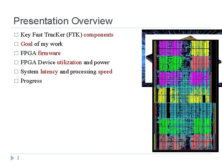
FPGA implementation � The main components of the design have already been implemented � Placement on the device has been made for estimating true achievable clock rates and the power dissipation � Target device is 28 nm, Xilinx 7 -series XC 7 K 325 T-900 ffg -3 � The clock frequencies we are targeting are close to the actual limits of the device � To achieve such clock rates, many coding guidelines and advanced design techniques must be followed 14

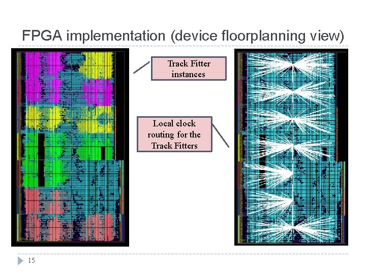
FPGA implementation (device floorplanning view) Track Fitter instances Local clock routing for the Track Fitters 15

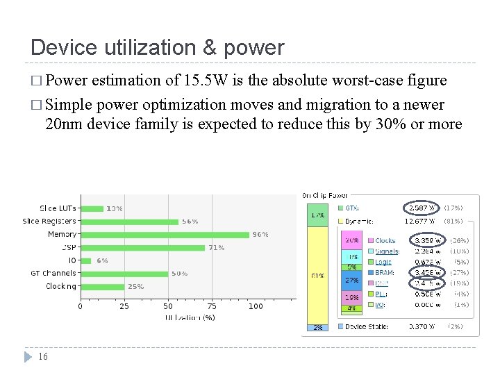
Device utilization & power � Power estimation of 15. 5 W is the absolute worst-case figure � Simple power optimization moves and migration to a newer 20 nm device family is expected to reduce this by 30% or more 16

Speed and latency @450 MHz 100 MHz input bus 50 MHz output bus 17 @550 MHz 800 MHz DDR

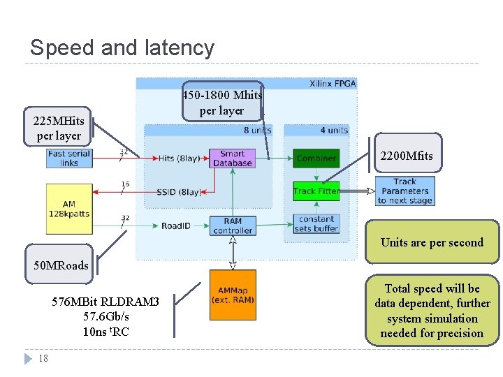
Speed and latency 225 MHits per layer 450 -1800 Mhits per layer 2200 Mfits Units are per second 50 MRoads 576 MBit RLDRAM 3 57. 6 Gb/s 10 ns t. RC 18 Total speed will be data dependent, further system simulation needed for precision

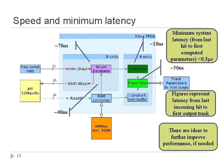
Speed and minimum latency ~70 ns ~10 ns Minimum system latency (from last hit to first computed parameters) <0. 3μs ~50 ns ~40 ns Figures represent latency from last incoming hit to first output track There are ideas to further improve performance, if needed 19

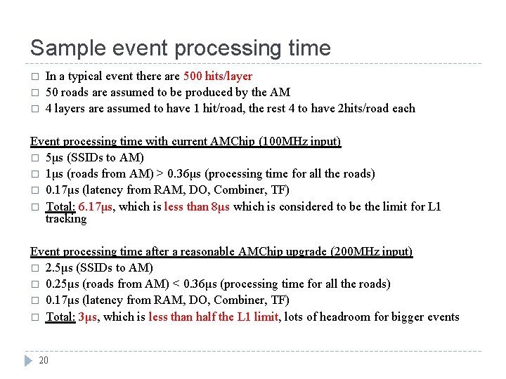
Sample event processing time � � � In a typical event there are 500 hits/layer 50 roads are assumed to be produced by the AM 4 layers are assumed to have 1 hit/road, the rest 4 to have 2 hits/road each Event processing time with current AMChip (100 MHz input) � 5μs (SSIDs to AM) � 1μs (roads from AM) > 0. 36μs (processing time for all the roads) � 0. 17μs (latency from RAM, DO, Combiner, TF) � Total: 6. 17μs, which is less than 8μs which is considered to be the limit for L 1 tracking Event processing time after a reasonable AMChip upgrade (200 MHz input) � 2. 5μs (SSIDs to AM) � 0. 25μs (roads from AM) < 0. 36μs (processing time for all the roads) � 0. 17μs (latency from RAM, DO, Combiner, TF) � Total: 3μs, which is less than half the L 1 limit, lots of headroom for bigger events 20

Progress � Data organizer and Track Fitter already implemented in the FPGA device � After the last improvements on the Data Organizer are over, the combiner and external memory interface will be implemented � Speed and latency figures of the system are promising � After design completion, testing on the prototype board will follow 21

Thank you! 22

Backup � Backup 23 slides, way more to be added

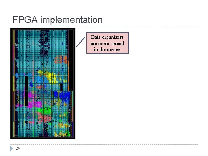
FPGA implementation Data organizers are more spread in the device 24

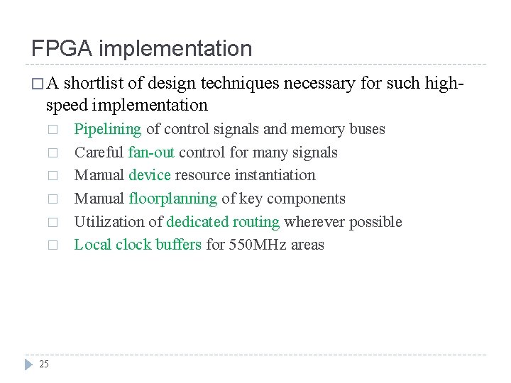
FPGA implementation �A shortlist of design techniques necessary for such highspeed implementation � � � 25 Pipelining of control signals and memory buses Careful fan-out control for many signals Manual device resource instantiation Manual floorplanning of key components Utilization of dedicated routing wherever possible Local clock buffers for 550 MHz areas

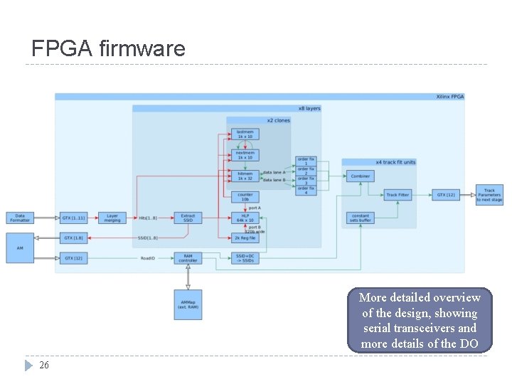
FPGA firmware More detailed overview of the design, showing serial transceivers and more details of the DO 26

DO function 27

Latency, processing speed � To write 1 k hits to the DO, 4. 5 us is needed � To forward 100 roads worth of hits to the Track Fitter another ~0. 5 -1. 5 us is necessary (data dependent) � The TF itself because of its high operating frequency does not have any noticeable latency, the maximum processing speed would be close to 2. 4 Gfits/sec if it was utilized 100% of the event time � There are ideas on how to increase all those numbers if there is need � Simulations will be done to show if the current performance is enough 28

Latency, processing speed � There are ideas on how to increase all those numbers if there is need � Just migrating to an Ultra. Scale device can increase the performance, by utilizing even more parallelism and clock rate capabilities � Simulations have to be done to show if the current performance is enough, but the figures seem good for now 29