Fundamentals of MOSFETs u MOS Capacitor fundamentals u
- Slides: 69

Fundamentals of MOSFETs u MOS Capacitor fundamentals u Device Structure u Visualization of various phases MOSFET operation u Id-Vd Characteristics u Id-Vg Characteristics u Important device parameters MOS Device Physics and Designs 1 Instructor: Pei-Wen Li Dept. of E. E. NCU

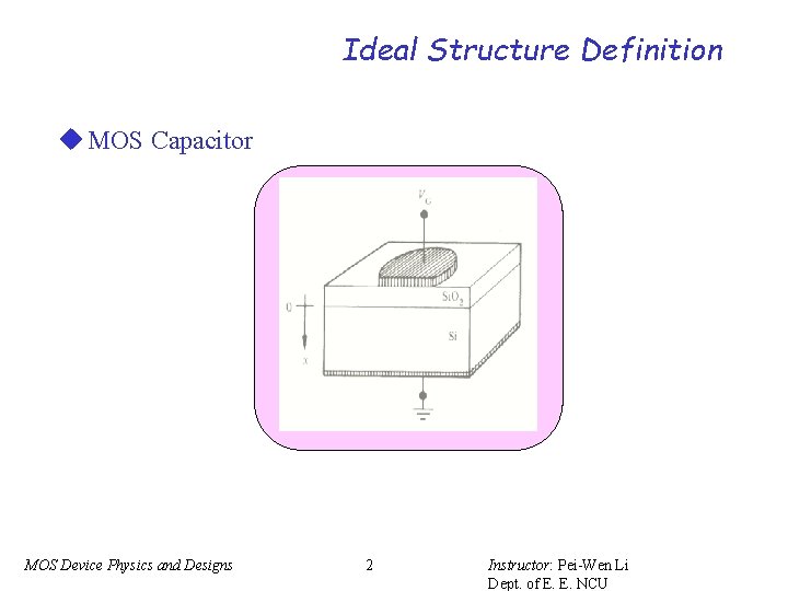
Ideal Structure Definition u MOS Capacitor MOS Device Physics and Designs 2 Instructor: Pei-Wen Li Dept. of E. E. NCU

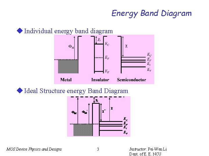
Energy Band Diagram u Individual energy band diagram u Ideal Structure energy Band Diagram MOS Device Physics and Designs 3 Instructor: Pei-Wen Li Dept. of E. E. NCU

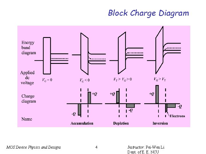
Block Charge Diagram MOS Device Physics and Designs 4 Instructor: Pei-Wen Li Dept. of E. E. NCU

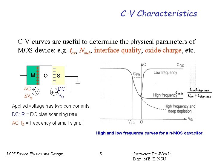
C-V Characteristics C-V curves are useful to determine the physical parameters of MOS device: e. g. tox, Nsub, interface quality, oxide charge, etc. ++++++ M AC Vg O + S DC VG Applied voltage has two components: DC: R = DC bias scanning rate AC: f. S = frequency of small signal High and low frequency curves for a n-MOS capacitor. MOS Device Physics and Designs 5 Instructor: Pei-Wen Li Dept. of E. E. NCU

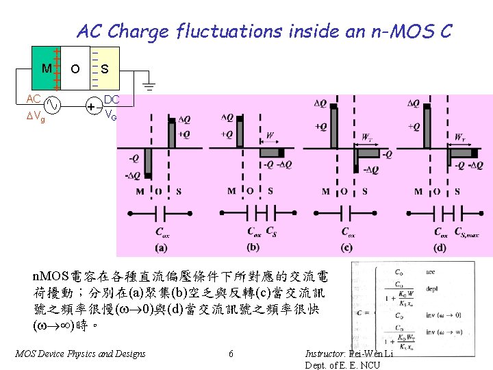
AC Charge fluctuations inside an n-MOS C ++++++ M AC Vg O + S DC VG n. MOS電容在各種直流偏壓條件下所對應的交流電 荷擾動;分別在(a)聚集(b)空乏與反轉(c)當交流訊 號之頻率很慢(w 0)與(d)當交流訊號之頻率很快 (w )時。 MOS Device Physics and Designs 6 Instructor: Pei-Wen Li Dept. of E. E. NCU

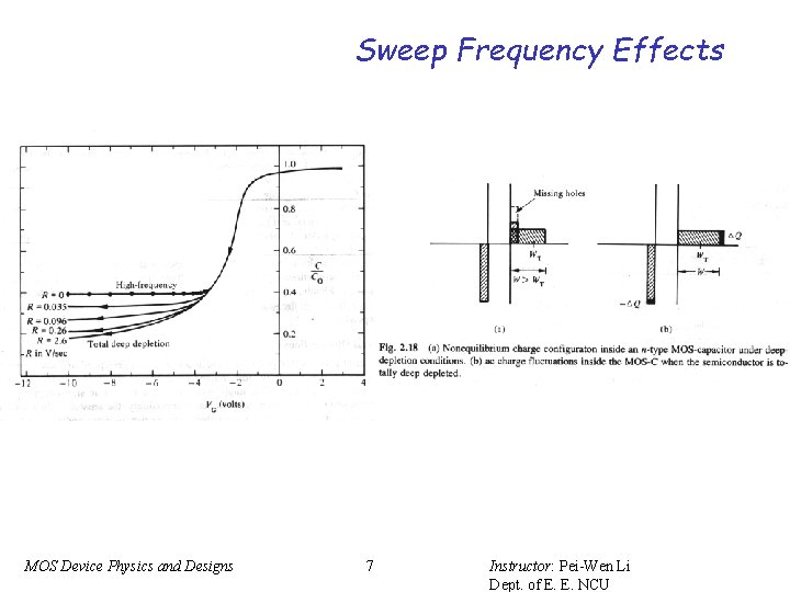
Sweep Frequency Effects MOS Device Physics and Designs 7 Instructor: Pei-Wen Li Dept. of E. E. NCU

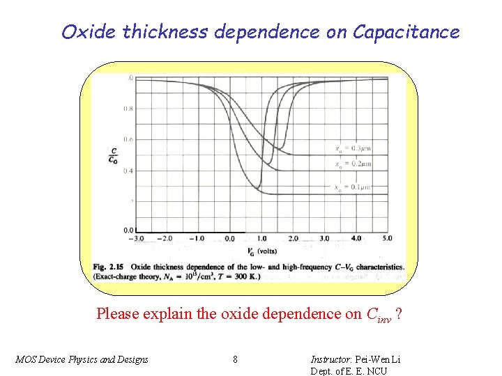
Oxide thickness dependence on Capacitance Please explain the oxide dependence on Cinv ? MOS Device Physics and Designs 8 Instructor: Pei-Wen Li Dept. of E. E. NCU

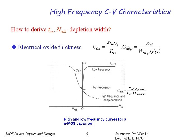
High Frequency C-V Characteristics How to derive tox, Nsub, depletion width? u Electrical oxide thickness High and low frequency curves for a n-MOS capacitor. MOS Device Physics and Designs 9 Instructor: Pei-Wen Li Dept. of E. E. NCU

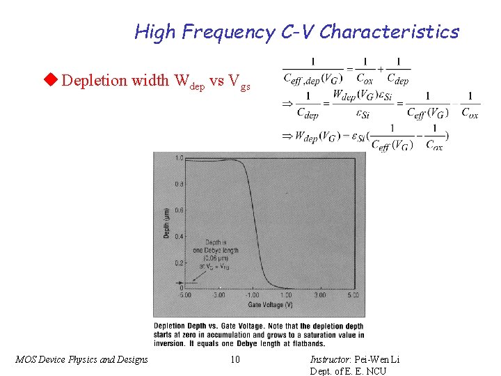
High Frequency C-V Characteristics u Depletion width Wdep vs Vgs MOS Device Physics and Designs 10 Instructor: Pei-Wen Li Dept. of E. E. NCU

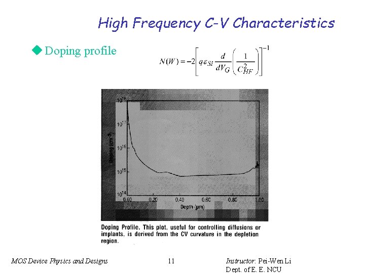
High Frequency C-V Characteristics u Doping profile MOS Device Physics and Designs 11 Instructor: Pei-Wen Li Dept. of E. E. NCU

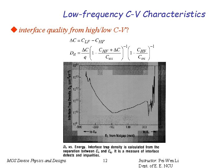
Low-frequency C-V Characteristics u interface quality from high/low C-V? MOS Device Physics and Designs 12 Instructor: Pei-Wen Li Dept. of E. E. NCU

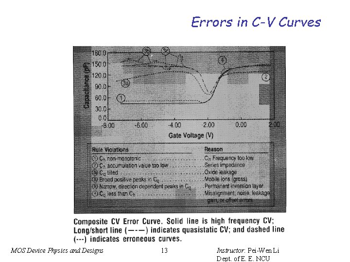
Errors in C-V Curves MOS Device Physics and Designs 13 Instructor: Pei-Wen Li Dept. of E. E. NCU

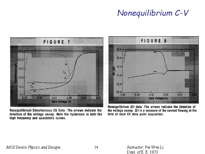
Nonequilibrium C-V MOS Device Physics and Designs 14 Instructor: Pei-Wen Li Dept. of E. E. NCU

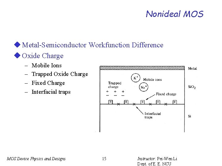
Nonideal MOS u Metal-Semiconductor Workfunction Difference u Oxide Charge – – Mobile Ions Trapped Oxide Charge Fixed Charge Interfacial traps MOS Device Physics and Designs 15 Instructor: Pei-Wen Li Dept. of E. E. NCU

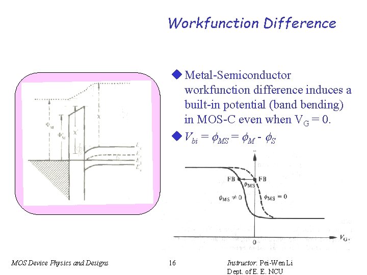
Workfunction Difference u Metal-Semiconductor workfunction difference induces a built-in potential (band bending) in MOS-C even when VG = 0. u Vbi = MS = M - S MOS Device Physics and Designs 16 Instructor: Pei-Wen Li Dept. of E. E. NCU

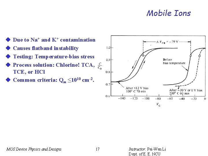
Mobile Ions u u Due to Na+ and K+ contamination Causes flatband instability Testing: Temperature-bias stress Process solution: Chlorine! TCA, TCE, or HCl u Common criteria: Qm ≤ 1010 cm-2. MOS Device Physics and Designs 17 Instructor: Pei-Wen Li Dept. of E. E. NCU

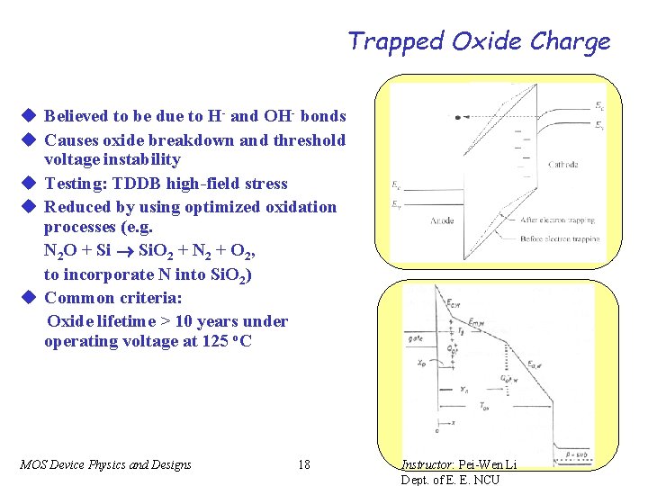
Trapped Oxide Charge u Believed to be due to H- and OH- bonds u Causes oxide breakdown and threshold voltage instability u Testing: TDDB high-field stress u Reduced by using optimized oxidation processes (e. g. N 2 O + Si Si. O 2 + N 2 + O 2, to incorporate N into Si. O 2) u Common criteria: Oxide lifetime > 10 years under operating voltage at 125 o. C MOS Device Physics and Designs 18 Instructor: Pei-Wen Li Dept. of E. E. NCU

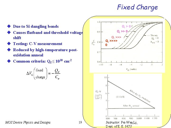
Fixed Charge u Due to Si dangling bonds u Causes flatband threshold voltage shift u Testing: C-V measurement u Reduced by high-temperature postoxidation anneal u Common criteria: Qf ≤ 1010 cm-2 MOS Device Physics and Designs 19 Qf > 0 Qf >>>> 0 0 Instructor: Pei-Wen Li Dept. of E. E. NCU

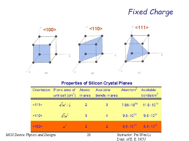
Fixed Charge <100> <111> <110> Properties of Silicon Crystal Planes MOS Device Physics and Designs 20 Instructor: Pei-Wen Li Dept. of E. E. NCU

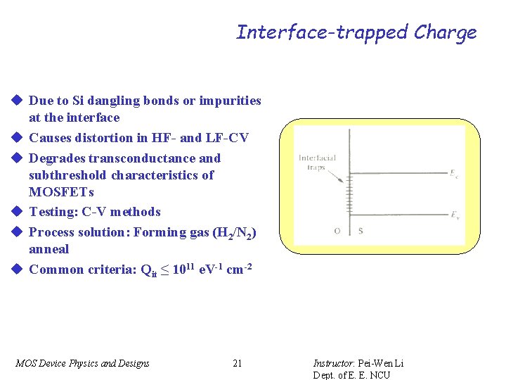
Interface-trapped Charge u Due to Si dangling bonds or impurities at the interface u Causes distortion in HF- and LF-CV u Degrades transconductance and subthreshold characteristics of MOSFETs u Testing: C-V methods u Process solution: Forming gas (H 2/N 2) anneal u Common criteria: Qit ≤ 1011 e. V-1 cm-2 MOS Device Physics and Designs 21 Instructor: Pei-Wen Li Dept. of E. E. NCU

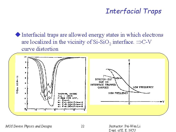
Interfacial Traps u Interfacial traps are allowed energy states in which electrons are localized in the vicinity of Si-Si. O 2 interface. C-V curve distortion MOS Device Physics and Designs 22 Instructor: Pei-Wen Li Dept. of E. E. NCU

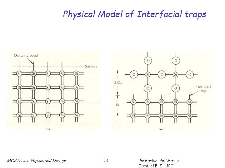
Physical Model of Interfacial traps MOS Device Physics and Designs 23 Instructor: Pei-Wen Li Dept. of E. E. NCU

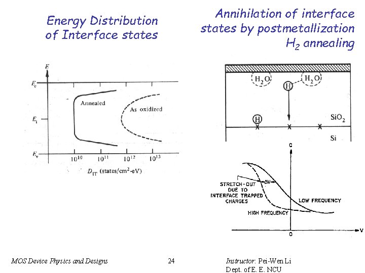
Annihilation of interface states by postmetallization H 2 annealing Energy Distribution of Interface states MOS Device Physics and Designs 24 Instructor: Pei-Wen Li Dept. of E. E. NCU

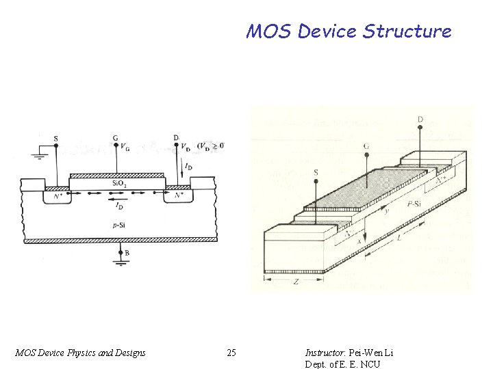
MOS Device Structure MOS Device Physics and Designs 25 Instructor: Pei-Wen Li Dept. of E. E. NCU

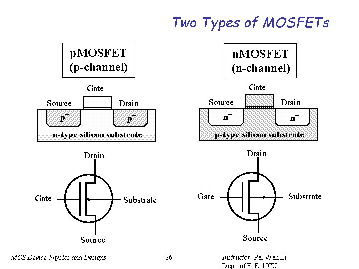
Two Types of MOSFETs p. MOSFET (p-channel) n. MOSFET (n-channel) Gate Source Drain p+ Source Drain n+ n+ p+ n-type silicon substrate p-type silicon substrate Drain Gate Substrate Source MOS Device Physics and Designs Substrate 26 Instructor: Pei-Wen Li Dept. of E. E. NCU

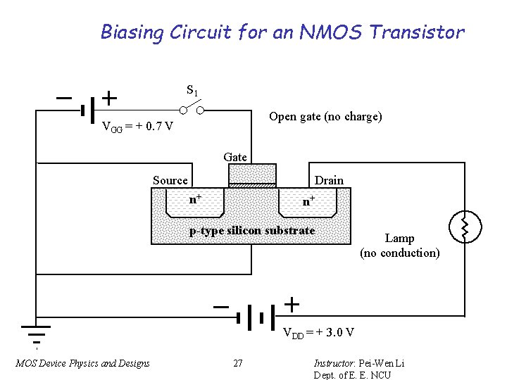
Biasing Circuit for an NMOS Transistor S 1 Open gate (no charge) VGG = + 0. 7 V Gate Source Drain n+ n+ p-type silicon substrate Lamp (no conduction) VDD = + 3. 0 V MOS Device Physics and Designs 27 Instructor: Pei-Wen Li Dept. of E. E. NCU

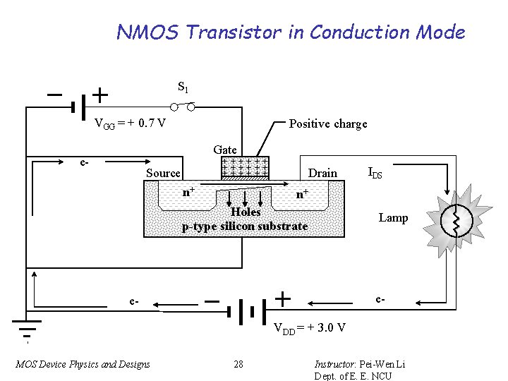
NMOS Transistor in Conduction Mode S 1 VGG = + 0. 7 V Positive charge Gate e- ++++++ Source n+ Drain IDS n+ Holes p-type silicon substrate Lamp e- e. VDD = + 3. 0 V MOS Device Physics and Designs 28 Instructor: Pei-Wen Li Dept. of E. E. NCU

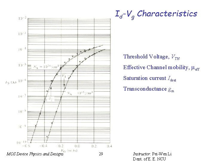
Id-Vg Characteristics Threshold Voltage, VTH Effective Channel mobility, meff Saturation current Idsat Transconductance gm MOS Device Physics and Designs 29 Instructor: Pei-Wen Li Dept. of E. E. NCU

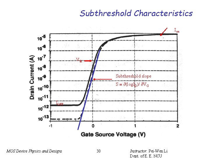
Subthreshold Characteristics Ion Vth Subthreshold slope S (log. ID)/ VG IOFF MOS Device Physics and Designs 30 Instructor: Pei-Wen Li Dept. of E. E. NCU

Subthreshold Characteristics u Threshold voltage could be determined by – Cut-in voltage from Linear I-V – Maximum gm – Constant current criteria MOS Device Physics and Designs 31 Instructor: Pei-Wen Li Dept. of E. E. NCU

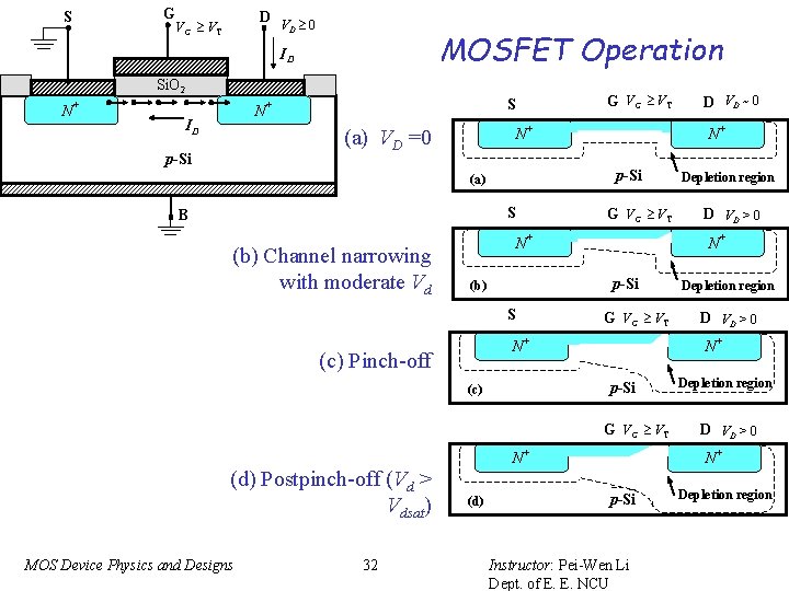
S G D V 0 D VG V T MOSFET Operation ID Si. O 2 N+ S N+ ID N++ N (a) VD =0 p-Si S B G VG V T N++ N S G VG V T N++ N (c) Pinch-off G VG V T (d) Postpinch-off (Vd > Vdsat) MOS Device Physics and Designs 32 N++ N (d) D VD > 0 Depletion region D VD > 0 N+ p-Si (c) Depletion region N+ N+ p-Si (b) D VD ~ 0 N++ N p-Si (a) (b) Channel narrowing with moderate Vd G VG V T Depletion region D VD > 0 N+ p-Si Instructor: Pei-Wen Li Dept. of E. E. NCU Depletion region

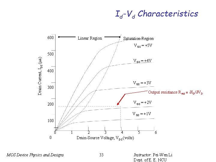
Id-Vd Characteristics 600 Linear Region Saturation Region VGS = +5 V Drain Current, IDS (ma) 500 VGS = +4 V 400 VGS = +3 V 300 Output resistance Rout ID/ VD VGS = +2 V 200 VGS = +1 V 100 0 0 MOS Device Physics and Designs 1 2 3 4 5 Drain-Source Voltage, VDS (volts) 33 6 Instructor: Pei-Wen Li Dept. of E. E. NCU

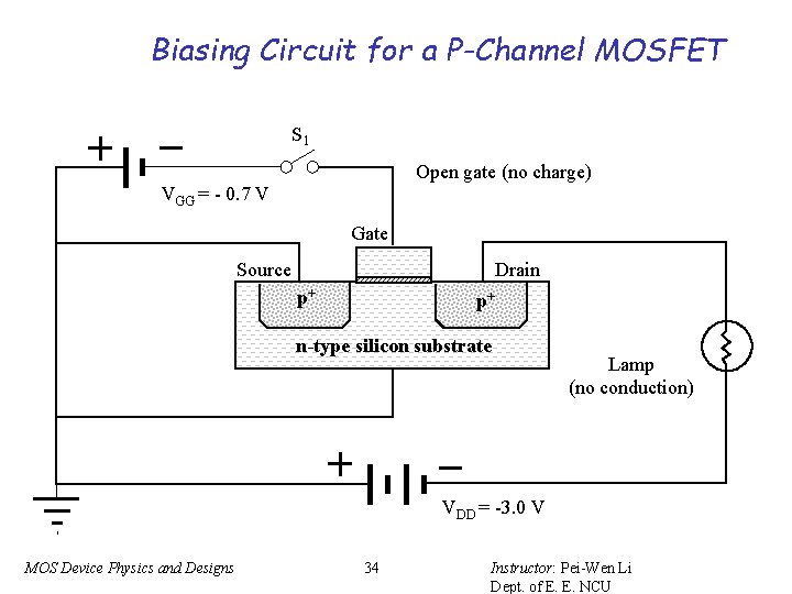
Biasing Circuit for a P-Channel MOSFET S 1 Open gate (no charge) VGG = - 0. 7 V Gate Source Drain p+ p+ n-type silicon substrate Lamp (no conduction) VDD = -3. 0 V MOS Device Physics and Designs 34 Instructor: Pei-Wen Li Dept. of E. E. NCU

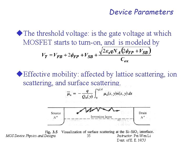
Device Parameters u. The threshold voltage: is the gate voltage at which MOSFET starts to turn-on, and is modeled by u. Effective mobility: affected by lattice scattering, ion scattering, and surface scattering. MOS Device Physics and Designs 35 Instructor: Pei-Wen Li Dept. of E. E. NCU

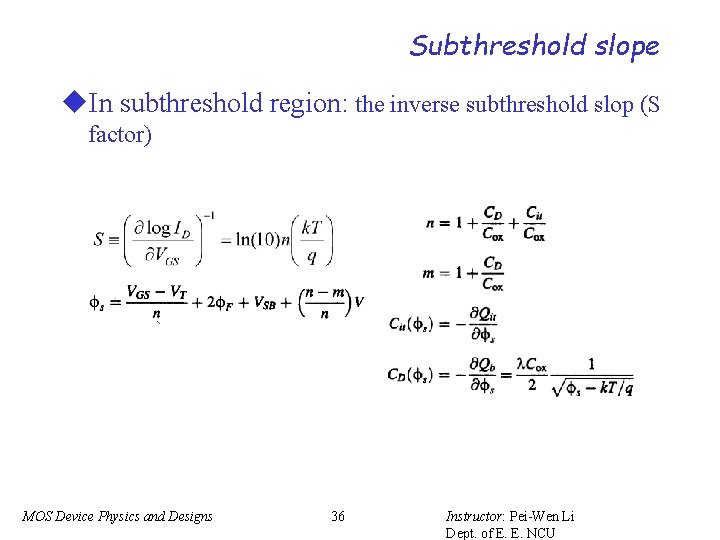
Subthreshold slope u. In subthreshold region: the inverse subthreshold slop (S factor) MOS Device Physics and Designs 36 Instructor: Pei-Wen Li Dept. of E. E. NCU

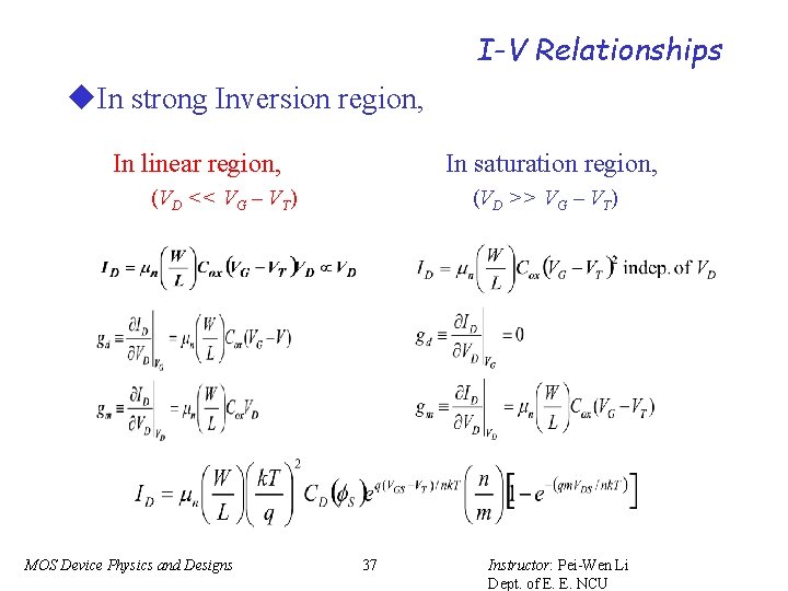
I-V Relationships u. In strong Inversion region, In linear region, In saturation region, (VD << VG – VT) MOS Device Physics and Designs (VD >> VG – VT) 37 Instructor: Pei-Wen Li Dept. of E. E. NCU

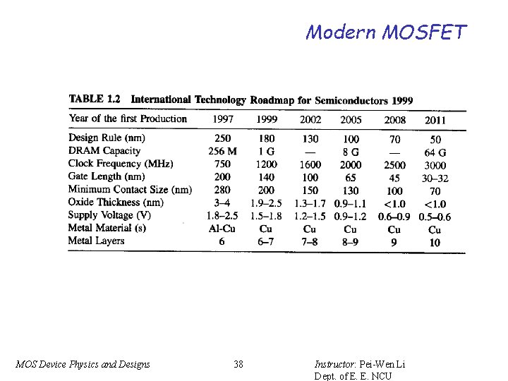
Modern MOSFET MOS Device Physics and Designs 38 Instructor: Pei-Wen Li Dept. of E. E. NCU

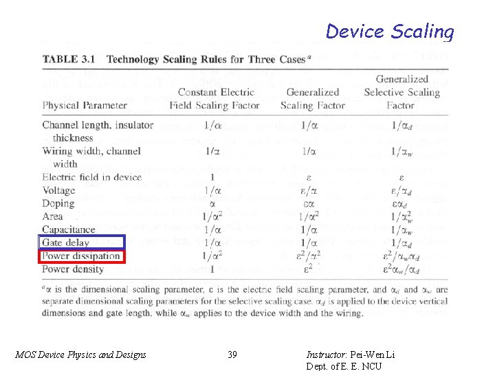
Device Scaling MOS Device Physics and Designs 39 Instructor: Pei-Wen Li Dept. of E. E. NCU

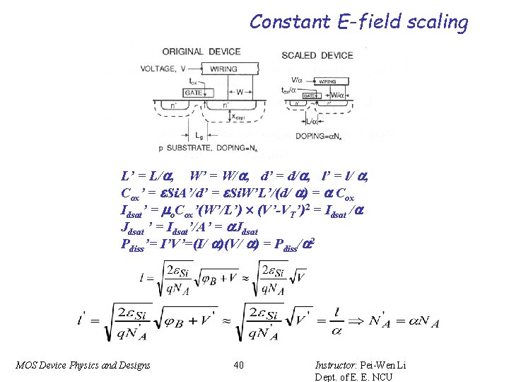
Constant E-field scaling L’ = L/ , W’ = W/ , d’ = d/ , l’ = l/ , Cox’ = Si. A’/d’ = Si. W’L’/(d/ ) = Cox Idsat’ = mo. Cox’(W’/L’) (V’-VT’)2 = Idsat / Jdsat ’ = Idsat’/A’ = Jdsat Pdiss’= I’V’=(I/ )(V/ ) = Pdiss/ 2 MOS Device Physics and Designs 40 Instructor: Pei-Wen Li Dept. of E. E. NCU

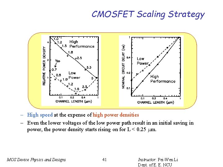
CMOSFET Scaling Strategy – High speed at the expense of high power densities – Even the lower voltages of the low power path result in an initial saving in power, the power density starts rising on for L < 0. 25 mm. MOS Device Physics and Designs 41 Instructor: Pei-Wen Li Dept. of E. E. NCU

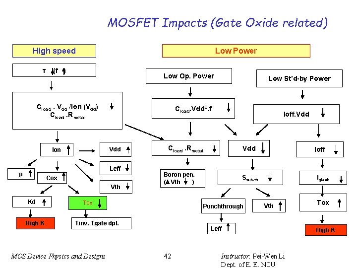
MOSFET Impacts (Gate Oxide related) High speed τ Low Power (f ) Low Op. Power Cload. Vdd /Ion (Vdd) Cload. Rmetal Cload. Vdd 2. f Vdd Ion Leff μ Cox Vth Kd High K Ioff. Vdd Cload. Rmetal Vdd Boron pen. ( Vth ) Tox Ioff Ssub-th Punchthrough Tinv. Tgate dpl. MOS Device Physics and Designs Low St’d-by Power Igleak Vth Leff 42 Instructor: Pei-Wen Li Dept. of E. E. NCU Tox High K

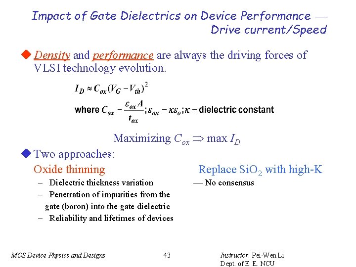
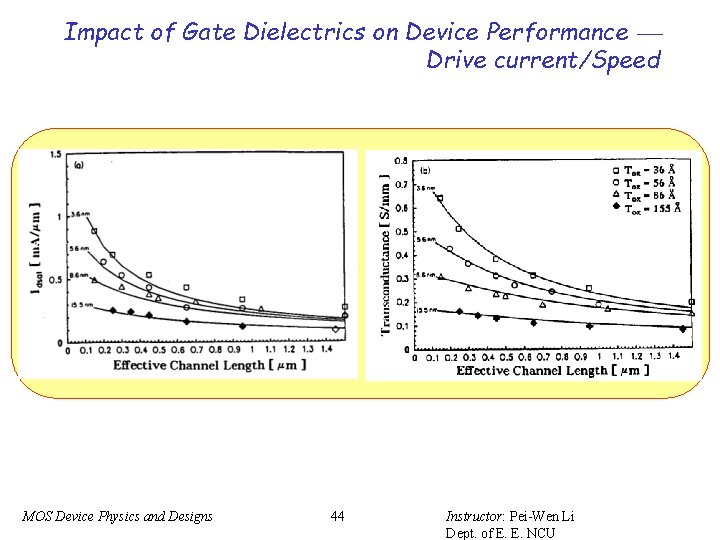
Impact of Gate Dielectrics on Device Performance Drive current/Speed u Density and performance are always the driving forces of VLSI technology evolution. Maximizing Cox max ID u Two approaches: Oxide thinning Replace Si. O 2 with high-K – Dielectric thickness variation – Penetration of impurities from the gate (boron) into the gate dielectric – Reliability and lifetimes of devices MOS Device Physics and Designs 43 No consensus Instructor: Pei-Wen Li Dept. of E. E. NCU

Impact of Gate Dielectrics on Device Performance Drive current/Speed MOS Device Physics and Designs 44 Instructor: Pei-Wen Li Dept. of E. E. NCU

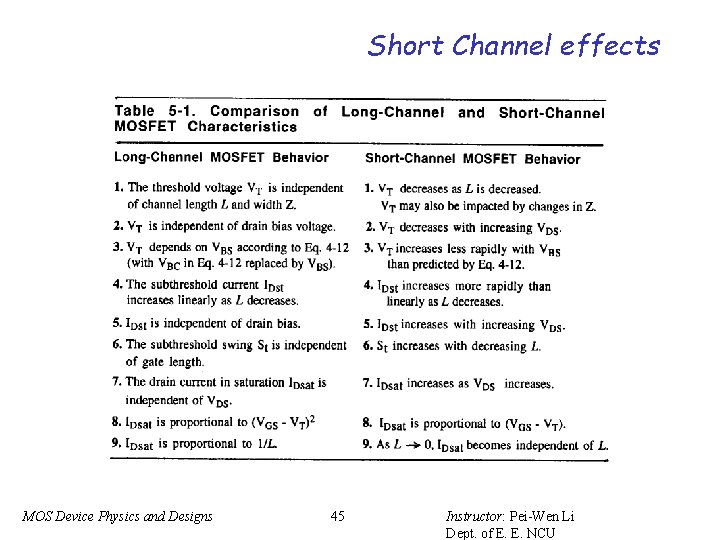
Short Channel effects MOS Device Physics and Designs 45 Instructor: Pei-Wen Li Dept. of E. E. NCU

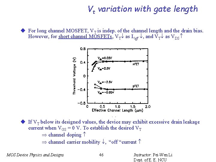
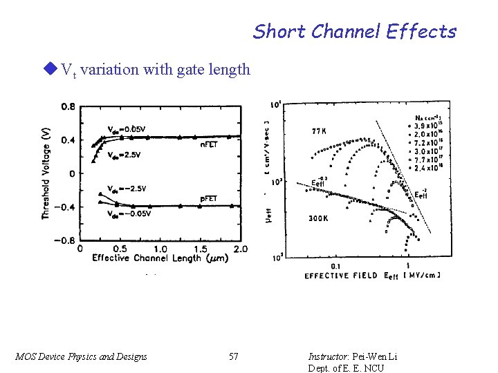
Vt variation with gate length u For long channel MOSFET, VT is indep. of the channel length and the drain bias. However, for short channel MOSFETs, VT as Leff , and VT as VDS u If VT below its designed values, the device may exhibit excessive drain leakage current when VGS = 0 V. To establish the desired VT channel doping channel carrier mobility , “off “current MOS Device Physics and Designs 46 Instructor: Pei-Wen Li Dept. of E. E. NCU

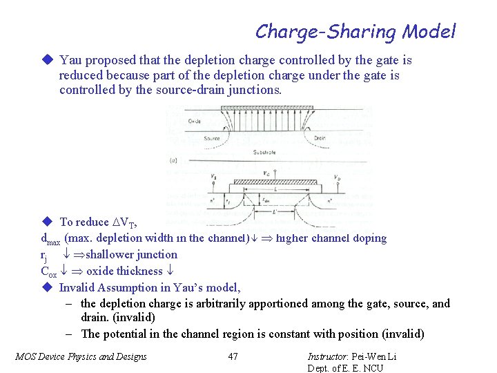
Charge-Sharing Model u Yau proposed that the depletion charge controlled by the gate is reduced because part of the depletion charge under the gate is controlled by the source-drain junctions. u To reduce VT, dmax (max. depletion width in the channel) higher channel doping rj shallower junction Cox oxide thickness u Invalid Assumption in Yau’s model, – the depletion charge is arbitrarily apportioned among the gate, source, and drain. (invalid) – The potential in the channel region is constant with position (invalid) MOS Device Physics and Designs 47 Instructor: Pei-Wen Li Dept. of E. E. NCU

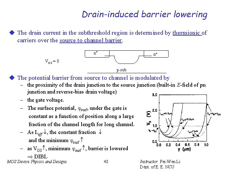
Drain-induced barrier lowering u The drain current in the subthreshold region is determined by thermionic of carriers over the source to channel barrier. n+ n+ VDS = 0 p-sub u The potential barrier from source to channel is modulated by – the proximity of the drain junction to the source junction (built-in E-field of pn junction and reverse-bias drain voltage) – the gate voltage. – The surface potential, surf, under the gate is constant as a function of position along a large fraction of the channel length for long channel. – As Leff , the constant fraction and the minimum surf – as VDS , minimum surf , barrier is lowered DIBL MOS Device Physics and Designs 48 Instructor: Pei-Wen Li Dept. of E. E. NCU

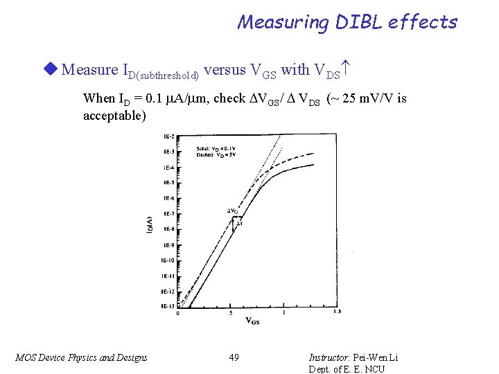
Measuring DIBL effects u Measure ID(subthreshold) versus VGS with VDS When ID = 0. 1 m. A/mm, check VGS/ VDS (~ 25 m. V/V is acceptable) MOS Device Physics and Designs 49 Instructor: Pei-Wen Li Dept. of E. E. NCU

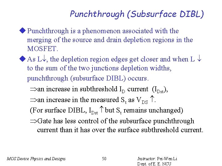
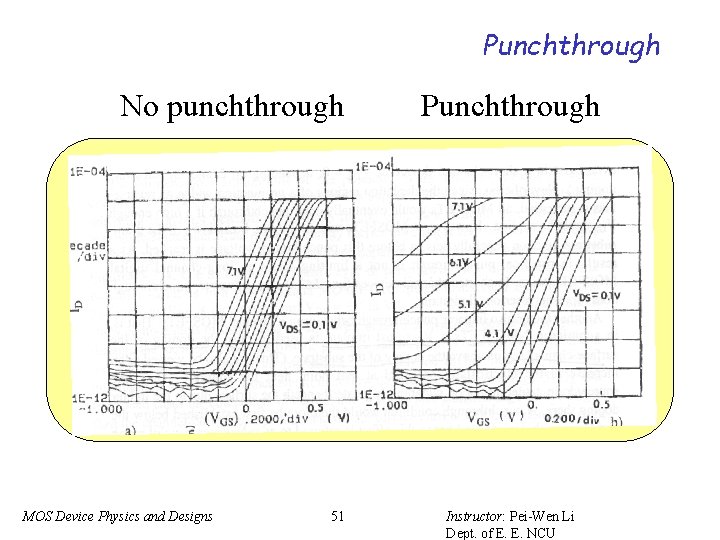
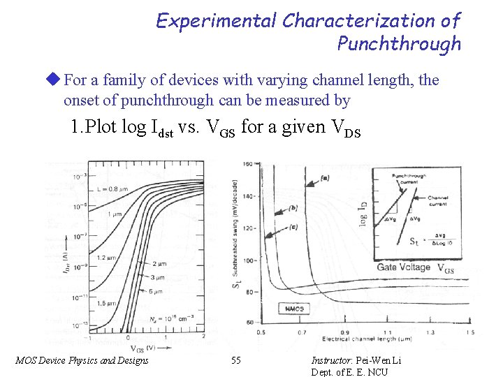
Punchthrough (Subsurface DIBL) u Punchthrough is a phenomenon associated with the merging of the source and drain depletion regions in the MOSFET. u As L , the depletion region edges get closer and when L to the sum of the two junctions depletion widths, punchthrough (subsurface DIBL) occurs. an increase in subthreshold ID current (IDst), an increase in the measured St as VDS . (For surface DIBL, IDst but St remains unchanged) Gate has less control of the subsurface punchthrough current than it has over the surface subthreshold current. MOS Device Physics and Designs 50 Instructor: Pei-Wen Li Dept. of E. E. NCU

Punchthrough No punchthrough MOS Device Physics and Designs 51 Punchthrough Instructor: Pei-Wen Li Dept. of E. E. NCU

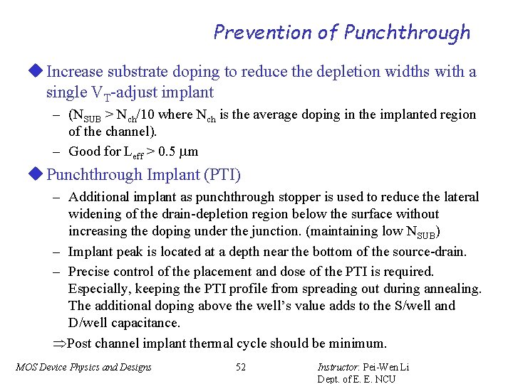
Prevention of Punchthrough u Increase substrate doping to reduce the depletion widths with a single VT-adjust implant – (NSUB > Nch/10 where Nch is the average doping in the implanted region of the channel). – Good for Leff > 0. 5 mm u Punchthrough Implant (PTI) – Additional implant as punchthrough stopper is used to reduce the lateral widening of the drain-depletion region below the surface without increasing the doping under the junction. (maintaining low NSUB) – Implant peak is located at a depth near the bottom of the source-drain. – Precise control of the placement and dose of the PTI is required. Especially, keeping the PTI profile from spreading out during annealing. The additional doping above the well’s value adds to the S/well and D/well capacitance. Post channel implant thermal cycle should be minimum. MOS Device Physics and Designs 52 Instructor: Pei-Wen Li Dept. of E. E. NCU

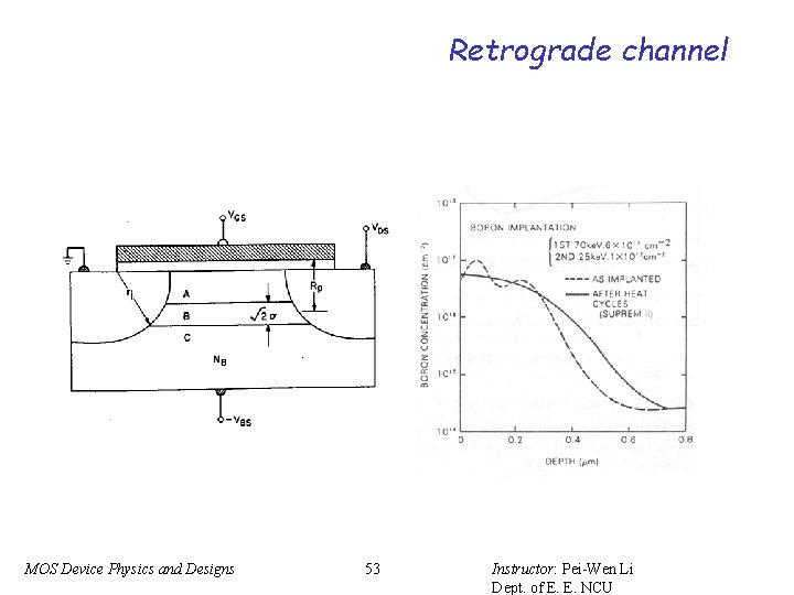
Retrograde channel MOS Device Physics and Designs 53 Instructor: Pei-Wen Li Dept. of E. E. NCU

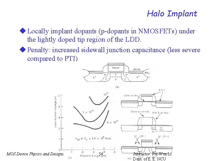
Halo Implant u Locally implant dopants (p-dopants in NMOSFETs) under the lightly doped tip region of the LDD. u Penalty: increased sidewall junction capacitance (less severe compared to PTI) MOS Device Physics and Designs 54 Instructor: Pei-Wen Li Dept. of E. E. NCU

Experimental Characterization of Punchthrough u For a family of devices with varying channel length, the onset of punchthrough can be measured by 1. Plot log Idst vs. VGS for a given VDS MOS Device Physics and Designs 55 Instructor: Pei-Wen Li Dept. of E. E. NCU

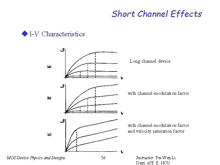
Short Channel Effects u I-V Characteristics Long channel device with channel-modulation factor and velocity saturation factor MOS Device Physics and Designs 56 Instructor: Pei-Wen Li Dept. of E. E. NCU

Short Channel Effects u Vt variation with gate length u Mobility MOS Device Physics and Designs 57 Instructor: Pei-Wen Li Dept. of E. E. NCU

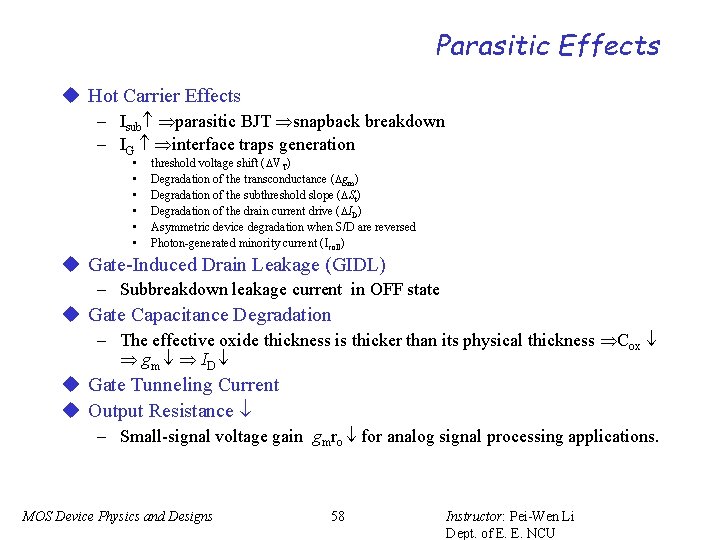
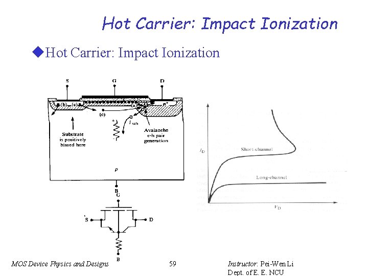
Parasitic Effects u Hot Carrier Effects – Isub parasitic BJT snapback breakdown – IG interface traps generation • • • threshold voltage shift ( VT) Degradation of the transconductance ( gm) Degradation of the subthreshold slope ( St) Degradation of the drain current drive ( ID) Asymmetric device degradation when S/D are reversed Photon-generated minority current (Icoll) u Gate-Induced Drain Leakage (GIDL) – Subbreakdown leakage current in OFF state u Gate Capacitance Degradation – The effective oxide thickness is thicker than its physical thickness Cox gm ID u Gate Tunneling Current u Output Resistance – Small-signal voltage gain gmro for analog signal processing applications. MOS Device Physics and Designs 58 Instructor: Pei-Wen Li Dept. of E. E. NCU

Hot Carrier: Impact Ionization u. Hot Carrier: Impact Ionization MOS Device Physics and Designs 59 Instructor: Pei-Wen Li Dept. of E. E. NCU

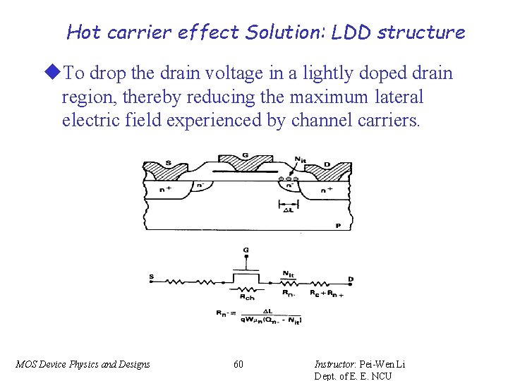
Hot carrier effect Solution: LDD structure u. To drop the drain voltage in a lightly doped drain region, thereby reducing the maximum lateral electric field experienced by channel carriers. MOS Device Physics and Designs 60 Instructor: Pei-Wen Li Dept. of E. E. NCU

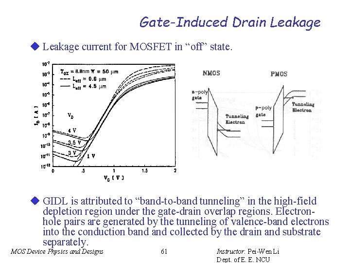
Gate-Induced Drain Leakage u Leakage current for MOSFET in “off” state. u GIDL is attributed to “band-to-band tunneling” in the high-field depletion region under the gate-drain overlap regions. Electronhole pairs are generated by the tunneling of valence-band electrons into the conduction band collected by the drain and substrate separately. MOS Device Physics and Designs 61 Instructor: Pei-Wen Li Dept. of E. E. NCU

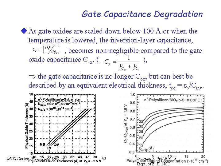
Gate Capacitance Degradation u As gate oxides are scaled down below 100 Å or when the temperature is lowered, the inversion-layer capacitance, , becomes non-negligible compared to the gate oxide capacitance Cox. ( ), the gate capacitance is no longer Cox, but can best be described by an equivalent electrical thickness, teq = o/Cinv. [teq > tox(physical)] MOS Device Physics and Designs 62 Instructor: Pei-Wen Li Dept. of E. E. NCU

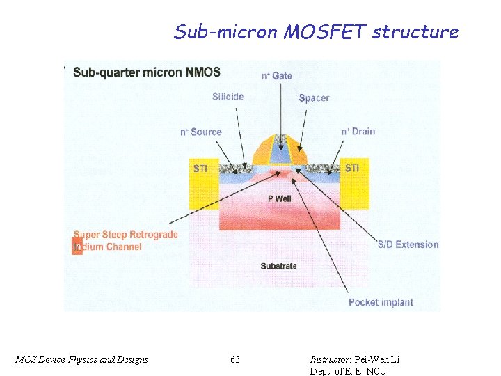
Sub-micron MOSFET structure MOS Device Physics and Designs 63 Instructor: Pei-Wen Li Dept. of E. E. NCU

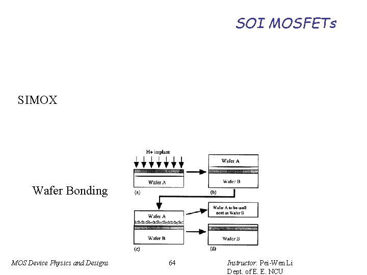
SOI MOSFETs SIMOX Wafer Bonding MOS Device Physics and Designs 64 Instructor: Pei-Wen Li Dept. of E. E. NCU

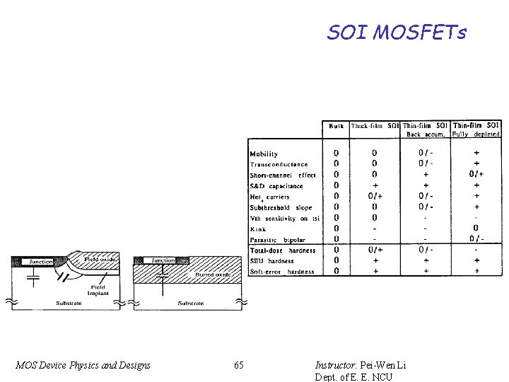
SOI MOSFETs MOS Device Physics and Designs 65 Instructor: Pei-Wen Li Dept. of E. E. NCU

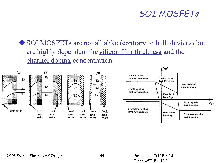
SOI MOSFETs u SOI MOSFETs are not all alike (contrary to bulk devices) but are highly dependent the silicon film thickness and the channel doping concentration. MOS Device Physics and Designs 66 Instructor: Pei-Wen Li Dept. of E. E. NCU

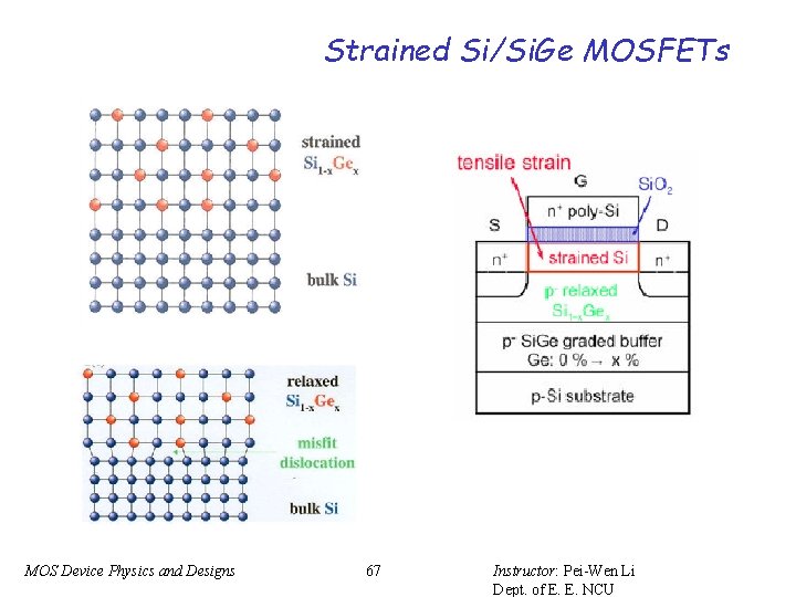
Strained Si/Si. Ge MOSFETs MOS Device Physics and Designs 67 Instructor: Pei-Wen Li Dept. of E. E. NCU

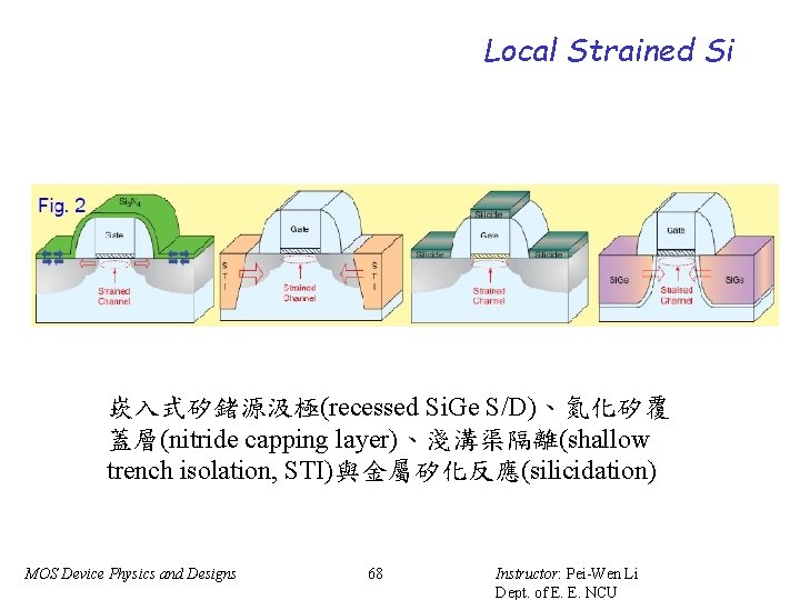
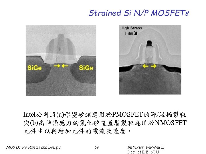
Local Strained Si 崁入式矽鍺源汲極(recessed Si. Ge S/D)、氮化矽覆 蓋層(nitride capping layer)、淺溝渠隔離(shallow trench isolation, STI)與金屬矽化反應(silicidation) MOS Device Physics and Designs 68 Instructor: Pei-Wen Li Dept. of E. E. NCU

Strained Si N/P MOSFETs Intel公司將(a)形變矽鍺應用於PMOSFET的源/汲極製程 與(b)高伸張應力的氮化矽覆蓋層製程應用於NMOSFET 元件中以與增加元件的電流及速度。 MOS Device Physics and Designs 69 Instructor: Pei-Wen Li Dept. of E. E. NCU