Fundamentals of Integrated Circuit Fabrication Objectives This Presentation

Fundamentals of Integrated Circuit Fabrication

Objectives This Presentation deals with the fundamentals of integrated circuit fabrication. In the field of nanotechnology, this basic idea of fabrication is very important from the point of view of semiconductor device engineering. Semi- conductor device fabrication is the process used to create chips for devices that are a part of our everyday use. It is a multiple-step sequence of photographic and chemical processing during which electronic circuits are gradually created on a wafer substrate made of pure semi-conducting material.
The topics include : 1) electronic fundamentals, 2) crystal growth 3) wafer types, 4) transistor types, 5) basic design concepts, 6) mask making, 7) wafer processing, 8) materials used for fabricating the wafer, 9) equipment's used for processing the wafer, 10) clean room standards, 11) testing and reliability control, 12) assembly 13) packaging, and different IC types.
Basics: In the world of semiconductor devices and integrated circuits, silicon is the commonly used semiconductor material, and it is mostly used as a substrate material. For example, solar cells made of silicon wafers are cheaper and can be used for practical applications by common people. Of late, it has been observed that Ga. As fabrication has advanced compared to silicon due to its greater thermal stability, direct band gap and higher electron mobility. However, Ga. As fabrication is a difficult process and the cost is also very high. Today compound semiconductors are the main point of attraction. IV–IV, III–V and II–VI are the common compound semiconductors used in research and industry. Among these the compound semiconductor III–V is widely used as it has multiple applications in LED, LASER, etc. gallium arsenide (Ga. As), indium phosphide (In. P), gallium phosphide (Ga. P) and gallium nitride (Ga. N) and aluminum nitride (Al. N)—are the III–V compound which are widely used. Optoelectronic devices using III–V compound.
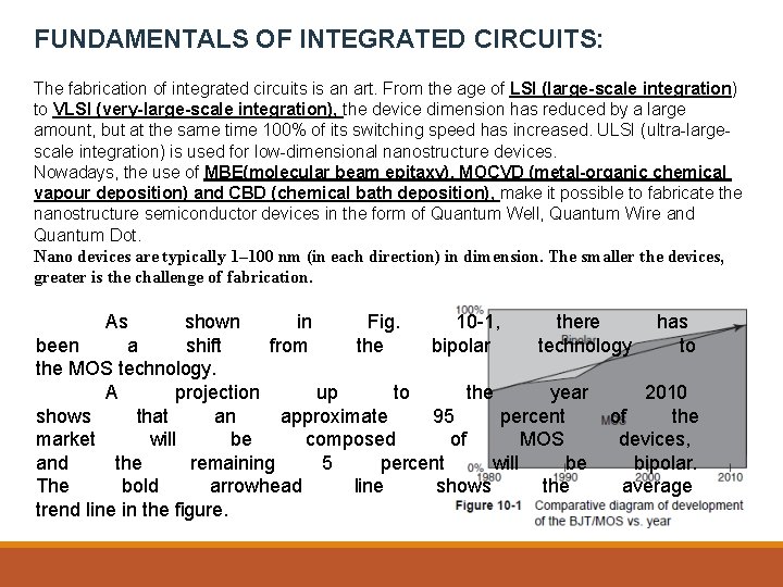
FUNDAMENTALS OF INTEGRATED CIRCUITS: The fabrication of integrated circuits is an art. From the age of LSI (large-scale integration) to VLSI (very-large-scale integration), the device dimension has reduced by a large amount, but at the same time 100% of its switching speed has increased. ULSI (ultra-largescale integration) is used for low-dimensional nanostructure devices. Nowadays, the use of MBE(molecular beam epitaxy), MOCVD (metal-organic chemical vapour deposition) and CBD (chemical bath deposition), make it possible to fabricate the nanostructure semiconductor devices in the form of Quantum Well, Quantum Wire and Quantum Dot. Nano devices are typically 1– 100 nm (in each direction) in dimension. The smaller the devices, greater is the challenge of fabrication. As shown in Fig. 10 -1, there has been a shift from the bipolar technology to the MOS technology. A projection up to the year 2010 shows that an approximate 95 percent of the market will be composed of MOS devices, and the remaining 5 percent will be bipolar. The bold arrowhead line shows the average trend line in the figure.

FUNDAMENTALS OF INTEGRATED CIRCUITS: With devices getting smaller and smaller, the number of their components/chips has been increasingly getting bigger and bigger with time. A plot in Fig. 10 -2 projected up to year 2010 shows the number of components/chip vs. time (year). The bold arrowhead line shows the average trend line in the figure. Figure 10 -3 shows the drop in feature size projected up to the year 2010. The bold arrowhead line shows the average trend line in the figure.
TYPES OF INTEGRATED CIRCUITS: Monolithic IC: In the Monolithic IC the entire circuit is built into a single piece of semiconductor chip, which consists of active and passive components. The most commonly used integrated circuits, microprocessors, memories, etc. , are all monolithic. Hybrid IC: In Hybrid IC the electronic circuit is generally integrated in the ceramic substrate using various components and then enclosed in the single package. The hybrid IC consists of several monolithic ICs connected by metallic interconnects mounted on a common substrate. Hybrid IC technology bonds various substrates either at the die level or at the wafer level. This technology streamlines the connections between different semiconductor chips by replacing wire bonding. This process achieves an accelerated, streamlined and less costly process. Hybrid IC allows increase in communication bandwidth and facilitates higher system yield.

MERITS AND DEMRITS OF INTEGRATED CIRCUITS: The advantages of integrated circuits are as follows: 1. Small in size due to the reduced device dimension 2. Low weight due to very small size 3. Low power requirement due to lower dimension and lower threshold power requirement 4. Low cost due to large-scale production 5. High reliability due to the absence of a solder joint 6. Facilitates integration of large number of devices 7. Improves the device performance even at high-frequency region The disadvantages of integrated circuits are as follows: 1. IC resistors have a limited range 2. Generally inductors (L) cannot be formed using IC 3. Transformers cannot be formed using IC
SCALE OF INTEGRATION: Historically, the first semiconductor IC chips held one diode/transistor. Advancement of technology enabled us to add more and more transistors. The first to arrive was small-scale integration (SSI), then improvements in technique led to devices with hundreds of logic gates—large-scale integration (LSI) Present day micro- processors have millions of logic gates and transistors. Intel co-founder, Gordon E. Moore, in 1965 published a paper on the future projection of IC technology. Moore’s Law is responsible for ―smaller, cheaper and more efficient IC‖. Gordon Moore’s empirical relationship is cited in a number of forms, but its essential thesis is that the number of transistors that can be manufactured on a single die will double every 18 months.
Manufacture of Electronics Components Manufacture of Printed Circuit Boards (PCB’s) Assembly of components on PCB’s
Manufacture of Electronics Components
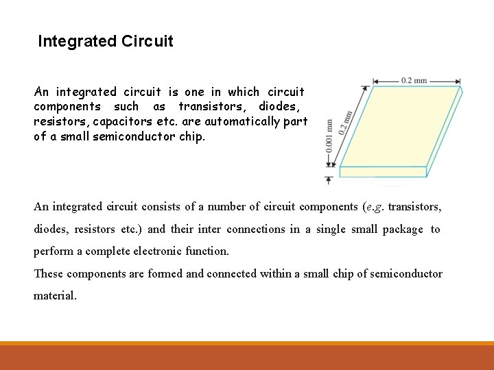
Integrated Circuit An integrated circuit is one in which circuit components such as transistors, diodes, resistors, capacitors etc. are automatically part of a small semiconductor chip. An integrated circuit consists of a number of circuit components (e. g. transistors, diodes, resistors etc. ) and their inter connections in a single small package to perform a complete electronic function. These components are formed and connected within a small chip of semiconductor material.
The following points are worth noting about integrated circuits : (i)In an IC, the various components are automatically part of a small semi-conductor chip and the individual components cannot be removed or replaced. This is in contrast to discrete assembly in which individual components can be removed or replaced if necessary. (ii)The size of an *IC is extremely small. In fact, ICs are so small that you normally need a microscope to see the connections between the components. It is possible to produce circuits containing many transistors, diodes, resistors etc. on the surface of this small chip. (iii)No components of an IC are seen to project above the surface of the chip. This is because all the components are formed within the chip.

Advantages and Disadvantages of Integrated Circuits Integrated circuits possess the following advantages over discrete circuits : i. iii. iv. v. vii. Increased reliability due to lesser number of connections. Extremely small size due to the fabrication of various circuit elements in a single chip of semi-conductor material. Lesser weight and **space requirement due to miniaturized circuit. Low power requirements. Greater ability to operate at extreme values of temperature. Low cost because of simultaneous production of hundreds of alike circuits on a small semiconductor wafer. The circuit lay out is greatly simplified because integrated circuits are constrained to use minimum number of external connections. * Since it combines both active (e. g. , transistors, diodes etc. ) and passive elements (e. g. , resistors, capacitors etc. ) in a monolithic structure, the complete unit is called an integrated circuit. ** Typically, this is about 10% of the space required by comparable discrete assembly.
Disadvantages : The disadvantages of integrated circuits are : i. If any component in an IC goes out of order, the whole IC has to be replaced by the new one. ii. In an IC, it is neither convenient nor economical to fabricate capacitances exceeding 30 p. F. Therefore, for high values of capacitance, discrete components exterior to IC chip are connected. iii. It is not possible to fabricate inductors and transformers on the surface of semi-conductor chip. Therefore, these components are connected exterior to the semi-conductor chip. iv. It is not possible to produce high power ICs (greater than 10 W). v. There is a lack of flexibility in an IC i. e. , it is generally not possible to modify the parameters within which an integrated circuit will operate.
IC Classifications Four basic types of constructions are employed in the manufacture of integrated circuits, namely ; i. mono-lithic ii. thin-film iii. thick-film iv. hybrid. Monolithic ICs are by far the most common type used in practice.
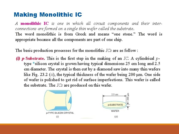
Making Monolithic IC A monolithic IC is one in which all circuit components and their interconnections are formed on a single thin wafer called the substrate. The word monolithic is from Greek and means “one stone. ” The word is appropriate because all the components are part of one chip. The basic production processes for the monolithic ICs are as follow : (i) p-Substrate. This is the first step in the making of an IC. A cylindrical ptype *silicon crystal is grown having typical dimensions 25 cm long and 2. 5 cm diameter. The crystal is then cut by a diamond saw into many thin wafers like Fig. 23. 2 (ii), the typical thickness of the wafer being 200 μm. One side of wafer is polished to get rid of surface imperfections. This wafer is called the substrate. The ICs are produced on this wafer.
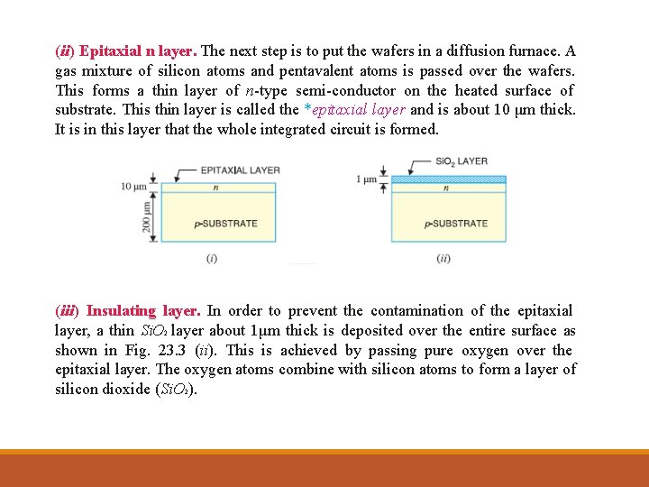
(ii) Epitaxial n layer. The next step is to put the wafers in a diffusion furnace. A gas mixture of silicon atoms and pentavalent atoms is passed over the wafers. This forms a thin layer of n-type semi-conductor on the heated surface of substrate. This thin layer is called the *epitaxial layer and is about 10 μm thick. It is in this layer that the whole integrated circuit is formed. (iii) Insulating layer. In order to prevent the contamination of the epitaxial layer, a thin Si. O 2 layer about 1μm thick is deposited over the entire surface as shown in Fig. 23. 3 (ii). This is achieved by passing pure oxygen over the epitaxial layer. The oxygen atoms combine with silicon atoms to form a layer of silicon dioxide (Si. O 2).
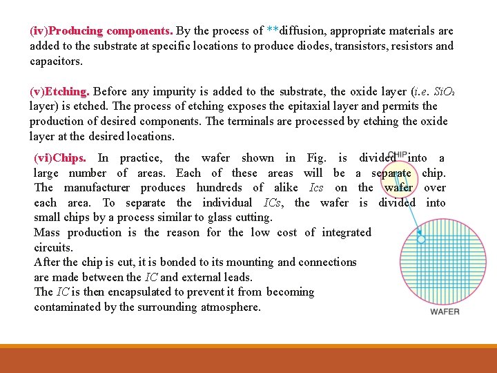
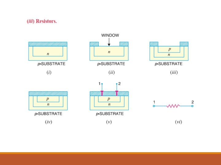
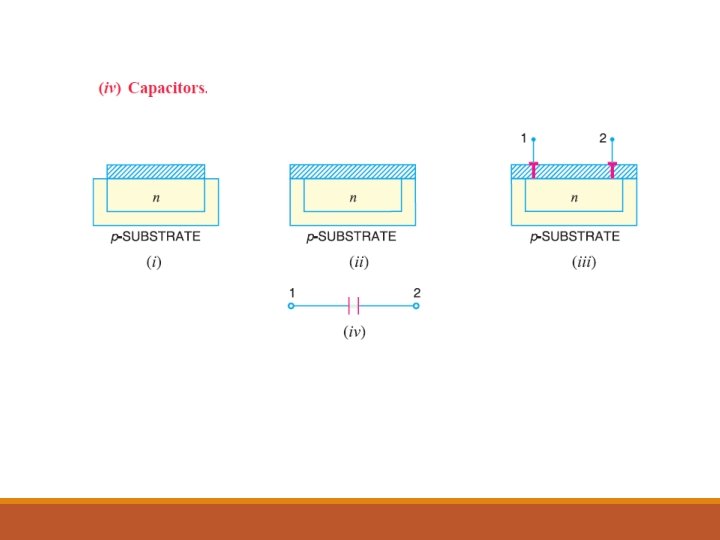
(iv)Producing components. By the process of **diffusion, appropriate materials are added to the substrate at specific locations to produce diodes, transistors, resistors and capacitors. (v)Etching. Before any impurity is added to the substrate, the oxide layer (i. e. Si. O 2 layer) is etched. The process of etching exposes the epitaxial layer and permits the production of desired components. The terminals are processed by etching the oxide layer at the desired locations. (vi)Chips. In practice, the wafer shown in Fig. is divided into a large number of areas. Each of these areas will be a separate chip. The manufacturer produces hundreds of alike Ics on the wafer over each area. To separate the individual ICs, the wafer is divided into small chips by a process similar to glass cutting. Mass production is the reason for the low cost of integrated circuits. After the chip is cut, it is bonded to its mounting and connections are made between the IC and external leads. The IC is then encapsulated to prevent it from becoming contaminated by the surrounding atmosphere.
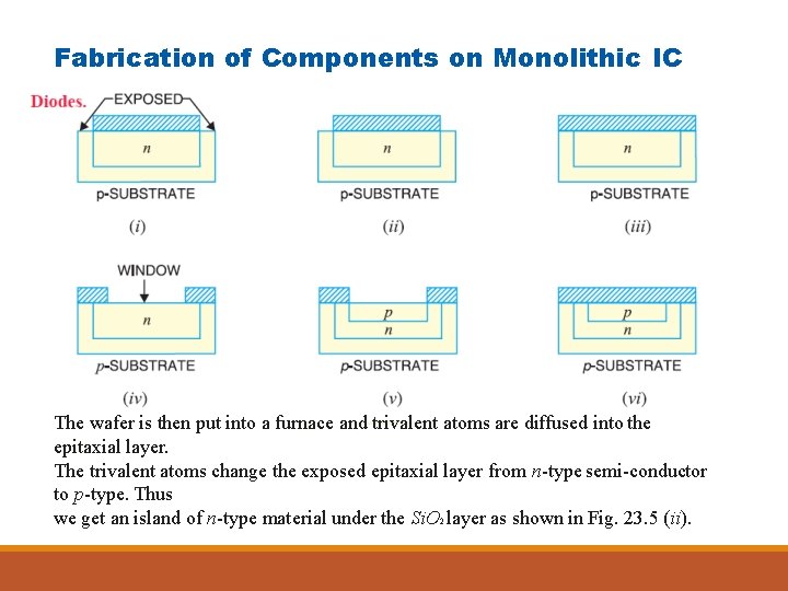
Fabrication of Components on Monolithic IC The wafer is then put into a furnace and trivalent atoms are diffused into the epitaxial layer. The trivalent atoms change the exposed epitaxial layer from n-type semi-conductor to p-type. Thus we get an island of n-type material under the Si. O 2 layer as shown in Fig. 23. 5 (ii).
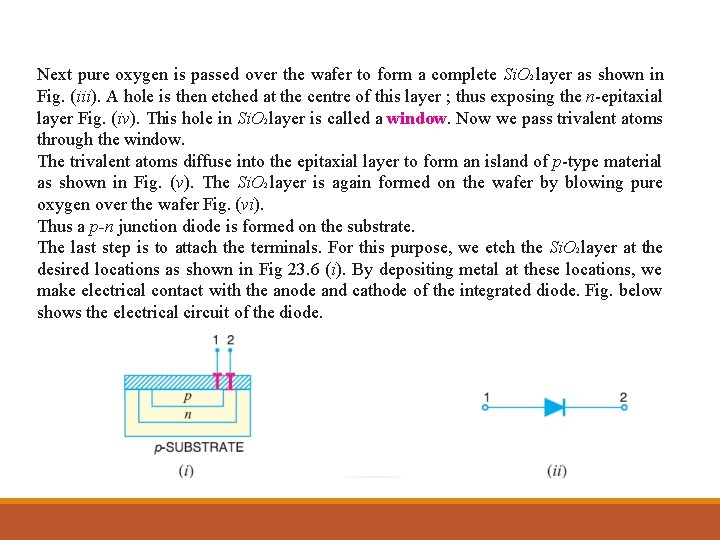
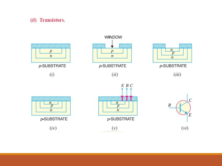
Next pure oxygen is passed over the wafer to form a complete Si. O 2 layer as shown in Fig. (iii). A hole is then etched at the centre of this layer ; thus exposing the n-epitaxial layer Fig. (iv). This hole in Si. O 2 layer is called a window. Now we pass trivalent atoms through the window. The trivalent atoms diffuse into the epitaxial layer to form an island of p-type material as shown in Fig. (v). The Si. O 2 layer is again formed on the wafer by blowing pure oxygen over the wafer Fig. (vi). Thus a p-n junction diode is formed on the substrate. The last step is to attach the terminals. For this purpose, we etch the Si. O 2 layer at the desired locations as shown in Fig 23. 6 (i). By depositing metal at these locations, we make electrical contact with the anode and cathode of the integrated diode. Fig. below shows the electrical circuit of the diode.
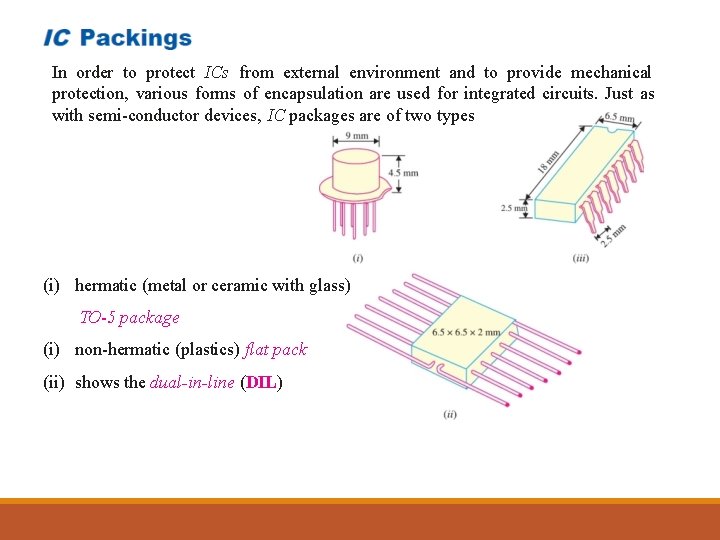
In order to protect ICs from external environment and to provide mechanical protection, various forms of encapsulation are used for integrated circuits. Just as with semi-conductor devices, IC packages are of two types (i) hermatic (metal or ceramic with glass) TO-5 package (i) non-hermatic (plastics) flat pack (ii) shows the dual-in-line (DIL)
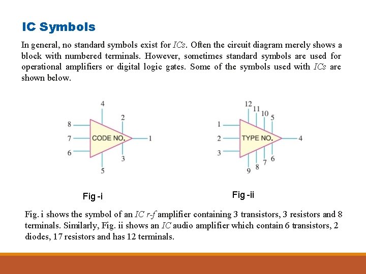
IC Symbols In general, no standard symbols exist for ICs. Often the circuit diagram merely shows a block with numbered terminals. However, sometimes standard symbols are used for operational amplifiers or digital logic gates. Some of the symbols used with ICs are shown below. Fig -ii Fig. i shows the symbol of an IC r-f amplifier containing 3 transistors, 3 resistors and 8 terminals. Similarly, Fig. ii shows an IC audio amplifier which contain 6 transistors, 2 diodes, 17 resistors and has 12 terminals.

POINTS TO REMEMBER: 1. In monolithic circuits, the entire circuit is built into a single piece of semiconductor chip consisting of passive and active components; physical properties of the semiconductor determine performance of the circuit. 2. Hybrid integrated circuits are devices that apply standard semiconductor processing technology to individual ICs, and fuse them together to simultaneously form an electrical, mechanical, and thermal bond. 3. Hybrid integrated circuit offers a new a paradigm in integrated circuit and system designs and architectures by permitting: (a) Increase in communication bandwidth (b) Modular chip design process (c) Higher system yields with more reliability 4. Integrated circuits have the following advantages: (a) Small in size due to the reduced device dimension (b) Low weight due to very small size (c) Low power requirement due to lower dimension and lower threshold power requirement (d) Low cost due to large-scale production 5. The Czochralski process is used to grow ingot and subsequently to design the wafer.
POINTS TO REMEMBER: 6. The epitaxial process is used to form a layer of single-crystal silicon on an existing crystal wafer of the same or different material. 7. Thermal oxidation of silicon is achieved in the presence of water vapour; this process is called wet oxidation. 8. The process for pattern definition by applying thin uniform layer of viscous liquid photo resist on the wafer surface is the photolithography process. 9. The composite drawing of the circuit is partitioned into several levels called masking levels, used in fabricating the chip. 10. Etching is the process of removing the unwanted portion of the layer or region from the surface during the fabrication process. Etching can be of two types: (a) Dry etching (b) Chemical etching 11. Diffusion of impurities into substrate layer is the basic step in the planar process. 12. The ionized particles are accelerated through an electrical field and targeted at the semiconductor Wafer. 13. The metallization process is used to form the interconnections of the components on the chip. 14. IC testing is performed before packaging.
- Slides: 29