Fully Depleted Low Power CMOS Detectors Konstantin Stefanov
- Slides: 15

Fully Depleted Low Power CMOS Detectors Konstantin Stefanov 8 June 2015

Back side biased CMOS image sensor development • We have a project to design back-side biased, thick sensitive area CMOS image sensors achieving full depletion – Funded by the UK Space Agency – 1 year project • Demand for thick (>100 µm), fully depleted CMOS sensors with high QE: – Near-IR for astronomy, Earth observation, hyperspectral imaging, high speed imaging, spectroscopy, microscopy and surveillance. – Soft X-ray (up to 10 ke. V) imaging at synchrotron light sources and free electron lasers requires substrate thickness >200 µm • Low noise and high CVF are essential to most applications – pinned photodiode is required 2 Konstantin Stefanov, 8 June 2015

Back side biased CMOS image sensor development • Present experience with CMOS: – ESPROS: bulk 10 kΩ. cm, 50 µm thick filly depleted • We have designed a chip already • CCD sense element with rather high dark current • ESPROS has no plans to increase thickness in the near future – Tower. Jazz: 1 kΩ. cm epi, thickness up to 18 µm • Good pinned photodiode available • Epi thickness can be increased in principle to 100 µm – new (untested) advances in epi manufacture • Our goal is to design back-side biased CMOS demonstrator – Initially on easily available substrates (e. g. 18 µm), with or without thinning – Demonstrate successful operation – Eventually move on to thicker substrates 3 Konstantin Stefanov, 8 June 2015

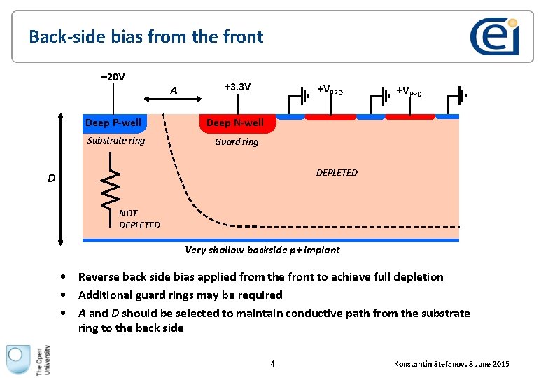
Back-side bias from the front – 20 V Deep P-well Substrate ring A +3. 3 V +VPPD Deep N-well Guard ring DEPLETED D NOT DEPLETED Very shallow backside p+ implant • Reverse back side bias applied from the front to achieve full depletion • Additional guard rings may be required • A and D should be selected to maintain conductive path from the substrate ring to the back side 4 Konstantin Stefanov, 8 June 2015

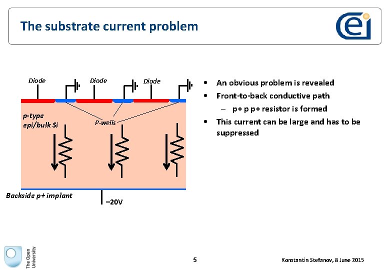
The substrate current problem Diode p-type epi/bulk Si Backside p+ implant Diode • An obvious problem is revealed • Front-to-back conductive path – p+ p p+ resistor is formed • This current can be large and has to be suppressed P-wells – 20 V 5 Konstantin Stefanov, 8 June 2015

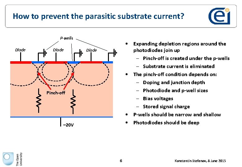
How to prevent the parasitic substrate current? P-wells Diode • Expanding depletion regions around the photodiodes join up – Pinch-off is created under the p-wells – Substrate current is eliminated • The pinch-off condition depends on: – Doping and junction depth – Photodiode and p-well sizes – Bias voltages – Stored signal charge • P-wells should be narrow and shallow • Photodiodes should be deep Diode Pinch-off – 20 V 6 Konstantin Stefanov, 8 June 2015

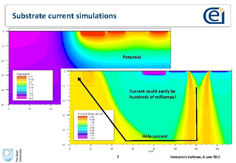
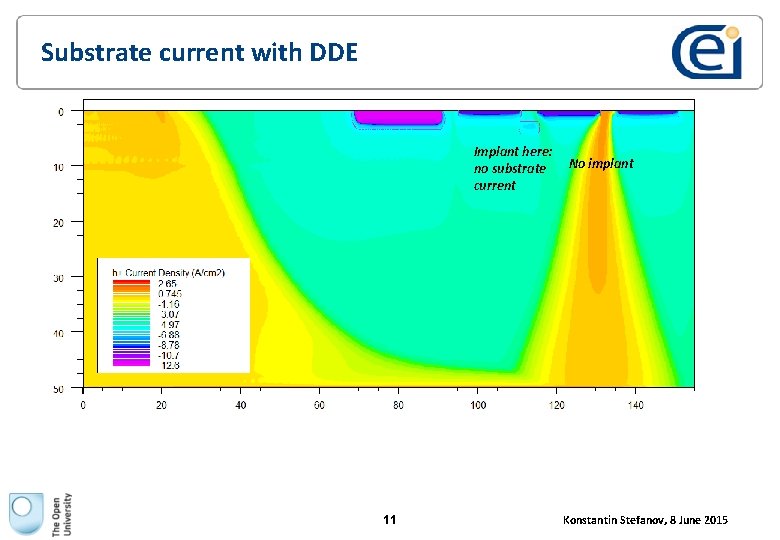
Substrate current simulations Potential Current could easily be hundreds of milliamps! Hole current 7 Konstantin Stefanov, 8 June 2015

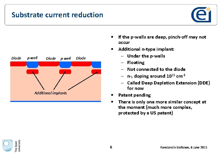
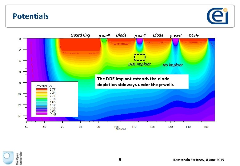
Substrate current reduction Diode p-well Additional implants Diode • If the p-wells are deep, pinch-off may not occur • Additional n-type implant: – Under the p-wells – Floating – Not connected to the diode – n-, doping around 1015 cm-3 – Called Deep Depletion Extension (DDE) for now • Patent pending • There is only one more similar concept at the moment (much more complex, protected by a US patent) 8 Konstantin Stefanov, 8 June 2015

Potentials Guard ring p-well Diode p-well DDE Implant Diode p-well Diode No implant The DDE implant extends the diode depletion sideways under the p-wells 9 Konstantin Stefanov, 8 June 2015

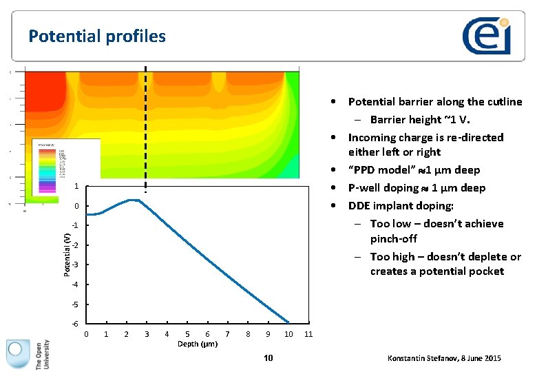
Potential profiles • Potential barrier along the cutline – Barrier height ~1 V. • Incoming charge is re-directed either left or right • “PPD model” 1 µm deep • P-well doping 1 µm deep • DDE implant doping: – Too low – doesn’t achieve pinch-off – Too high – doesn’t deplete or creates a potential pocket 1 0 Potential (V) -1 -2 -3 -4 -5 -6 0 1 2 3 4 5 6 Depth (μm) 7 8 9 10 10 11 Konstantin Stefanov, 8 June 2015

Substrate current with DDE Implant here: no substrate current 11 No implant Konstantin Stefanov, 8 June 2015

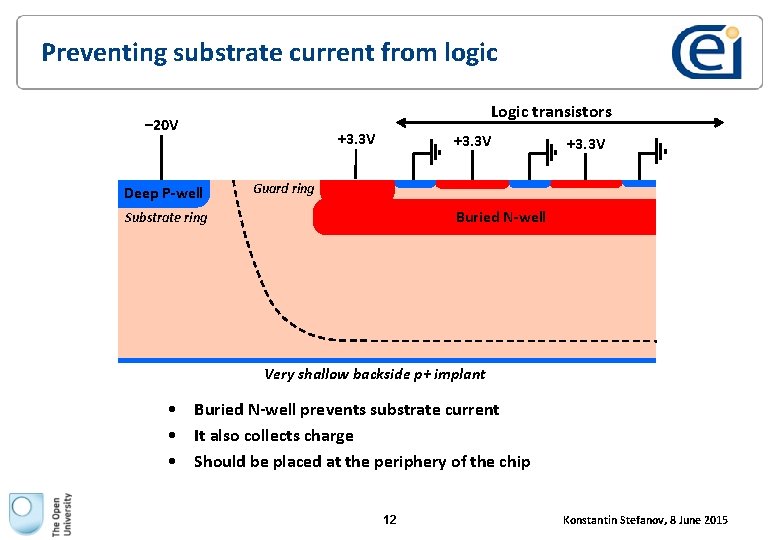
Preventing substrate current from logic Logic transistors – 20 V Deep P-well +3. 3 V Guard ring Buried N-well Substrate ring Very shallow backside p+ implant • Buried N-well prevents substrate current • It also collects charge • Should be placed at the periphery of the chip 12 Konstantin Stefanov, 8 June 2015

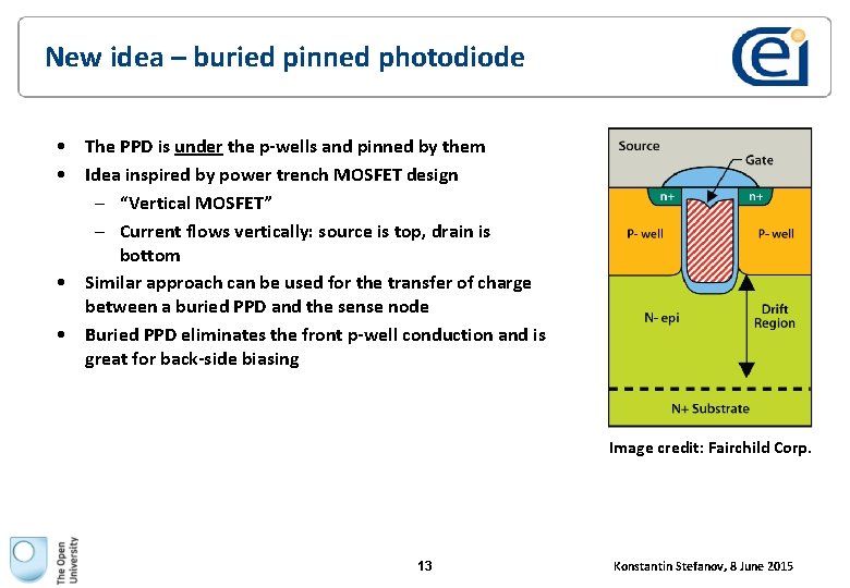
New idea – buried pinned photodiode • The PPD is under the p-wells and pinned by them • Idea inspired by power trench MOSFET design – “Vertical MOSFET” – Current flows vertically: source is top, drain is bottom • Similar approach can be used for the transfer of charge between a buried PPD and the sense node • Buried PPD eliminates the front p-well conduction and is great for back-side biasing Image credit: Fairchild Corp. 13 Konstantin Stefanov, 8 June 2015

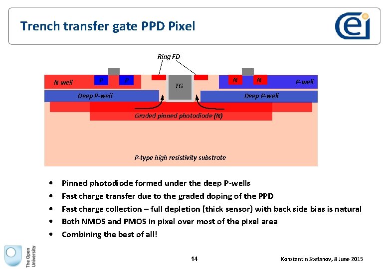
Trench transfer gate PPD Pixel Ring FD N-well P P TG TG N Deep P-well N P-well Deep P-well Graded pinned photodiode (N) P-type high resistivity substrate • • • Pinned photodiode formed under the deep P-wells Fast charge transfer due to the graded doping of the PPD Fast charge collection – full depletion (thick sensor) with back side bias is natural Both NMOS and PMOS in pixel over most of the pixel area Combining the best of all! 14 Konstantin Stefanov, 8 June 2015

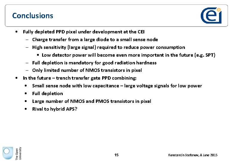
Conclusions • Fully depleted PPD pixel under development at the CEI – Charge transfer from a large diode to a small sense node – High sensitivity (large signal) required to reduce power consumption • Low detector power will become even more important in the future (e. g. SPT) – Full depletion is mandatory for good radiation hardness – Only limited number of NMOS transistors in pixel • In the future – trench transfer gate PPD combining: • Small sense node with low capacitance – large voltage signals for low power • Full depletion • Large number of NMOS and PMOS transistors in pixel • Rival to hybrid APS? 15 Konstantin Stefanov, 8 June 2015