Fully depleted CMOS sensor using reverse substrate bias
Fully depleted CMOS sensor using reverse substrate bias Konstantin Stefanov 4 May 2017
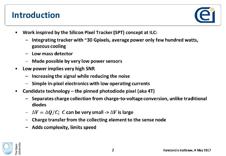
Introduction • 2 Konstantin Stefanov, 4 May 2017
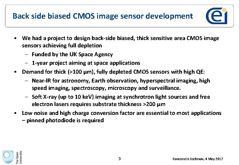
Back side biased CMOS image sensor development • We had a project to design back-side biased, thick sensitive area CMOS image sensors achieving full depletion – Funded by the UK Space Agency – 1 -year project aiming at space applications • Demand for thick (>100 µm), fully depleted CMOS sensors with high QE: – Near-IR for astronomy, Earth observation, hyperspectral imaging, high speed imaging, spectroscopy, microscopy and surveillance. – Soft X-ray (up to 10 ke. V) imaging at synchrotron light sources and free electron lasers requires substrate thickness >200 µm • Low noise and high charge conversion factor are essential to most applications – pinned photodiode is required 3 Konstantin Stefanov, 4 May 2017
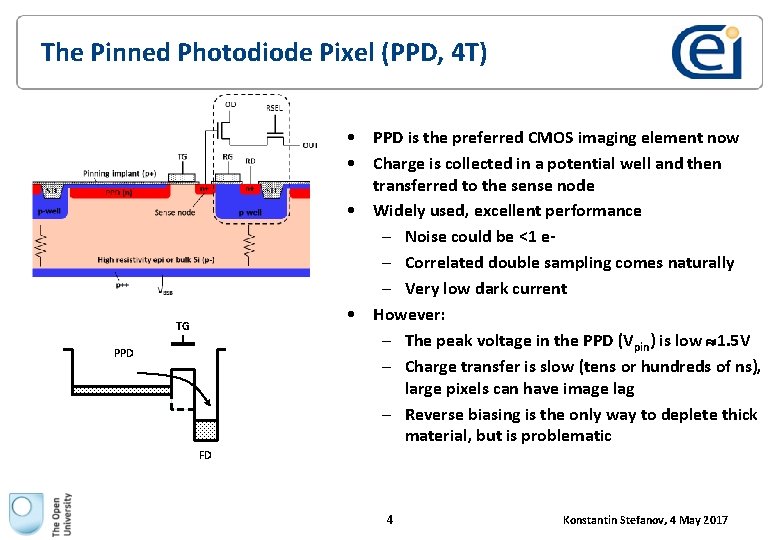
The Pinned Photodiode Pixel (PPD, 4 T) • PPD is the preferred CMOS imaging element now • Charge is collected in a potential well and then transferred to the sense node • Widely used, excellent performance – Noise could be <1 e– Correlated double sampling comes naturally – Very low dark current • However: – The peak voltage in the PPD (Vpin) is low 1. 5 V – Charge transfer is slow (tens or hundreds of ns), large pixels can have image lag – Reverse biasing is the only way to deplete thick material, but is problematic TG PPD FD 4 Konstantin Stefanov, 4 May 2017
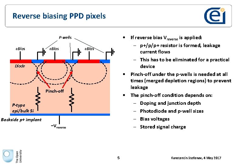
Reverse biasing PPD pixels • If reverse bias Vreverse is applied: – p+/p/p+ resistor is formed, leakage current flows – This has to be eliminated for a practical device • Pinch-off under the p-wells is needed at all times (merged depletion regions) to prevent leakage • The pinch-off condition depends on: – Doping and junction depth – Photodiode and p-well sizes – Bias voltages – Stored signal charge P-wells +Bias Diode Pinch-off P-type epi/bulk Si Backside p+ implant –Vreverse 5 Konstantin Stefanov, 4 May 2017
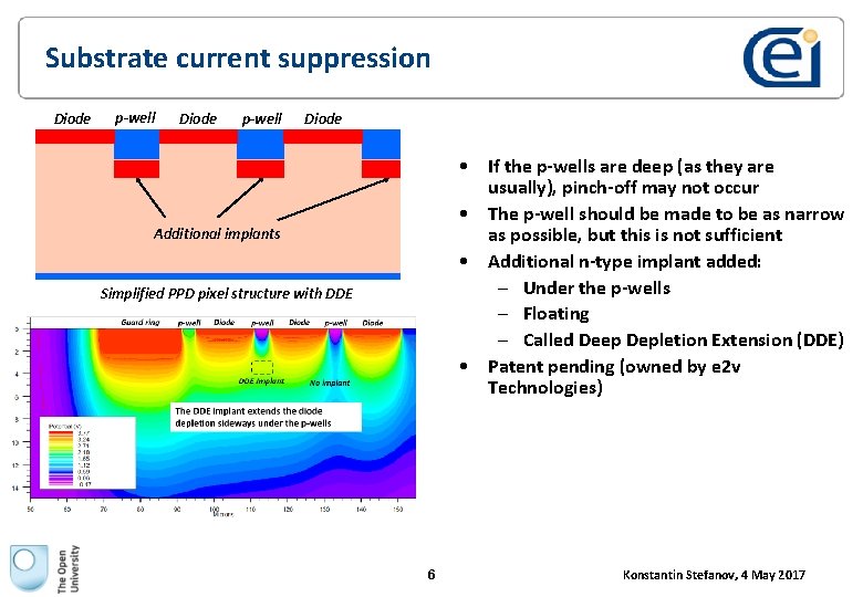
Substrate current suppression Diode p-well Diode • If the p-wells are deep (as they are usually), pinch-off may not occur • The p-well should be made to be as narrow as possible, but this is not sufficient • Additional n-type implant added: – Under the p-wells – Floating – Called Deep Depletion Extension (DDE) • Patent pending (owned by e 2 v Technologies) Additional implants Simplified PPD pixel structure with DDE 6 Konstantin Stefanov, 4 May 2017
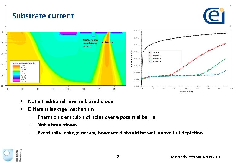
Substrate current • Not a traditional reverse biased diode • Different leakage mechanism – Thermionic emission of holes over a potential barrier – Not a breakdown – Eventually leakage occurs, however it should be well above full depletion 7 Konstantin Stefanov, 4 May 2017
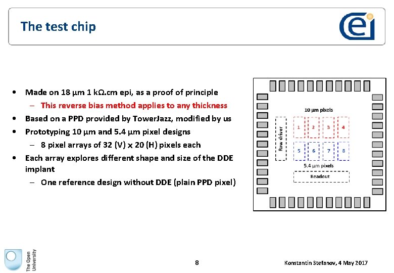
The test chip • Made on 18 µm 1 kΩ. cm epi, as a proof of principle – This reverse bias method applies to any thickness • Based on a PPD provided by Tower. Jazz, modified by us • Prototyping 10 µm and 5. 4 µm pixel designs – 8 pixel arrays of 32 (V) 20 (H) pixels each • Each array explores different shape and size of the DDE implant – One reference design without DDE (plain PPD pixel) 8 Konstantin Stefanov, 4 May 2017
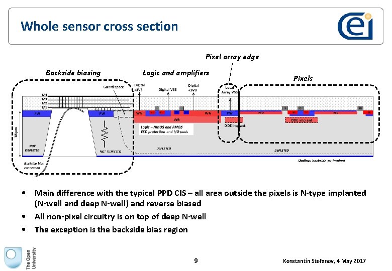
Whole sensor cross section Pixel array edge Backside biasing Logic and amplifiers Pixels • Main difference with the typical PPD CIS – all area outside the pixels is N-type implanted (N-well and deep N-well) and reverse biased • All non-pixel circuitry is on top of deep N-well • The exception is the backside bias region 9 Konstantin Stefanov, 4 May 2017
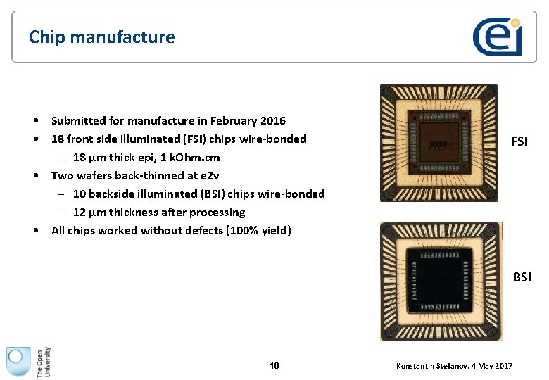
Chip manufacture • Submitted for manufacture in February 2016 • 18 front side illuminated (FSI) chips wire-bonded – 18 µm thick epi, 1 k. Ohm. cm • Two wafers back-thinned at e 2 v – 10 backside illuminated (BSI) chips wire-bonded – 12 µm thickness after processing • All chips worked without defects (100% yield) FSI BSI 10 Konstantin Stefanov, 4 May 2017
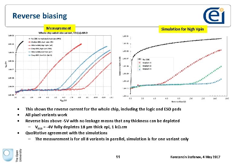
Reverse biasing Measurement • • Simulation for high Vpin This shows the reverse current for the whole chip, including the logic and ESD pads All pixel variants work Reverse bias above -5 V with no leakage means that any thickness can be depleted – VBSB = -4 V fully depletes 18 µm thick epi, 1 kΩ. cm Qualitative agreement with the simulations – The measurement is for all 8 variants in parallel, simulation is for one variant only 11 Konstantin Stefanov, 4 May 2017
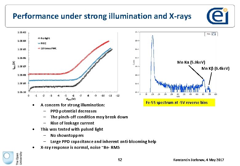
Performance under strong illumination and X-rays Mn Kα (5. 9 ke. V) Mn Kβ (6. 4 ke. V) • • • Fe-55 spectrum at -5 V reverse bias A concern for strong illumination: – PPD potential decreases – The pinch-off condition may break down – Rise of leakage current This was tested with pulsed light – No showstoppers – Large PPD capacitance and inherent anti-blooming help X-ray response is normal, noise ~8 e- RMS 12 Konstantin Stefanov, 4 May 2017
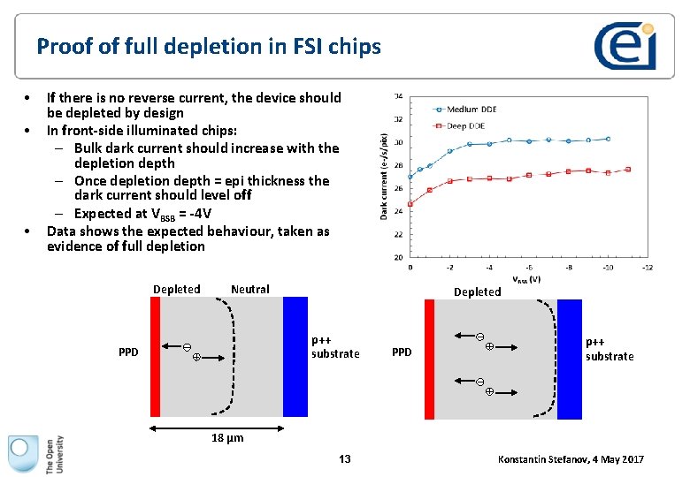
Proof of full depletion in FSI chips • • • If there is no reverse current, the device should be depleted by design In front-side illuminated chips: – Bulk dark current should increase with the depletion depth – Once depletion depth = epi thickness the dark current should level off – Expected at VBSB = -4 V Data shows the expected behaviour, taken as evidence of full depletion Depleted Neutral Depleted p++ substrate PPD p++ substrate 18 µm 13 Konstantin Stefanov, 4 May 2017
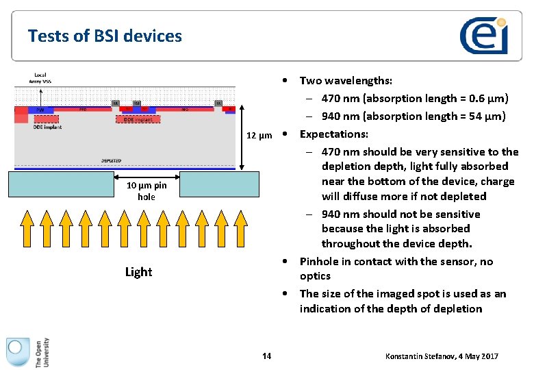
Tests of BSI devices 12 µm 10 µm pin hole Light 14 • Two wavelengths: – 470 nm (absorption length = 0. 6 µm) – 940 nm (absorption length = 54 µm) • Expectations: – 470 nm should be very sensitive to the depletion depth, light fully absorbed near the bottom of the device, charge will diffuse more if not depleted – 940 nm should not be sensitive because the light is absorbed throughout the device depth. • Pinhole in contact with the sensor, no optics • The size of the imaged spot is used as an indication of the depth of depletion Konstantin Stefanov, 4 May 2017
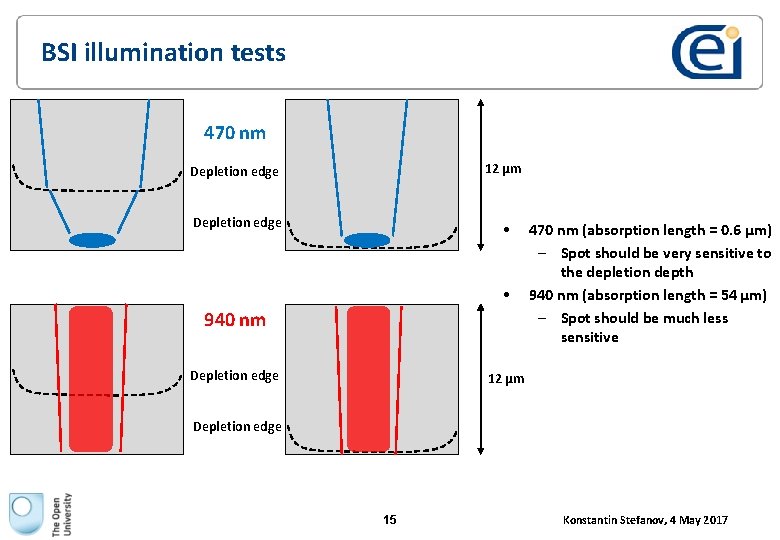
BSI illumination tests 470 nm Depletion edge 12 µm Depletion edge • • 940 nm Depletion edge 470 nm (absorption length = 0. 6 µm) – Spot should be very sensitive to the depletion depth 940 nm (absorption length = 54 µm) – Spot should be much less sensitive 12 µm Depletion edge 15 Konstantin Stefanov, 4 May 2017
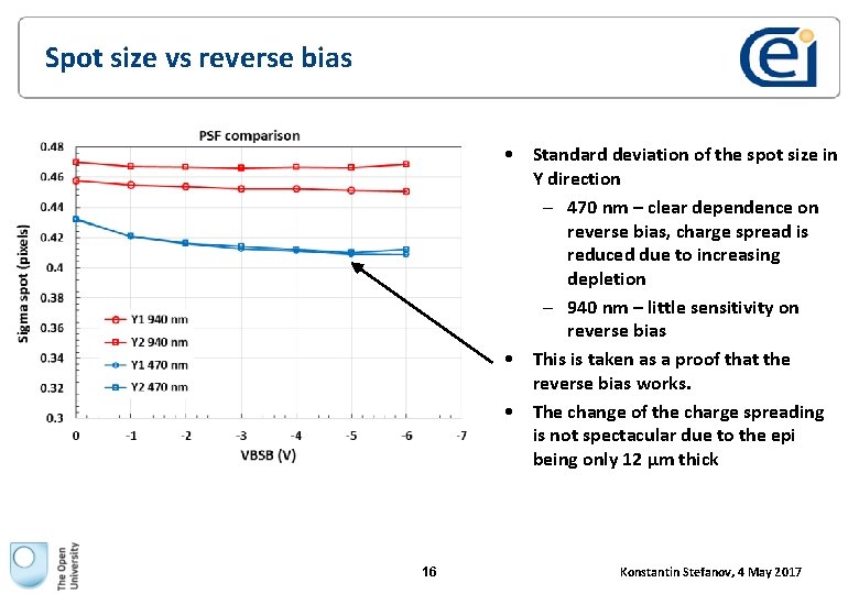
Spot size vs reverse bias • Standard deviation of the spot size in Y direction – 470 nm – clear dependence on reverse bias, charge spread is reduced due to increasing depletion – 940 nm – little sensitivity on reverse bias • This is taken as a proof that the reverse bias works. • The change of the charge spreading is not spectacular due to the epi being only 12 µm thick 16 Konstantin Stefanov, 4 May 2017
Summary • New fully depleted monolithic PPD CMOS sensor using reverse substrate bias demonstrated – First prototype designed on 18 µm, 1 kΩ. cm epi as a proof of principle – Can be scaled to much thicker epi/bulk substrates – Both FSI and BSI devices manufactured, full depletion proven • Advantages for HEP: – Fully depleted, radiation hard, few electrons noise, large SNR, low power, large pixels can be made • Disadvantages: – Charge transfer to sense node limits speed to few µs/row, very limited electronics per pixel, best suited for integrating detectors 17 Konstantin Stefanov, 4 May 2017
- Slides: 17