Full Custom Associative Memory Core With respect to
- Slides: 19

Full Custom Associative Memory Core With respect to standard cell design of the memory chip we want to: Increase memory density Reduce power consumption

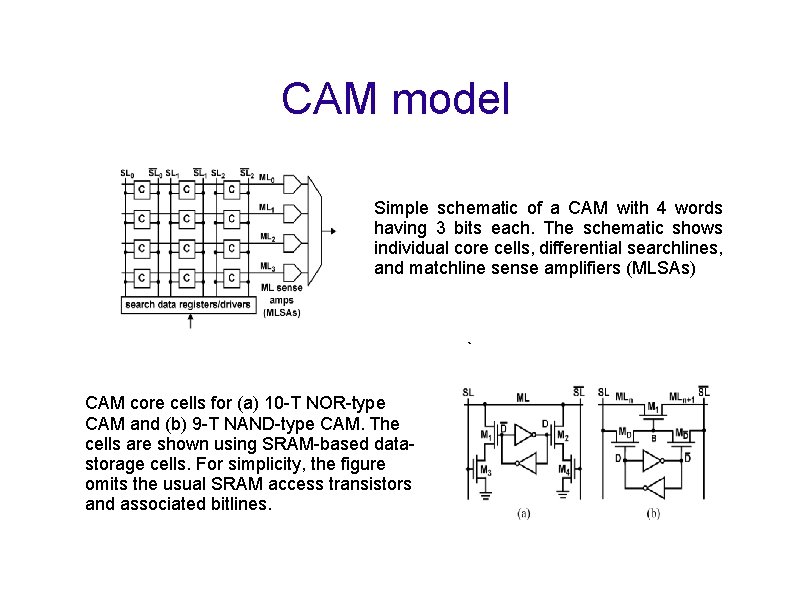
CAM model Simple schematic of a CAM with 4 words having 3 bits each. The schematic shows individual core cells, differential searchlines, and matchline sense amplifiers (MLSAs) ` CAM core cells for (a) 10 -T NOR-type CAM and (b) 9 -T NAND-type CAM. The cells are shown using SRAM-based datastorage cells. For simplicity, the figure omits the usual SRAM access transistors and associated bitlines.

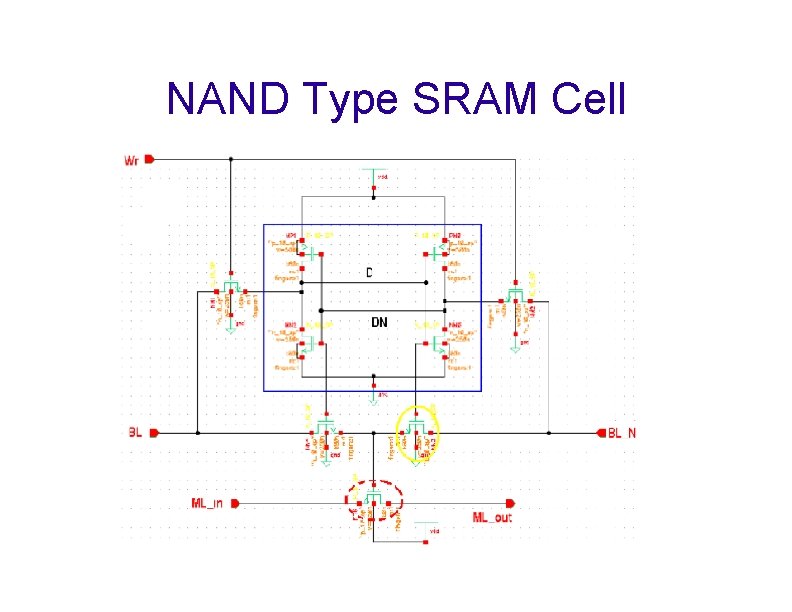
NAND Type SRAM Cell

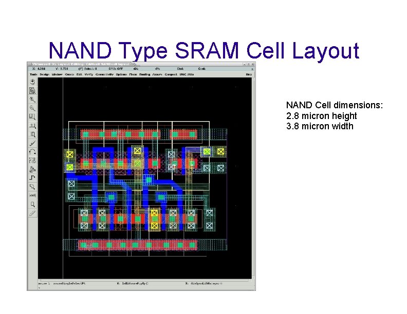
NAND Type SRAM Cell Layout NAND Cell dimensions: 2. 8 micron height 3. 8 micron width

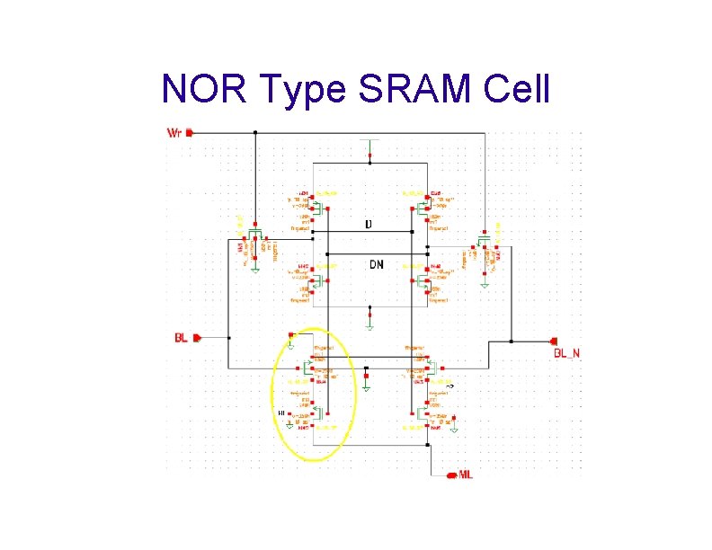
NOR Type SRAM Cell

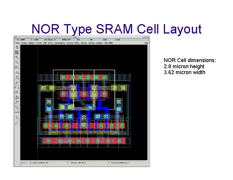
NOR Type SRAM Cell Layout NOR Cell dimensions: 2. 8 micron height 3. 62 micron width

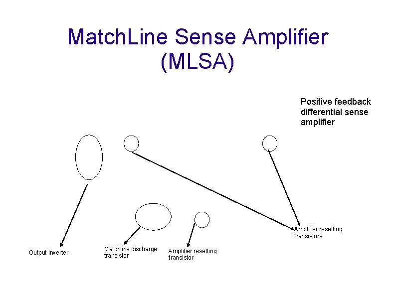
Match. Line Sense Amplifier (MLSA) Positive feedback differential sense amplifier Amplifier resetting transistors Output inverter Matchline discharge transistor Amplifier resetting transistor

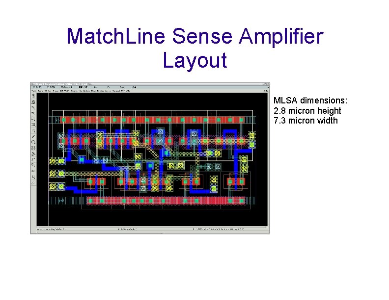
Match. Line Sense Amplifier Layout MLSA dimensions: 2. 8 micron height 7. 3 micron width

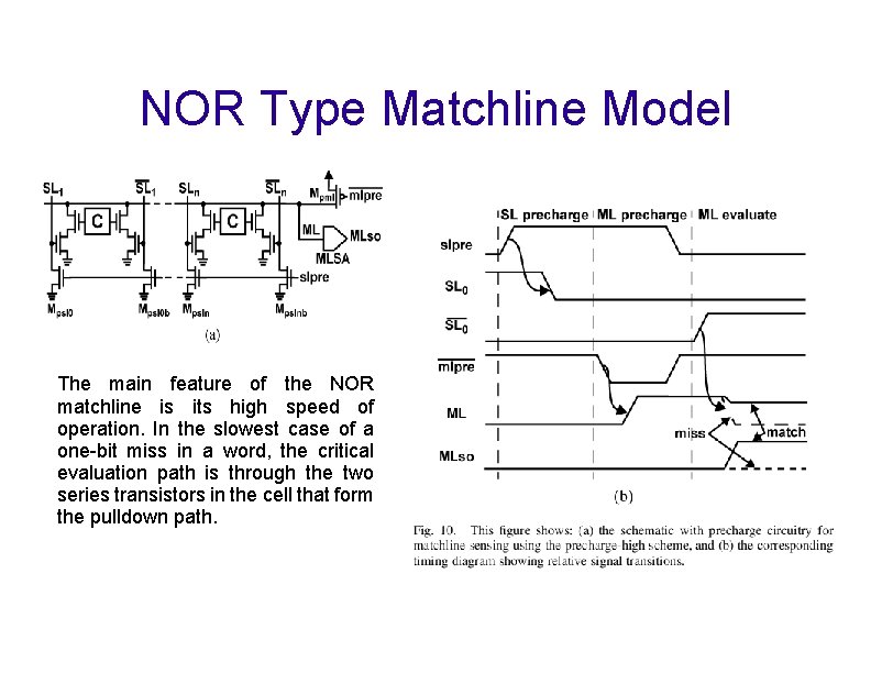
NOR Type Matchline Model The main feature of the NOR matchline is its high speed of operation. In the slowest case of a one-bit miss in a word, the critical evaluation path is through the two series transistors in the cell that form the pulldown path.

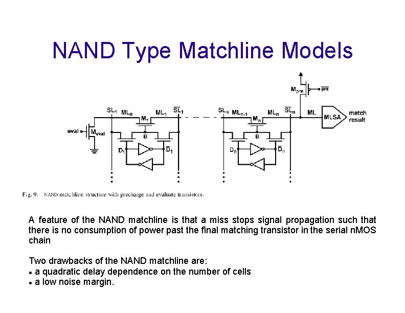
NAND Type Matchline Models A feature of the NAND matchline is that a miss stops signal propagation such that there is no consumption of power past the final matching transistor in the serial n. MOS chain Two drawbacks of the NAND matchline are: a quadratic delay dependence on the number of cells a low noise margin.

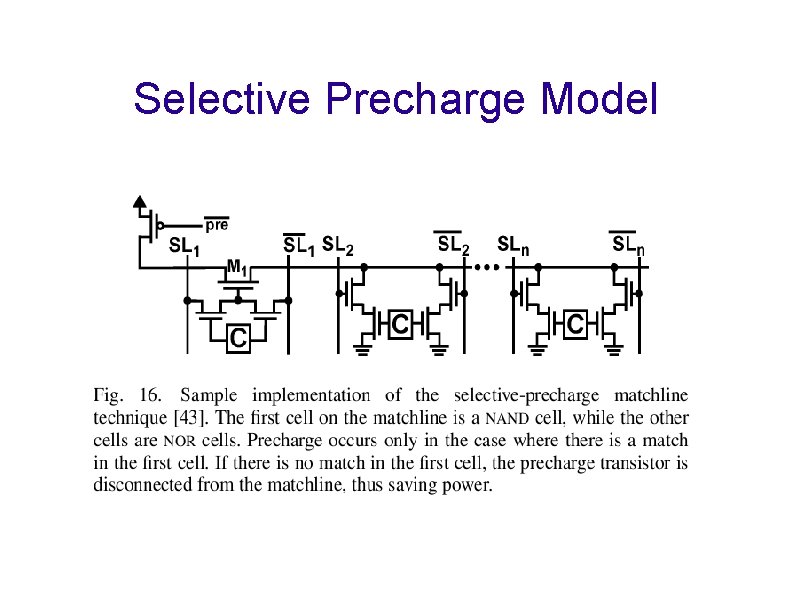
Selective Precharge Model

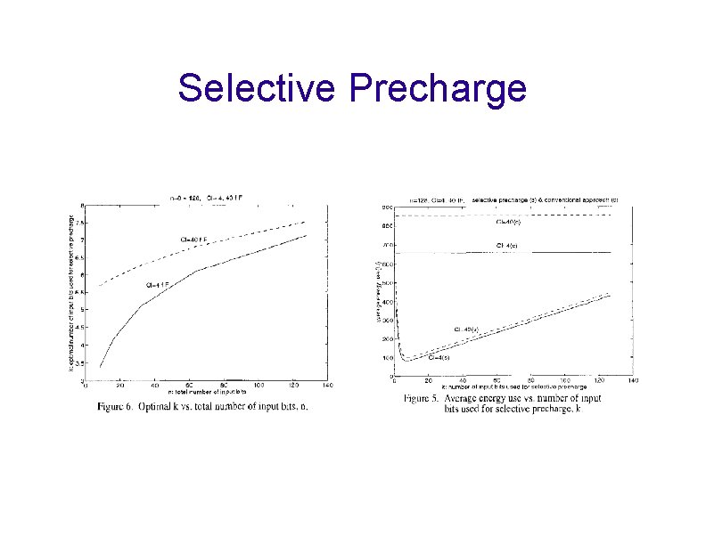
Selective Precharge

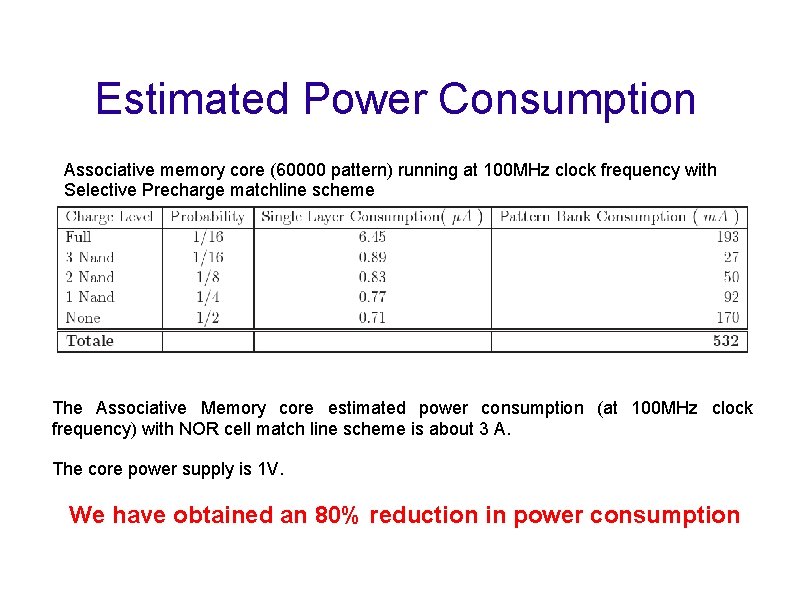
Estimated Power Consumption Associative memory core (60000 pattern) running at 100 MHz clock frequency with Selective Precharge matchline scheme The Associative Memory core estimated power consumption (at 100 MHz clock frequency) with NOR cell match line scheme is about 3 A. The core power supply is 1 V. We have obtained an 80% reduction in power consumption

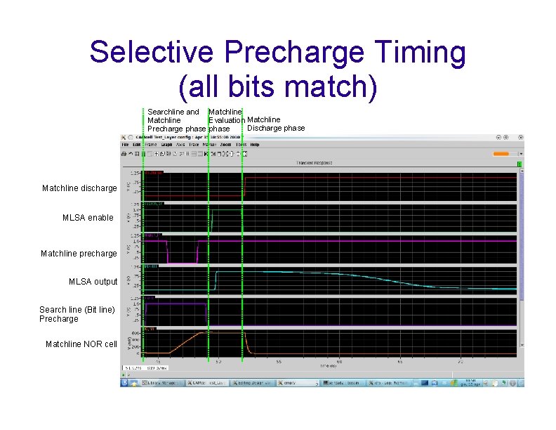
Selective Precharge Timing (all bits match) Searchline and Matchline Evaluation Matchline Discharge phase Precharge phase Matchline discharge MLSA enable Matchline precharge MLSA output Search line (Bit line) Precharge Matchline NOR cell

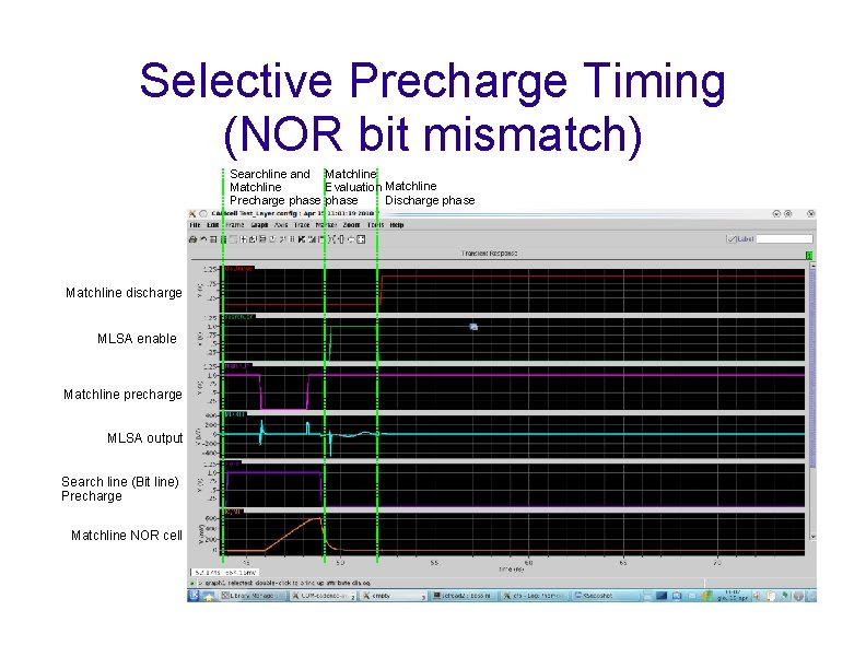
Selective Precharge Timing (NOR bit mismatch) Searchline and Matchline Evaluation Matchline Discharge phase Precharge phase Matchline discharge MLSA enable Matchline precharge MLSA output Search line (Bit line) Precharge Matchline NOR cell

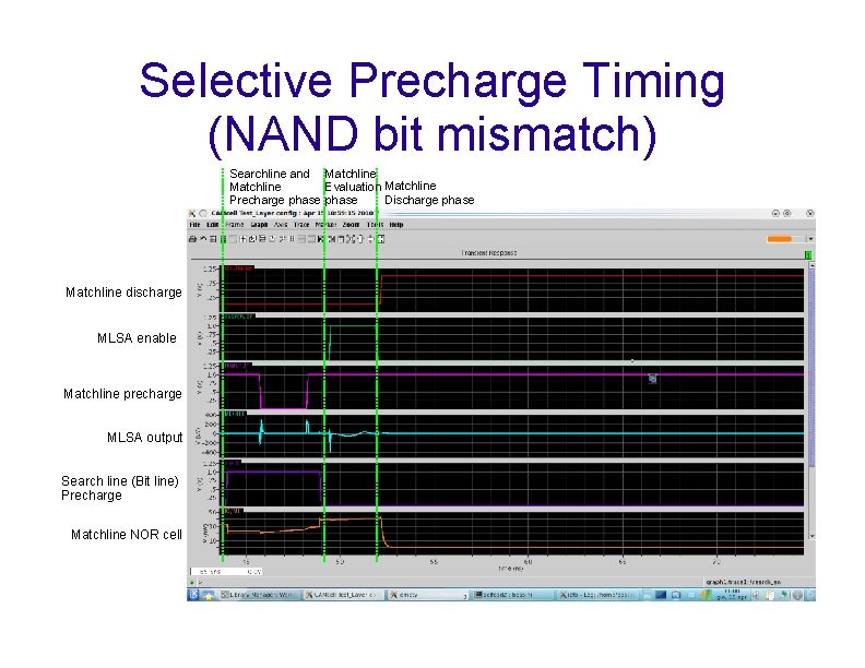
Selective Precharge Timing (NAND bit mismatch) Searchline and Matchline Evaluation Matchline Discharge phase Precharge phase Matchline discharge MLSA enable Matchline precharge MLSA output Search line (Bit line) Precharge Matchline NOR cell

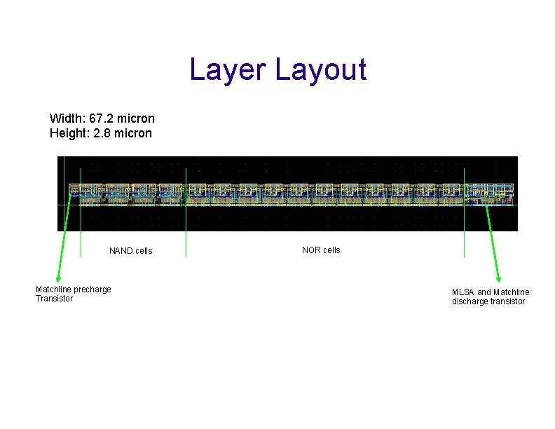
Layer Layout Width: 67. 2 micron Height: 2. 8 micron NAND cells Matchline precharge Transistor NOR cells MLSA and Matchline discharge transistor

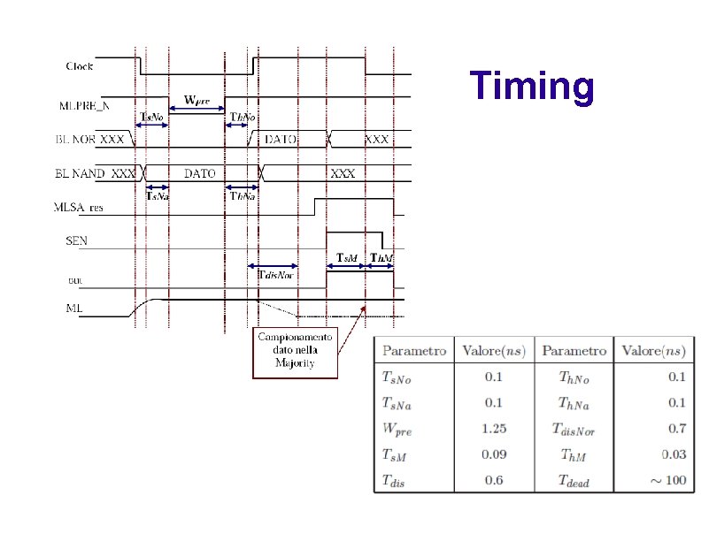
Timing

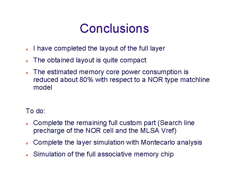
Conclusions I have completed the layout of the full layer The obtained layout is quite compact The estimated memory core power consumption is reduced about 80% with respect to a NOR type matchline model To do: Complete the remaining full custom part (Search line precharge of the NOR cell and the MLSA Vref) Complete the layer simulation with Montecarlo analysis Simulation of the full associative memory chip