
Frequency Scaling and Topology Comparison of Millimeterwave VCOs









- Slides: 20
Frequency Scaling and Topology Comparison of Millimeter-wave VCOs Keith Tang Steven Leung Nelson Tieu Peter Schvan* Sorin Voinigescu University of Toronto, *NORTEL University of Toronto 2006 1
Outline Motivation VCO Design Methodology Frequency Scaling Measurement Summary University of Toronto 2006 2
Motivation MOSFET DC, HF and noise characteristics are scalable across technology nodes VCO topologies are very simple with one or two transistor half-circuits Algorithmic design and frequency scaling methodologies can be developed even at 77 GHz → Design productivity increases! University of Toronto 2006 3
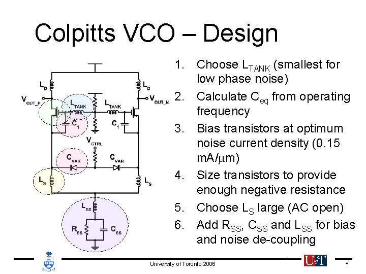
Colpitts VCO – Design 1. Choose LTANK (smallest for low phase noise) 2. Calculate Ceq from operating frequency 3. Bias transistors at optimum noise current density (0. 15 m. A/mm) 4. Size transistors to provide enough negative resistance 5. Choose LS large (AC open) 6. Add RSS, CSS and LSS for bias and noise de-coupling University of Toronto 2006 4
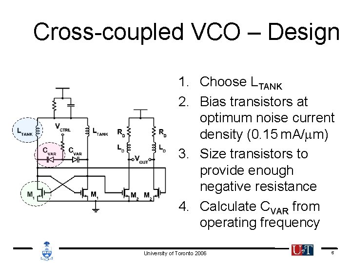
Cross-coupled VCO – Design 1. Choose LTANK 2. Bias transistors at optimum noise current density (0. 15 m. A/mm) 3. Size transistors to provide enough negative resistance 4. Calculate CVAR from operating frequency University of Toronto 2006 5
Frequency Scaling LTANK/k C 1/k k f. OSC CVAR/k Same applies to cross-coupled VCO University of Toronto 2006 6
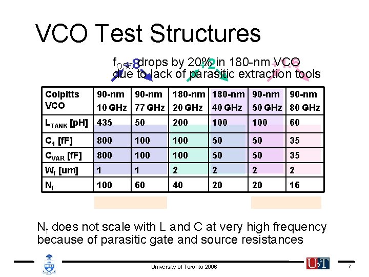
VCO Test Structures f. OSC VCO 8 drops by 20% 2 in 180 -nm 1. 6 due to lack of parasitic extraction tools Colpitts VCO 90 -nm 180 -nm 90 -nm 10 GHz 77 GHz 20 GHz 40 GHz 50 GHz 80 GHz LTANK [p. H] 435 50 200 100 60 C 1 [f. F] 800 100 50 50 35 CVAR [f. F] 800 100 50 50 35 Wf [um] 1 1 2 2 Nf 100 60 40 20 20 16 Nf does not scale with L and C at very high frequency because of parasitic gate and source resistances University of Toronto 2006 7
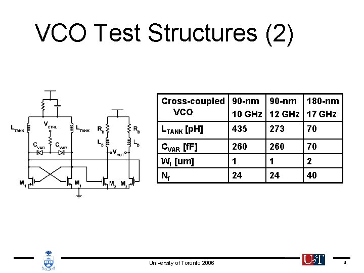
VCO Test Structures (2) Cross-coupled 90 -nm 180 -nm VCO 10 GHz 12 GHz 17 GHz LTANK [p. H] 435 273 70 CVAR [f. F] 260 70 Wf [um] 1 1 2 Nf 24 24 40 University of Toronto 2006 8
10 -GHz Colpitts VCO Tuning range: 9. 2 – 10. 4 GHz (11. 8%) Record phase noise: -117. 5 d. Bc/Hz @ 1 MHz (100 avg. ) University of Toronto 2006 9
77 -GHz Colpitts VCO Record tuning range: 73. 8 – 80. 0 GHz (8. 3%) Record phase noise: -100. 3 d. Bc/Hz @ 1 MHz (100 avg. ) 20 log(8) ≈ 17 d. B higher than 10 -GHz VCO’s phase noise! University of Toronto 2006 10
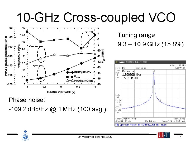
10 -GHz Cross-coupled VCO Tuning range: 9. 3 – 10. 9 GHz (15. 8%) Phase noise: -109. 2 d. Bc/Hz @ 1 MHz (100 avg. ) University of Toronto 2006 11
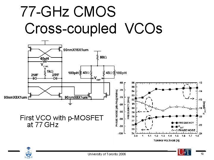
77 -GHz CMOS Cross-coupled VCOs First VCO with p-MOSFET at 77 GHz University of Toronto 2006 12
Die Photos 77 GHz Colpitts VCO: 77 GHz Cross-coupled VCO: 0. 40 mm 0. 16 mm 0. 08 mm 0. 27 mm 0. 22 mm 0. 42 mm 0. 22 mm 0. 37 mm University of Toronto 2006 13
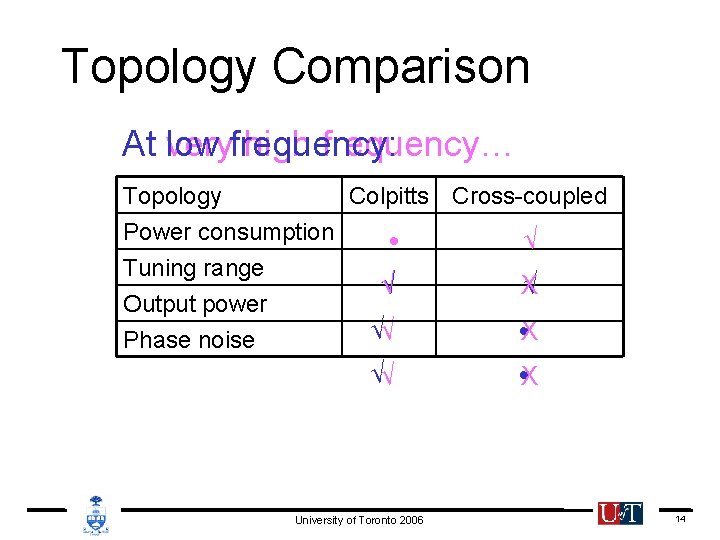
Topology Comparison At low veryfrequency: high frequency… Topology Colpitts Cross-coupled Power consumption ․ √ Tuning range √ X √ Output power Phase noise √√ ․ X University of Toronto 2006 14
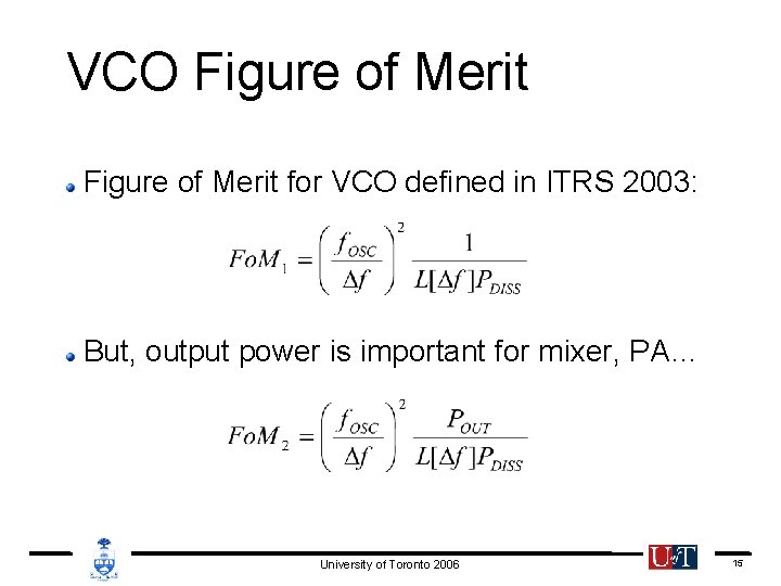
VCO Figure of Merit for VCO defined in ITRS 2003: But, output power is important for mixer, PA… University of Toronto 2006 15
Fo. Ms Comparison With Fo. M 2, Si. Ge HBT VCOs show better performance than CMOS VCOs at mm-wave frequencies University of Toronto 2006 16
Summary VCOs with record-breaking performances achieved by algorithmic design at 10 and 77 GHz Frequency scaling of Colpitts VCOs from 10 to 77 GHz in 90 -nm CMOS, 20 to 40 GHz in 180 -nm CMOS demonstrated First cross-coupled VCO with p-MOSFET at 77 GHz Colpitts topology exhibits better performances than cross-coupled topology at mm-wave frequencies University of Toronto 2006 17
Acknowledgement NORTEL and CMC for fabrication CMC for CAD tools CFI and OIT for test equipment Dr. M. T. Yang for support University of Toronto 2006 18
Loss at Very High Frequency Considering the transistor’s resistance: RG, RS increase with frequency and both lumped to RTANK - Larger transistor size required at very high frequencies It is critical to keep the VCO layout identical: - Transistor layout Component orientation Interconnect routing such that layout parasitics also scale University of Toronto 2006 19
Ref Process fosc [GHz] Tuning [%] Phase Noise [d. Bc/Hz] Pout [d. Bm] Pdiss [m. W] Fo. M 1 [d. B] Fo. M 2 [d. B] * 90 -nm CMOS: Colpitts 10 12. 2 -117. 5@1 MHz 4. 0 36 181. 9 185. 9 77 8. 1 -100. 3@1 MHz -13. 8 37. 5 182. 3 168. 5 * NMOS cross-coupled 10 15. 8 -109. 2@1 MHz -2. 2 7. 5 180. 4 178. 2 * CMOS cross-coupled 77 2. 6 -84. 3@10 MHz -13. 2 13. 5 150. 7 137. 5 [1] 90 -nm CMOS 60 0. 17 -100@1 MHz -23. 2 1. 9 192. 8 169. 6 *[6] Si. Ge HBT, f. T = 170 GHz 96 4. 6 -101. 6@1 MHz 0. 7 133 180. 0 180. 7 Si. Ge HBT, f. T = 230 GHz 105 4. 4 -101. 3@1 MHz 2. 7 133 180. 3 183. 0 Si. Ge HBT, f. T = 175 GHz 77 8. 7 -97@1 MHz 18. 5 1200 163. 9 183. 0 100 6. 2 -90@1 MHz 14. 3 1200 159. 2 173. 5 [7] [8] Si. Ge HBT, f. T = 200 GHz 75 6. 1 -105@1 MHz 3. 5 72 183. 9 187. 4 [9] Si. Ge HBT, f. T = 200 GHz 98 3. 3 -85@1 MHz -6 60 167. 0 161. 0 [10] Si. Ge HBT, f. T = 200 GHz 85 2. 7 -94@1 MHz -8 25 178. 6 170. 6 [11] In. P HBT, f. T = 75 GHz 108 2. 6 -88@1 MHz 0. 92 204 165. 6 166. 5 [12] 130 nm CMOS 90 2. 4 -105@10 MHz -16 15. 5 172. 2 156. 2 [13] 130 nm CMOS 114 2. 1 -107. 6@10 MHz -22. 5 8. 4 179. 5 157. 0 * our work University of Toronto 2006 20