FPLDS Introduction What is Programmable Logic Circa 1970

FPLDS Introduction
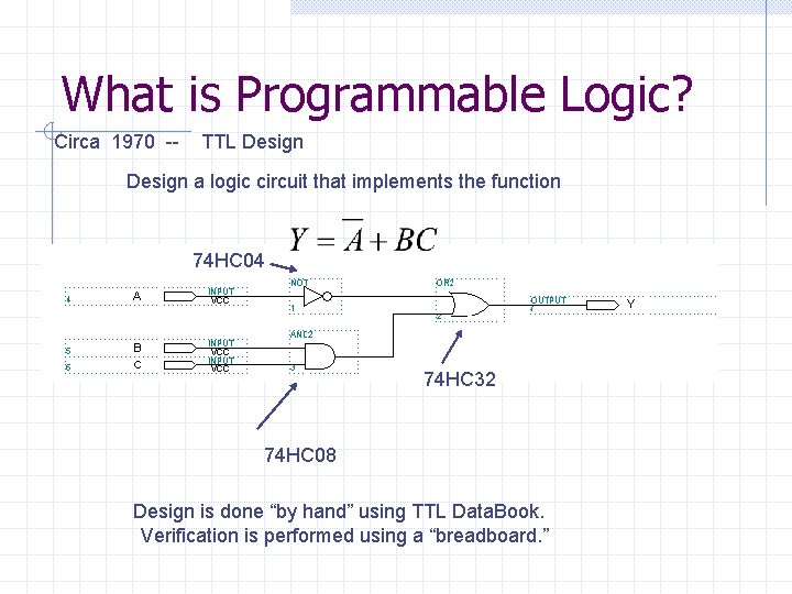
What is Programmable Logic? Circa 1970 -- TTL Design a logic circuit that implements the function 74 HC 04 74 HC 32 74 HC 08 Design is done “by hand” using TTL Data. Book. Verification is performed using a “breadboard. ”
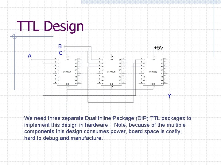
TTL Design We need three separate Dual Inline Package (DIP) TTL packages to implement this design in hardware. Note, because of the multiple components this design consumes power, board space is costly, hard to debug and manufacture.

FPLD Design In field programmable logic device (FPLD) design (FPLD), we use a computer aided design (CAD) software tool (e. g. QUARTUS II) to perform “design entry. ” We can also use the same package for “design verification” and also to “download” the “design program” into hardware (i. e. the PLD). Our design now becomes: This single chip design requires Less power, less board space, should cost less on a per gate basis, is easier to debug (in software), and be easier to manufacture. Also, Intellectual Property (IP) can be protected and exploited using a FPLD.
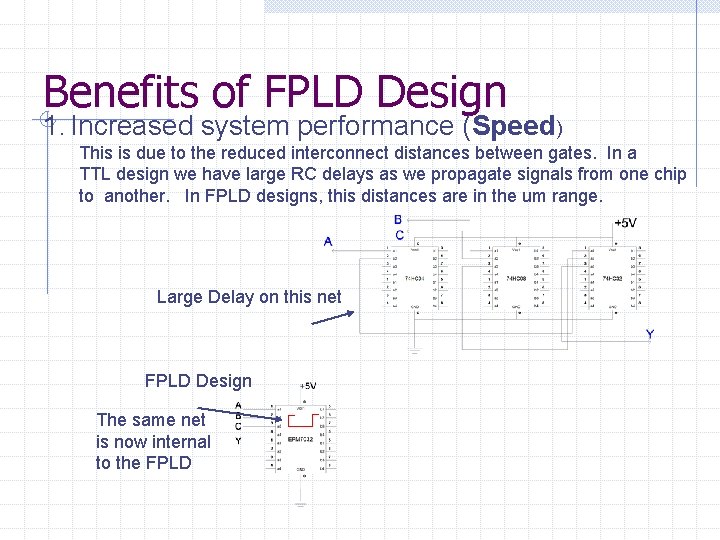
Benefits of FPLD Design 1. Increased system performance (Speed) This is due to the reduced interconnect distances between gates. In a TTL design we have large RC delays as we propagate signals from one chip to another. In FPLD designs, this distances are in the um range. Large Delay on this net FPLD Design The same net is now internal to the FPLD

Benefits of FPLD Design 2. Increased Gate Density More logic gates on each FPLD implies that you can have more functionality per unit area of board space. A single FPLDs/FPGAs can hold the equivalent of over 1 million TTL logic gates. 3. Reduced Development Time CAD tools significantly reduce the development time for new designs. This not only cuts down the “time to market, ” but also allows reduces the size of the team needed to complete a design.
Benefits of FPLD Design 4. Rapid Hardware Prototyping Hardware prototyping is greatly simplified using FPLDs because it is relatively easy to change the design. One major concern however is I/O pin assignments. 5. Reduced “Time to Market” Since FPLDs are already “complete, ” there is no need to wait for fabrication.
Benefits of FPLD Design 6. Future Modifications Since FPLDs can be “reconfigured” in the field. It is possible to have the end user perform system “upgrades. ” 7. Reduced Inventory Risk The same type of FPLD can be used in multiple designs, so the inventory risk is significantly reduced.

Benefits of FPLD Design 8. Reduced Development Costs The development costs for FPLDs tend to be lower than Application Specific Integrated Circuits (ASICs); however, the per unit cost of a FPLD is higher than an ASIC for large volumes.
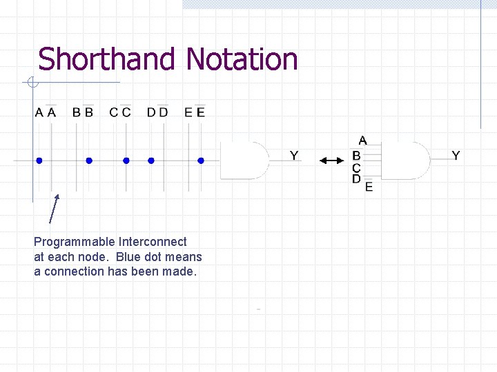
Shorthand Notation Programmable Interconnect at each node. Blue dot means a connection has been made.
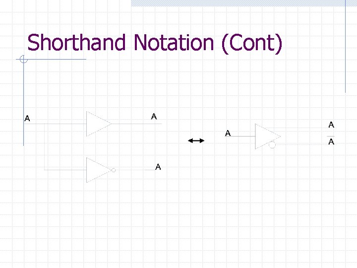
Shorthand Notation (Cont)
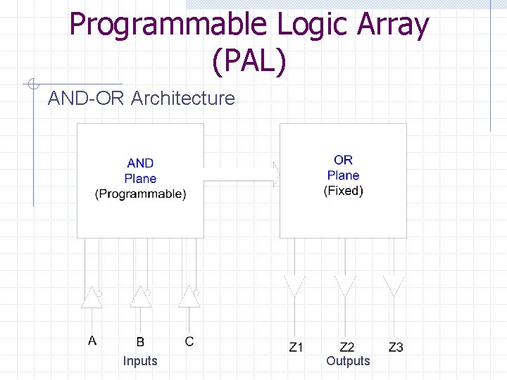
Programmable Logic Array (PAL) AND-OR Architecture Inputs Outputs
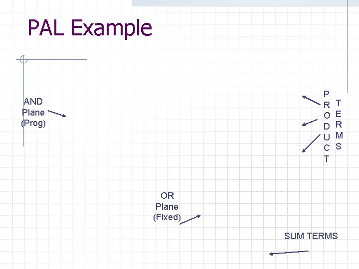
PAL Example P R O D U C T AND Plane (Prog) T E R M S OR Plane (Fixed) SUM TERMS
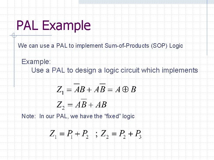
PAL Example We can use a PAL to implement Sum-of-Products (SOP) Logic Example: Use a PAL to design a logic circuit which implements Note: In our PAL, we have the “fixed” logic
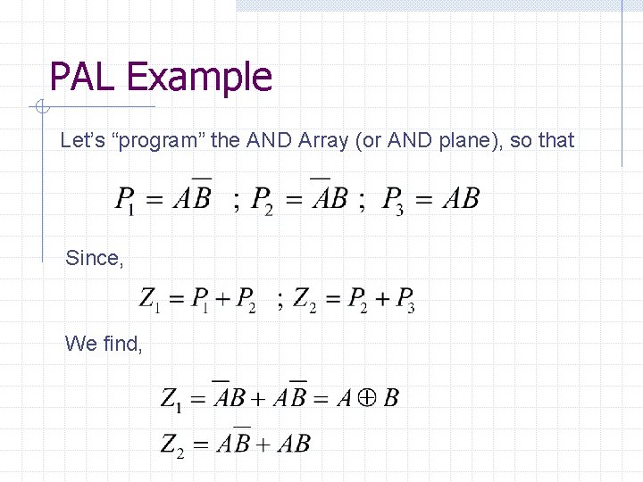
PAL Example Let’s “program” the AND Array (or AND plane), so that Since, We find,
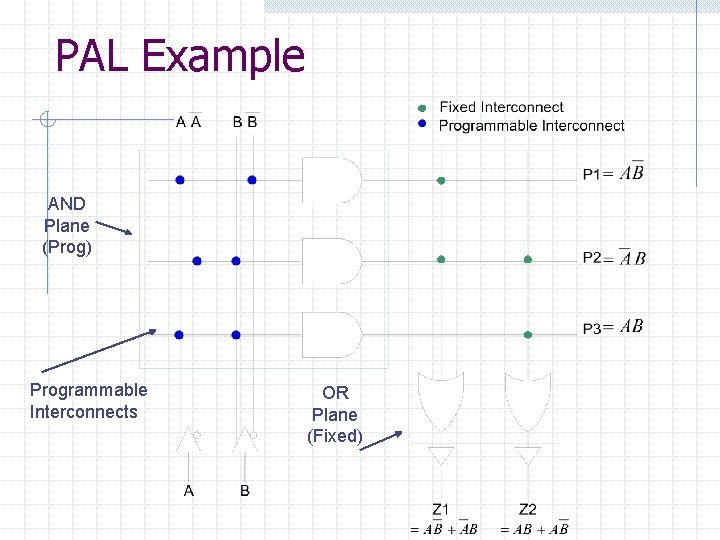
PAL Example AND Plane (Prog) Programmable Interconnects OR Plane (Fixed)
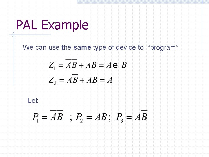
PAL Example We can use the same type of device to “program” Let
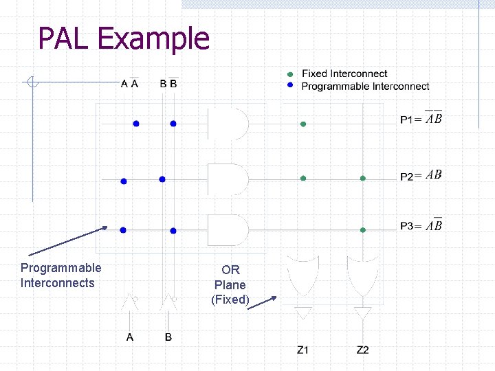
PAL Example Programmable Interconnects OR Plane (Fixed)

PAL Example However, what if, I want Let What about term? I’ve run out of pterms!!! Need to pick a bigger PAL!!!
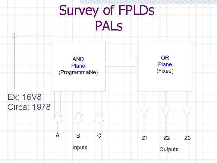
Survey of FPLDs PALs Ex: 16 V 8 Circa: 1978 Inputs Outputs
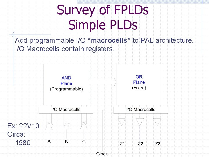
Survey of FPLDs Simple PLDs Add programmable I/O “macrocells” to PAL architecture. I/O Macrocells contain registers. Ex: 22 V 10 Circa: 1980
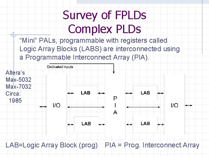
Survey of FPLDs Complex PLDs “Mini” PALs, programmable with registers called Logic Array Blocks (LABS) are interconnected using a Programmable Interconnect Array (PIA). Altera’s Max-5032 Max-7032 Circa: 1985 LAB=Logic Array Block (prog) PIA = Prog. Interconnect Array
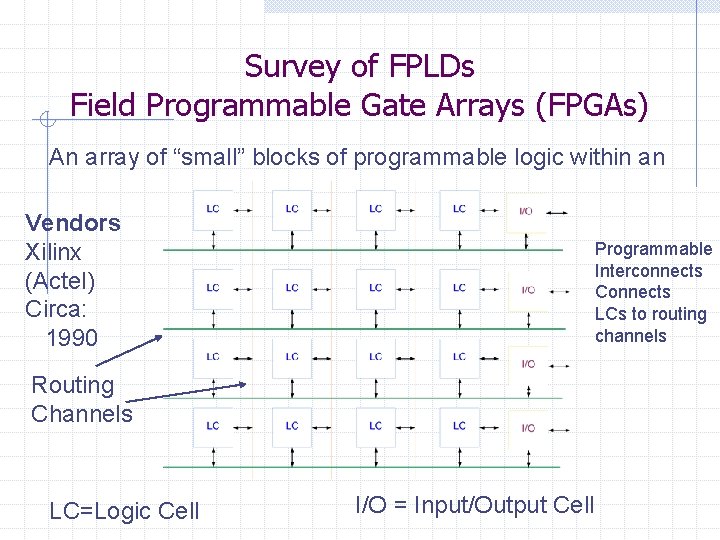
Survey of FPLDs Field Programmable Gate Arrays (FPGAs) An array of “small” blocks of programmable logic within an Vendors Xilinx (Actel) Circa: 1990 Programmable Interconnects Connects LCs to routing channels Routing Channels LC=Logic Cell I/O = Input/Output Cell
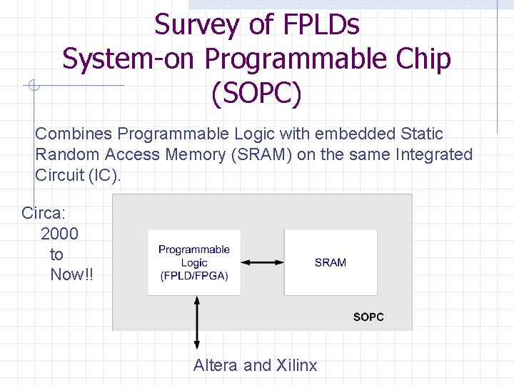
Survey of FPLDs System-on Programmable Chip (SOPC) Combines Programmable Logic with embedded Static Random Access Memory (SRAM) on the same Integrated Circuit (IC). Circa: 2000 to Now!! Altera and Xilinx
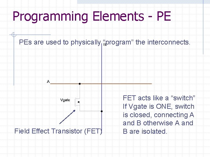
Programming Elements - PE PEs are used to physically “program” the interconnects. Field Effect Transistor (FET) FET acts like a “switch” If Vgate is ONE, switch is closed, connecting A and B otherwise A and B are isolated.
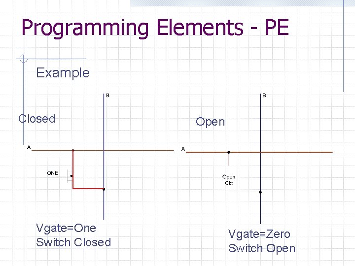
Programming Elements - PE Example Closed Vgate=One Switch Closed Open Vgate=Zero Switch Open

Programming Elements - PE So, we’ll have one FET at every programmable Interconnect, but we need a method or technique to “program” VGATE to be ONE or ZERO. Before, we look at our options, some definitions
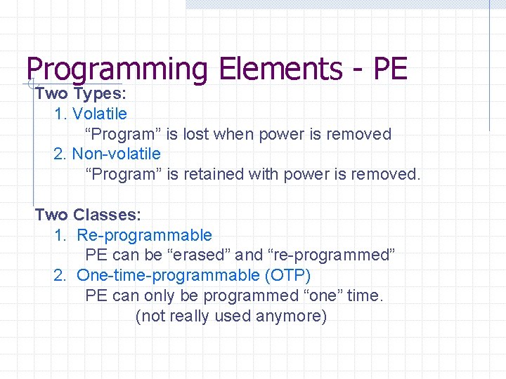
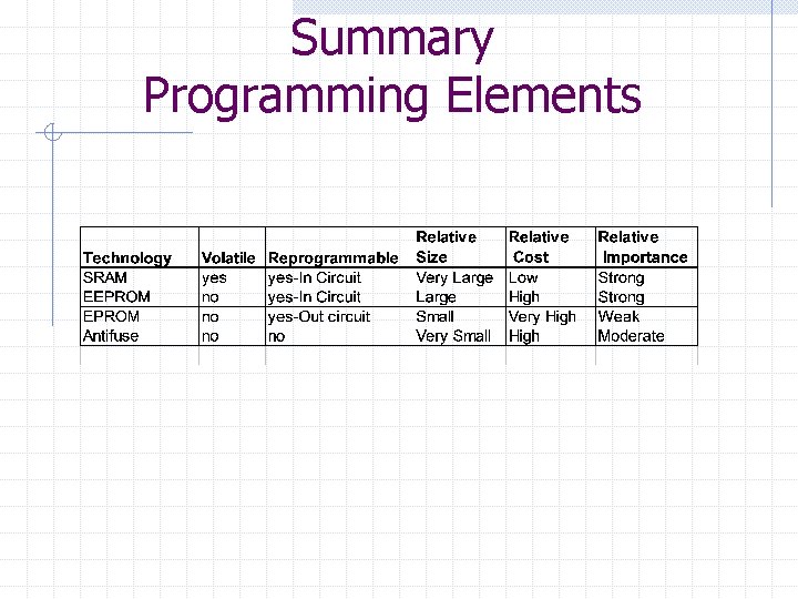
Programming Elements - PE Two Types: 1. Volatile “Program” is lost when power is removed 2. Non-volatile “Program” is retained with power is removed. Two Classes: 1. Re-programmable PE can be “erased” and “re-programmed” 2. One-time-programmable (OTP) PE can only be programmed “one” time. (not really used anymore)
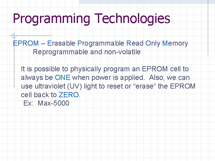
Programming Technologies EPROM – Erasable Programmable Read Only Memory Reprogrammable and non-volatile It is possible to physically program an EPROM cell to always be ONE when power is applied. Also, we can use ultraviolet (UV) light to reset or “erase” the EPROM cell back to ZERO. Ex: Max-5000
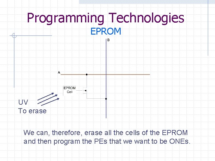
Programming Technologies EPROM UV To erase We can, therefore, erase all the cells of the EPROM and then program the PEs that we want to be ONEs.
Programming Technologies EEPROM – (E 2 PROM) Electrically Erasable Programmable Read Only Memory Reprogrammable and non-volatile Similar to an EPROM except cell can be “erased” electrically. Ex: MAX-7000 family
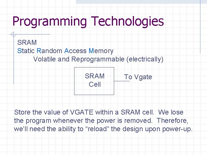
Programming Technologies SRAM Static Random Access Memory Volatile and Reprogrammable (electrically) SRAM Cell To Vgate Store the value of VGATE within a SRAM cell. We lose the program whenever the power is removed. Therefore, we’ll need the ability to “reload” the design upon power-up.
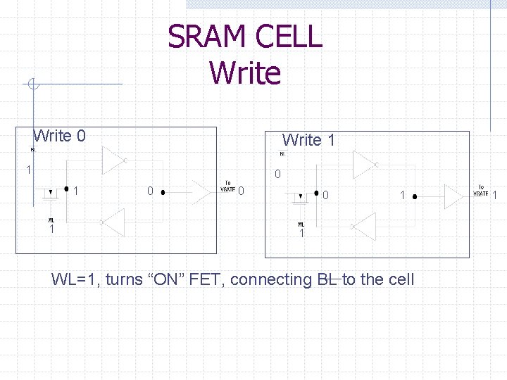
SRAM CELL Write 0 Write 1 1 0 0 0 1 1 WL=1, turns “ON” FET, connecting BL to the cell 1
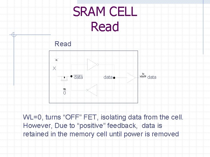
SRAM CELL Read X data 0 WL=0, turns “OFF” FET, isolating data from the cell. However, Due to “positive” feedback, data is retained in the memory cell until power is removed
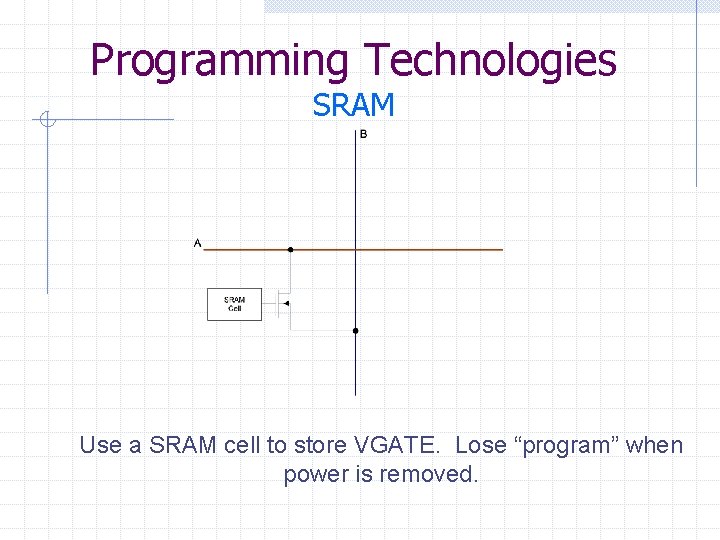
Programming Technologies SRAM Use a SRAM cell to store VGATE. Lose “program” when power is removed.

Programming Technologies Anti-Fuse Non-volatile and OTP Normally, anti-fuse behaves like an “open” circuit, however you can “destroy” the fuse electrically so that it behaves like a short circuit. Anti-fuse. The antifuse is very small compared to the other PEs.
Summary FPLD Benefits 1. 2. 3. 4. 5. 6. 7. 8. Increased Performance Increased Gate Density Reduced Development Time Rapid Hardware Prototyping Reduced “Time to Market” Future Modifications Reduced Inventory Risks Reduced Development Costs
Summary FPLD Types 1. PALS 2. Simple PLDs 3. Complex PLDs (FPLDs) 4. FPGAs 5. SOPC
Summary Programming Elements Types: Classes: 1. Volatile 2. Non-Volatile 1. Reprogrammable 2. OTP Technologies: 1. EPROM (Obsolete) 2. EEPROM 3. Anti-Fuse 4. SRAM
Summary Programming Elements
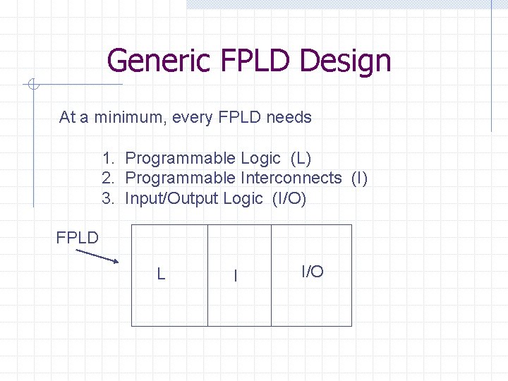
Generic FPLD Design At a minimum, every FPLD needs 1. Programmable Logic (L) 2. Programmable Interconnects (I) 3. Input/Output Logic (I/O) FPLD L I I/O
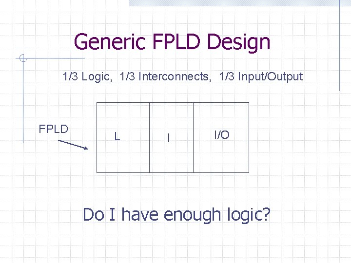
Generic FPLD Design 1/3 Logic, 1/3 Interconnects, 1/3 Input/Output FPLD L I I/O Do I have enough logic?

Generic FPLD Design 1/2 Logic, 1/4 Interconnects, 1/4 Input/Output FPLD L I I/O Logic is good, but now do I have enough interconnects for my logic?
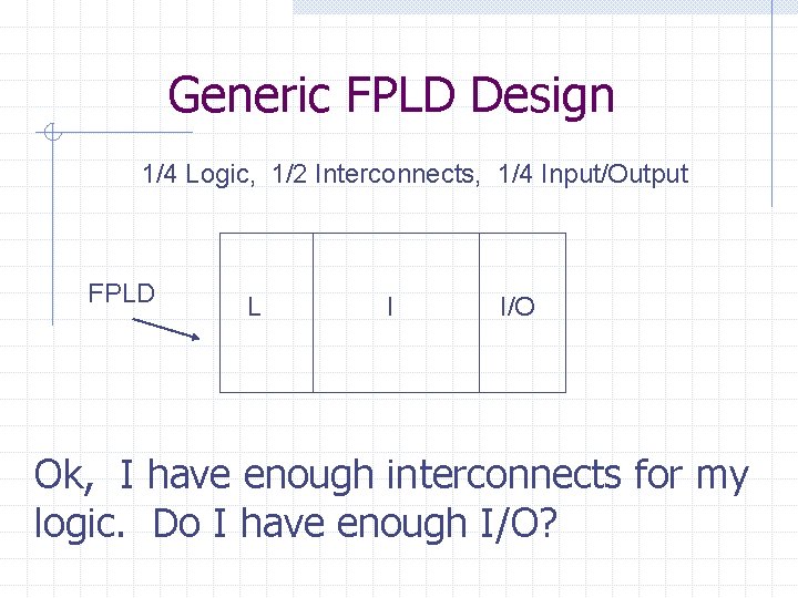
Generic FPLD Design 1/4 Logic, 1/2 Interconnects, 1/4 Input/Output FPLD L I I/O Ok, I have enough interconnects for my logic. Do I have enough I/O?
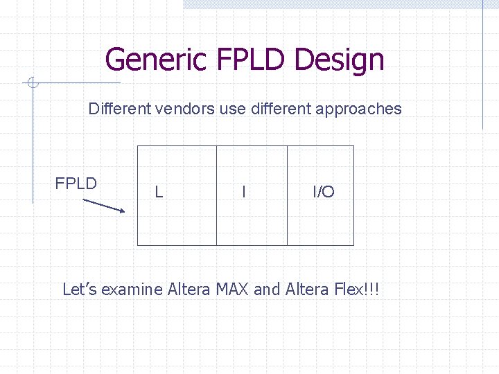
Generic FPLD Design Different vendors use different approaches FPLD L I I/O Let’s examine Altera MAX and Altera Flex!!!
Altera Max-7000
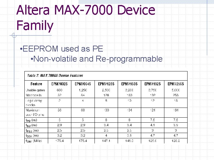
Altera MAX-7000 Device Family • EEPROM used as PE • Non-volatile and Re-programmable
Definitions Useable gates n Number of equivalent TTL NAND gates Macrocells n Number of unique mini PALs Maximum user I/O Pins Tpd = Input to non-registered output Tsu = External global clock register setup time Tfsu = External fast input register setup time Tco 1 = Global clock to output delay Fcnt (MHz) = Maximum 16 bit up/down counter freq
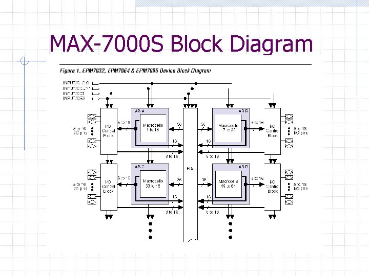
MAX-7000 S Block Diagram
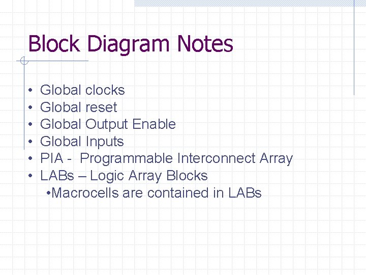
Block Diagram Notes • • • Global clocks Global reset Global Output Enable Global Inputs PIA - Programmable Interconnect Array LABs – Logic Array Blocks • Macrocells are contained in LABs
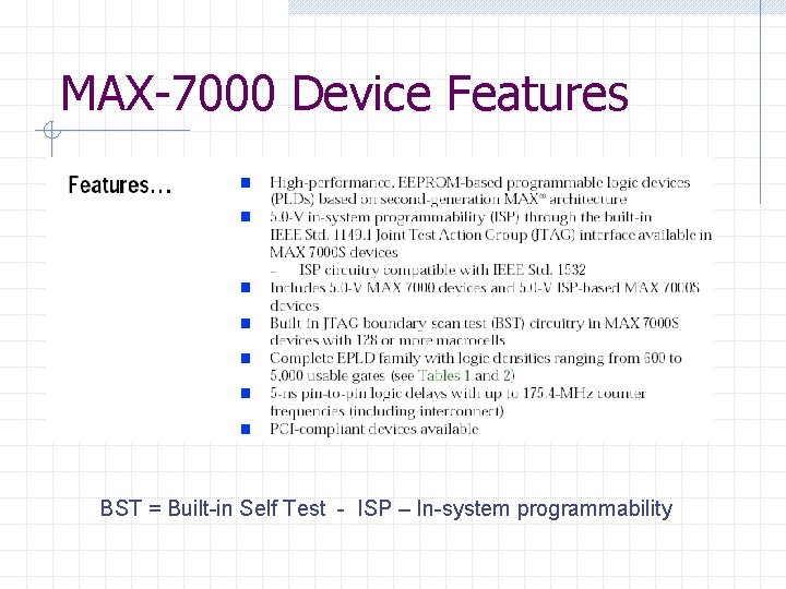
MAX-7000 Device Features BST = Built-in Self Test - ISP – In-system programmability

MAX-7000 Features (cont)
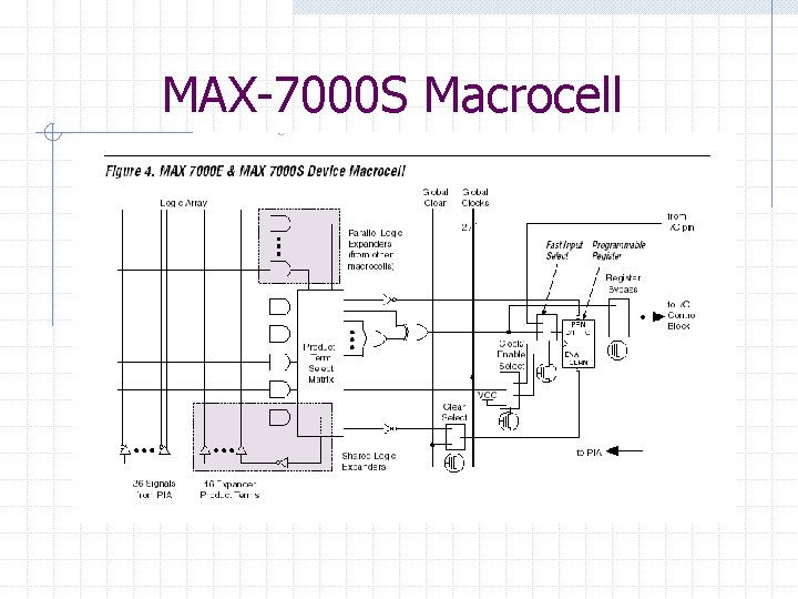
MAX-7000 S Macrocell
Macrocell Notes Macrocell is customizable Local and Global Clocks n Global clock used if no logic added to clock line Register bypass for combinational logic designs One programmable register per MC n n n D, T, JK or SR operation Enable function Preset and reset functions Sharable expanders allow extra pterm to be “shared” with another macrocell
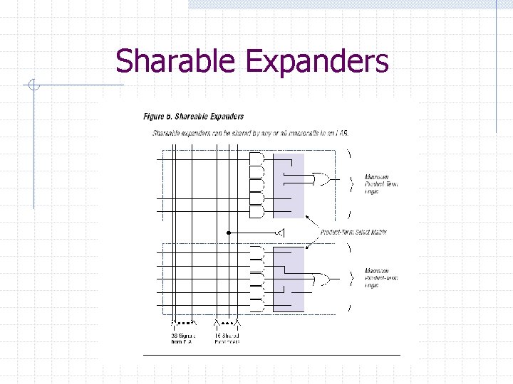
Sharable Expanders
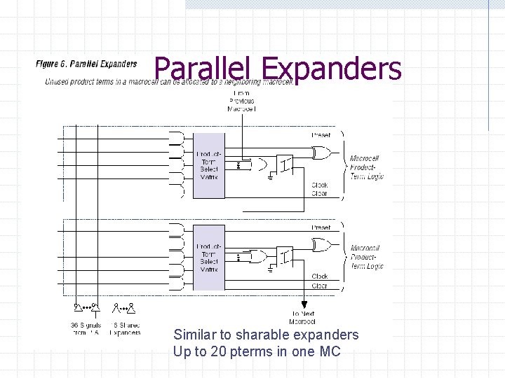
Parallel Expanders Similar to sharable expanders Up to 20 pterms in one MC

Altera Flex 10 K
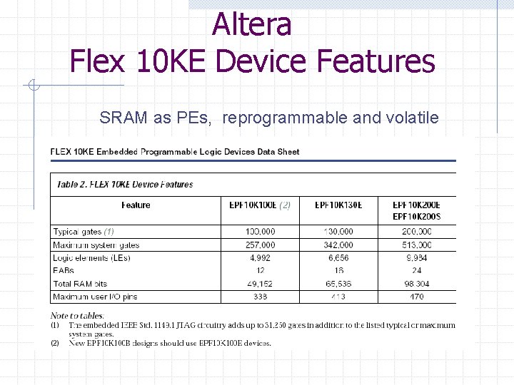
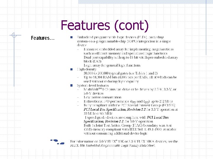
Altera Flex 10 KE Device Features SRAM as PEs, reprogrammable and volatile
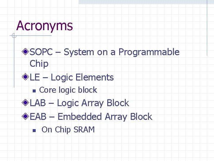
Acronyms SOPC – System on a Programmable Chip LE – Logic Elements n Core logic block LAB – Logic Array Block EAB – Embedded Array Block n On Chip SRAM
Features (cont)
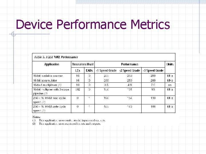
Device Performance Metrics
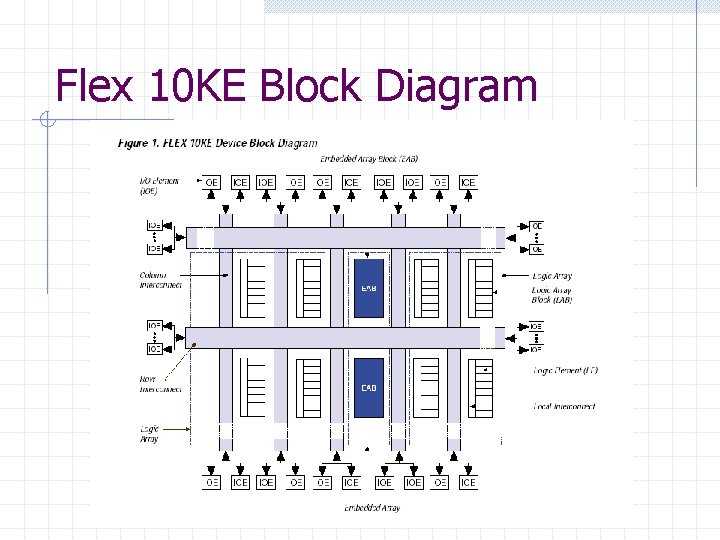
Flex 10 KE Block Diagram

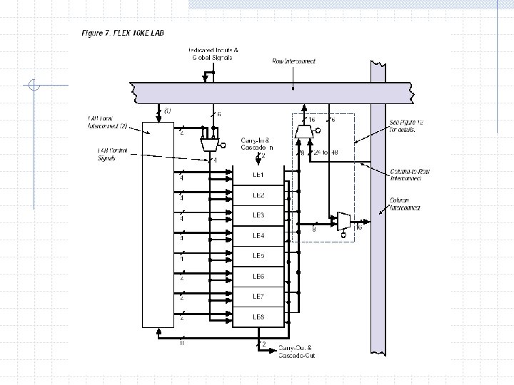
Block Diagram Notes Still have LABs, but MC replaced with LE n Each LAB has eight (8) LEs Embedded memory stored in EABs n Asynchronous and Synchronous modes
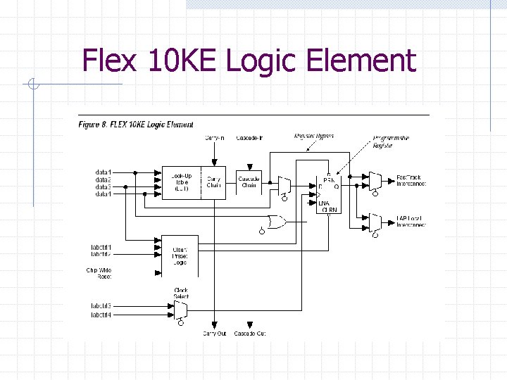
Flex 10 KE Logic Element
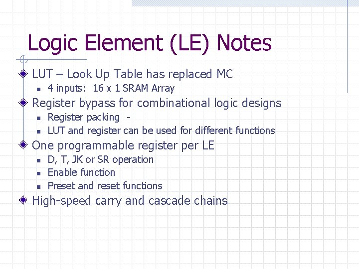
Logic Element (LE) Notes LUT – Look Up Table has replaced MC n 4 inputs: 16 x 1 SRAM Array Register bypass for combinational logic designs n n Register packing LUT and register can be used for different functions One programmable register per LE n n n D, T, JK or SR operation Enable function Preset and reset functions High-speed carry and cascade chains

Look Up Tables (LUTS)
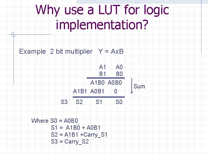
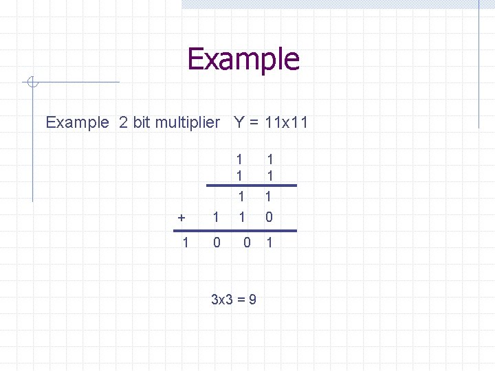
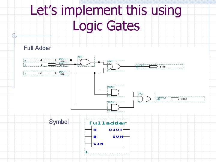
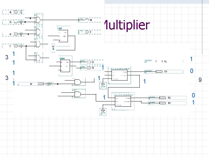
Why use a LUT for logic implementation? Example 2 bit multiplier Y = Ax. B A 1 A 0 B 1 B 0 A 1 B 0 A 0 B 0 A 1 B 1 A 0 B 1 0 S 3 S 2 S 1 Where S 0 = A 0 B 0 S 1 = A 1 B 0 + A 0 B 1 S 2 = A 1 B 1 +Carry_S 1 S 3 = Carry_S 2 S 0 Sum
Example 2 bit multiplier Y = 11 x 11 + 1 1 0 3 x 3 = 9 1 1 1 0 1
Let’s implement this using Logic Gates Full Adder Symbol
2 x 2 Bit Multiplier 3 3 1 1 1 1 0 9 1 1 0 1

Same Design using a LUT = Look Up Table A 1 S 3 A 0 S 2 B 1 B 0 LUT 16 x 4 S 1 S 0 Outputs Inputs LUT contains the “Truth table” of the design
![LUT Design A[1. . 0] S[3. . 0] B[1. . 0] LUT Design A[1. . 0] S[3. . 0] B[1. . 0]](http://slidetodoc.com/presentation_image_h2/ec2c785e91210871752b7569b66471c2/image-73.jpg)
LUT Design A[1. . 0] S[3. . 0] B[1. . 0]
![LUT Example Let A=11 and B=11 A[1. . 0]=11 B[1. . 0]=11 S[3. . LUT Example Let A=11 and B=11 A[1. . 0]=11 B[1. . 0]=11 S[3. .](http://slidetodoc.com/presentation_image_h2/ec2c785e91210871752b7569b66471c2/image-74.jpg)
LUT Example Let A=11 and B=11 A[1. . 0]=11 B[1. . 0]=11 S[3. . 0]=1001
2 x 2 Bit Multiplier Delay Calculation Worst Case Delay = tgate + 2*tfa
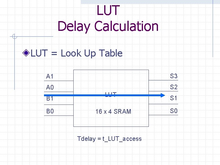
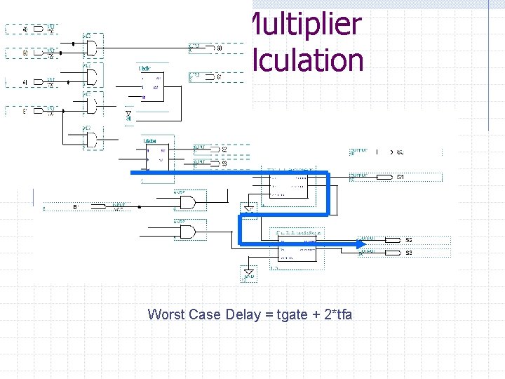
LUT Delay Calculation LUT = Look Up Table A 1 S 3 A 0 S 2 B 1 B 0 LUT 16 x 4 SRAM Tdelay = t_LUT_access S 1 S 0
. Memory Arrays
Memory Arrays We can combine memory cells into memory arrays. Memory arrays used to store n n n State information Data information Startup information
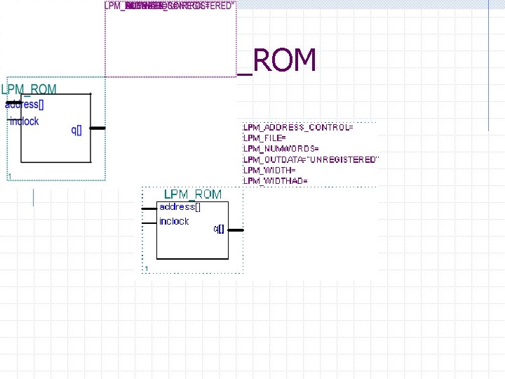
Linear Parameterized Modules LPMs Quartus allows access to EABs through the use of Linear Parameterized Modules (LPMs). Let’s look at various memory arrays available through Quartus.
Memory Arrays Read-Only Memory (ROM) Single Port SRAM Dual Port SRAM First-in First-out (FIFO) SRAM Last-in First-out (LIFO) “Stack” Content Addressable Memory (CAM)
ROMs
Read Only Memory (ROM) A ROM has “pre-loaded” data that is not intended to change overtime. Traditionally, ROMs are used to store program code in a computer system. However, we can also use a ROM as a giant look-up table (LUT) to perform functional translations on our data. There are two basic access modes we will need to examine: 1. Asynchronous mode 2. Synchronous mode
LPM_ROM Implementation Asynchronous mode X Y
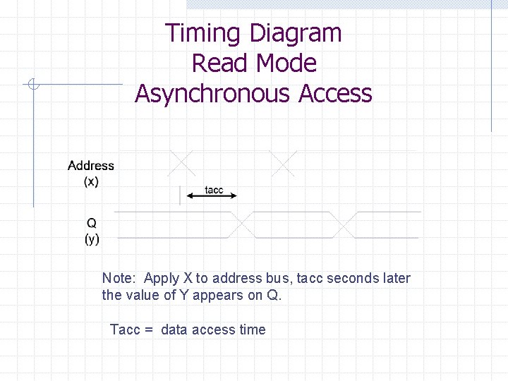
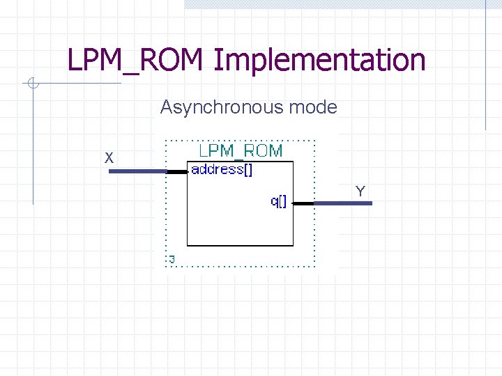
Timing Diagram Read Mode Asynchronous Access Note: Apply X to address bus, tacc seconds later the value of Y appears on Q. Tacc = data access time
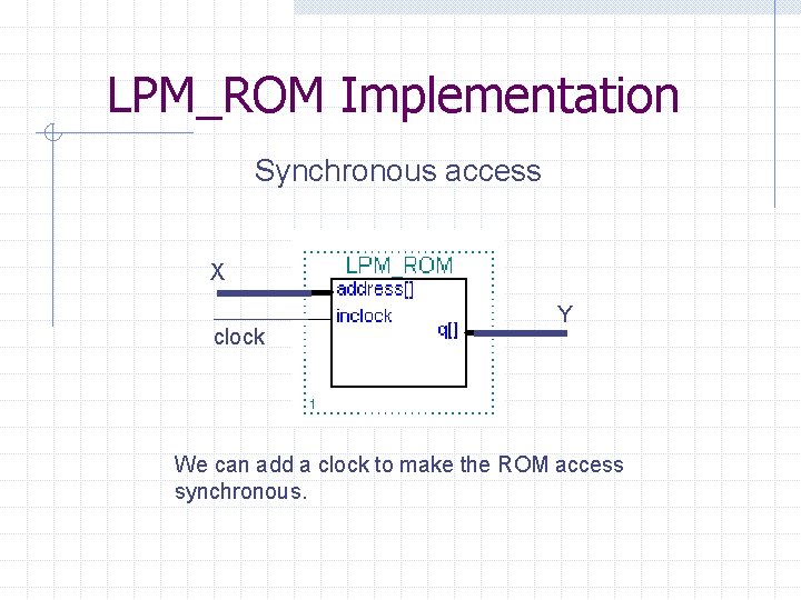
LPM_ROM Implementation Synchronous access X clock Y We can add a clock to make the ROM access synchronous.
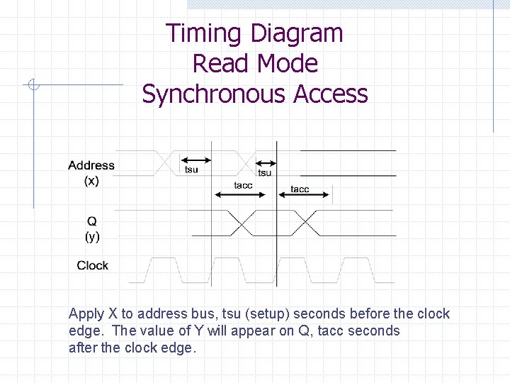
Timing Diagram Read Mode Synchronous Access Apply X to address bus, tsu (setup) seconds before the clock edge. The value of Y will appear on Q, tacc seconds after the clock edge.
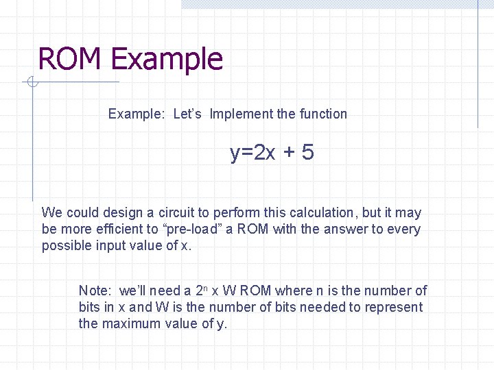
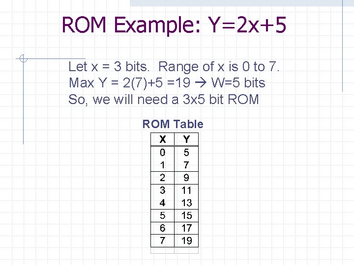
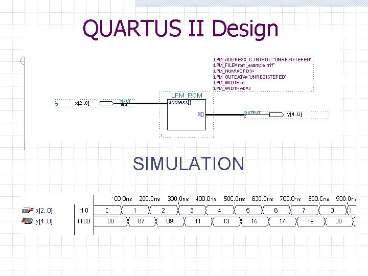
ROM Example: Let’s Implement the function y=2 x + 5 We could design a circuit to perform this calculation, but it may be more efficient to “pre-load” a ROM with the answer to every possible input value of x. Note: we’ll need a 2 n x W ROM where n is the number of bits in x and W is the number of bits needed to represent the maximum value of y.
ROM Example: Y=2 x+5 Let x = 3 bits. Range of x is 0 to 7. Max Y = 2(7)+5 =19 W=5 bits So, we will need a 3 x 5 bit ROM Table
LPM_ROM
QUARTUS II Design SIMULATION
Single Port SRAM
Single Port SRAM A single port SRAM allows data to be read and written into the memory array by the user. In general a single port has the following input/output lines: 1. Data Input bus 2. Data Output bus 3. R/W Control line 4. Address bus The control line is needed to determine which access mode we will need. This can be read mode or write mode. Single port means we use a single port to interface to the RAM
![Static Random Access Memory (SRAM) Array Symbol Data Input Bus Din[n-1. . 0] Data Static Random Access Memory (SRAM) Array Symbol Data Input Bus Din[n-1. . 0] Data](http://slidetodoc.com/presentation_image_h2/ec2c785e91210871752b7569b66471c2/image-93.jpg)
Static Random Access Memory (SRAM) Array Symbol Data Input Bus Din[n-1. . 0] Data Output Bus Add[n-1. . 0] Address Bus Dout[n-1. . 0] R/W Read/Write Control Line R/W = 1 : Read mode R/W = 0 : Write mode Let’s look at an internal block diagram of the SRAM
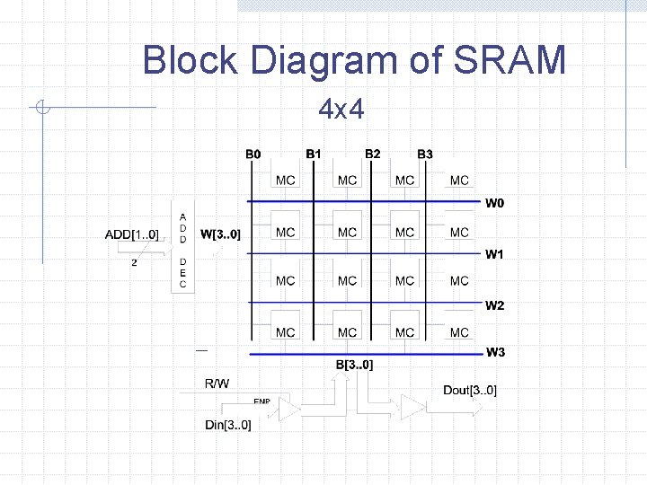
Block Diagram of SRAM 4 x 4
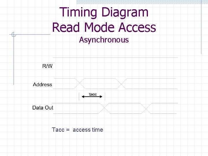
Timing Diagram Read Mode Access Asynchronous Tacc = access time
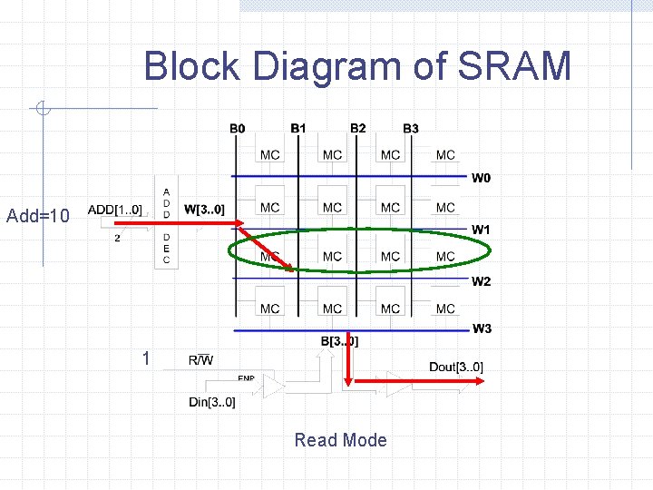
Block Diagram of SRAM Add=10 1 Read Mode
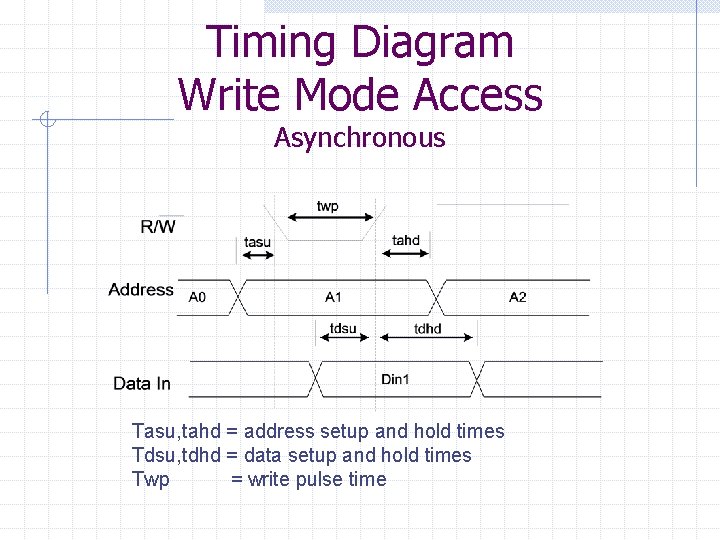
Timing Diagram Write Mode Access Asynchronous Tasu, tahd = address setup and hold times Tdsu, tdhd = data setup and hold times Twp = write pulse time
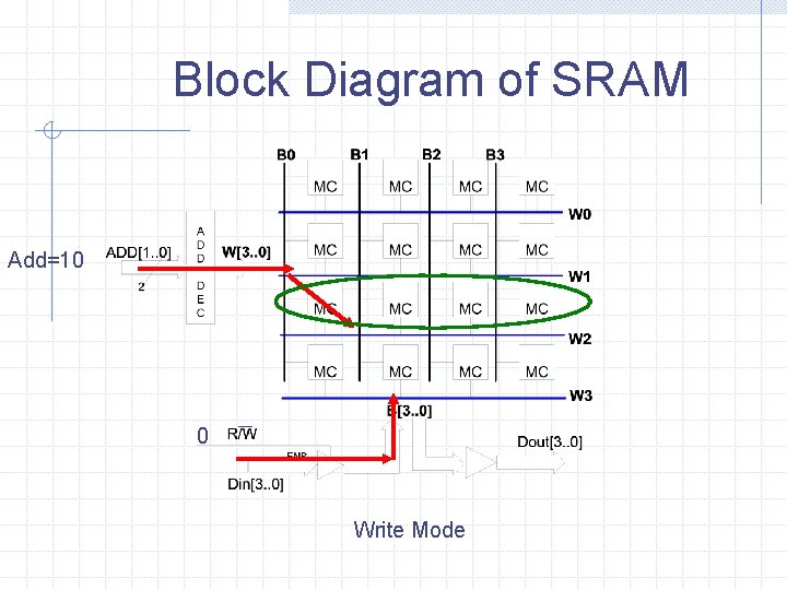
Block Diagram of SRAM Add=10 0 Write Mode
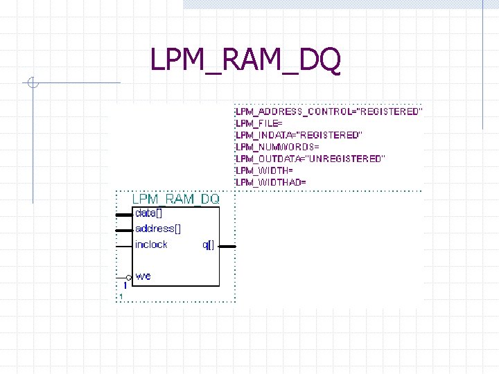
LPM_RAM_DQ
Dual Port SRAM
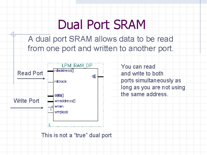
Dual Port SRAM A dual port SRAM allows data to be read from one port and written to another port. Read Port Write Port This is not a “true” dual port You can read and write to both ports simultaneously as long as you are not using the same address.

FIFO First-in First-out Buffer
FIFO Buffer A first-in first-out (FIFO) buffer is used to synchronize two data streams that are processing data at different rates. Note: the “average” data rates of both sides have to be equivalent. As the name implies, the first data byte written on the input side(First-in) is the first data byte read on the output side (First-out).
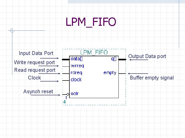
LPM_FIFO Input Data Port Write request port Read request port Clock Asynch reset Output Data port Buffer empty signal

Content Addressable Memory (CAM)
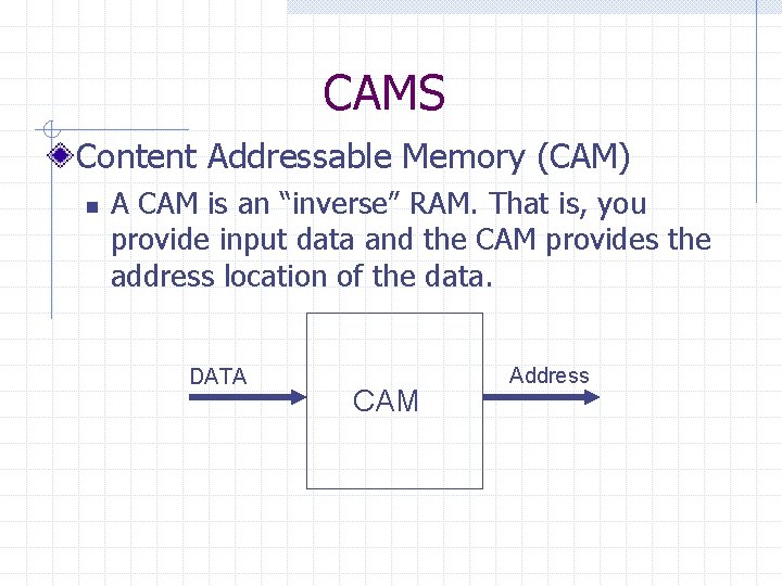
CAMS Content Addressable Memory (CAM) n A CAM is an “inverse” RAM. That is, you provide input data and the CAM provides the address location of the data. DATA CAM Address
- Slides: 106