FPGA Implementation of Multicore AES 128192256 By William
FPGA Implementation of Multicore AES 128/192/256 By: William Whitehouse
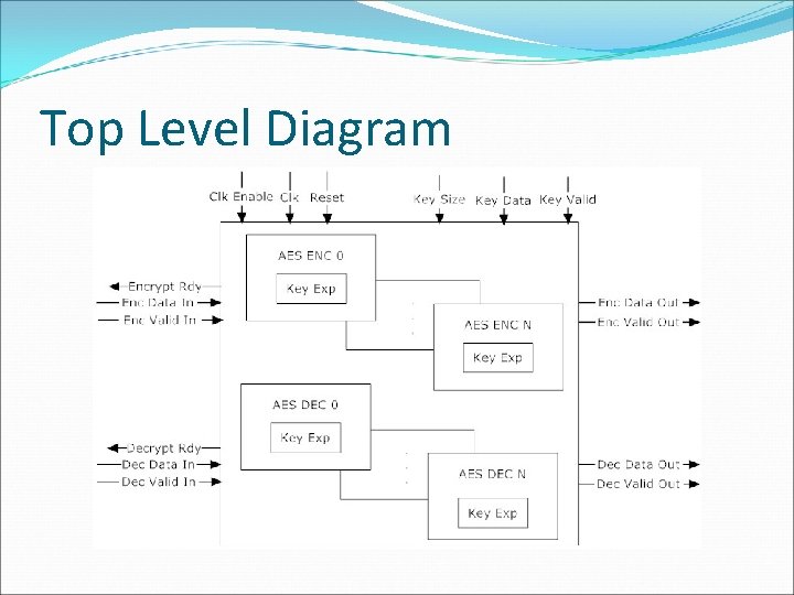
Objectives Design an FPGA that is capable of AES encryption and decryption with 128, 192, and 256 bit keys. Optimize encryption/decryption throughput by implementing multiple cores Synthesize multi-core design and generate a simulated throughput
AES Core Modules Used AES Core Modules developed by Jerzy Gbur Contains: key_expansion. vhd – 128, 192, or 256 bit key expansion module aes_enc. vhd – AES encryption module aes_dec. vhd – AES decryption module
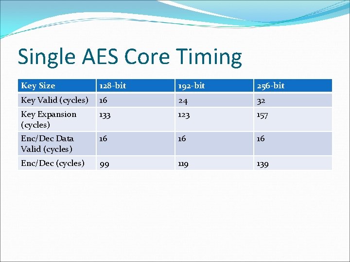
Single AES Core Timing Key Size 128 -bit 192 -bit 256 -bit Key Valid (cycles) 16 24 32 Key Expansion (cycles) 133 123 157 Enc/Dec Data Valid (cycles) 16 16 16 Enc/Dec (cycles) 99 119 139
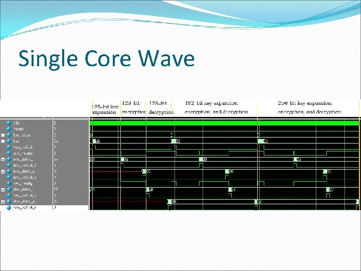
Single Core Wave
Top Level Diagram
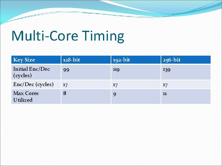
Multi-Core Timing Key Size 128 -bit 192 -bit 256 -bit Initial Enc/Dec (cycles) 99 119 139 Enc/Dec (cycles) 17 17 17 Max Cores Utilized 8 9 11
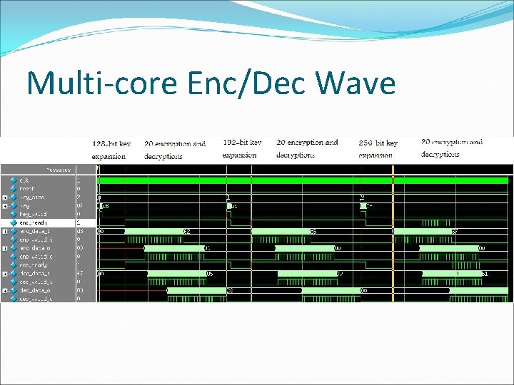
Multi-core Enc/Dec Wave
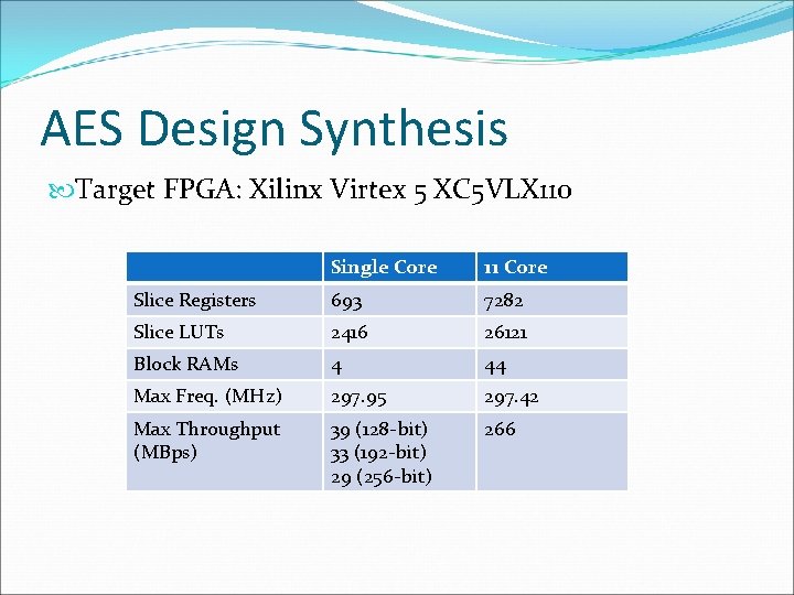
AES Design Synthesis Target FPGA: Xilinx Virtex 5 XC 5 VLX 110 Single Core 11 Core Slice Registers 693 7282 Slice LUTs 2416 26121 Block RAMs 4 44 Max Freq. (MHz) 297. 95 297. 42 Max Throughput (MBps) 39 (128 -bit) 33 (192 -bit) 29 (256 -bit) 266
Growth Opportunities Add more Enc/Dec inputs and 11 -core modules Optimize the design for size Allow the key to be different for each core Use different AES Core
Questions Design is located at: http: //code. google. com/p/multicore-aes-fpga/ If you have any questions please email me at: wdwhiteh@iastate. edu
- Slides: 11