FPGA Design Techniques 2003 Xilinx Inc All Rights

- Slides: 32

FPGA Design Techniques © 2003 Xilinx, Inc. All Rights Reserved

Objectives After completing this module, you will be able to: • • Increase design performance by duplicating flip-flops Increase design performance by adding pipeline stages Increase board performance by using I/O flip-flops Build reliable synchronization circuits FPGA Design Techniques - 5 - 3 © 2003 Xilinx, Inc. All Rights Reserved For Academic Use Only

Outline • • • FPGA Design Techniques - 5 - 4 Duplicating Flip-flops Pipelining I/O Flip-Flops Synchronization Circuits Summary © 2003 Xilinx, Inc. All Rights Reserved For Academic Use Only

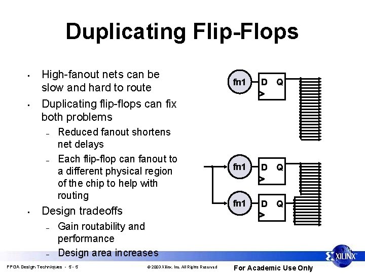
Duplicating Flip-Flops • • High-fanout nets can be slow and hard to route Duplicating flip-flops can fix both problems – – • Reduced fanout shortens net delays Each flip-flop can fanout to a different physical region of the chip to help with routing Design tradeoffs – – fn 1 D Q Gain routability and performance Design area increases FPGA Design Techniques - 5 © 2003 Xilinx, Inc. All Rights Reserved For Academic Use Only

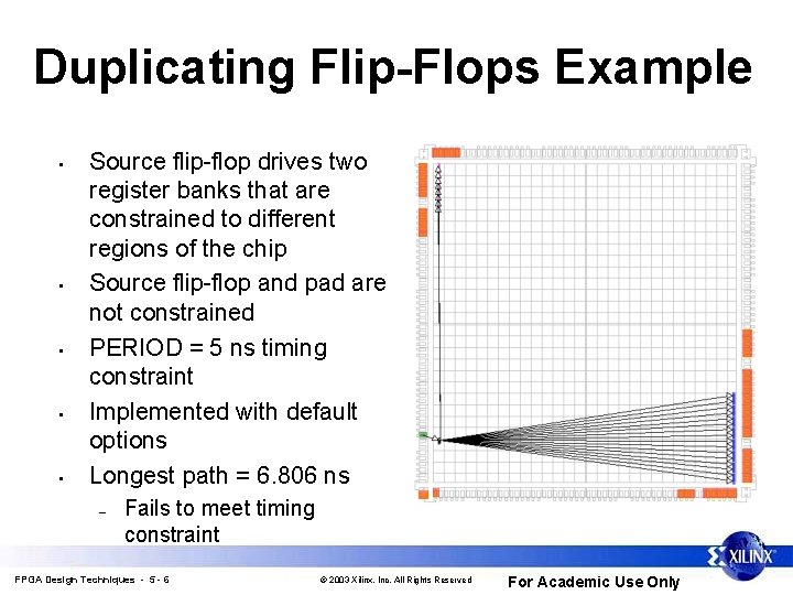
Duplicating Flip-Flops Example • • • Source flip-flop drives two register banks that are constrained to different regions of the chip Source flip-flop and pad are not constrained PERIOD = 5 ns timing constraint Implemented with default options Longest path = 6. 806 ns – Fails to meet timing constraint FPGA Design Techniques - 5 - 6 © 2003 Xilinx, Inc. All Rights Reserved For Academic Use Only

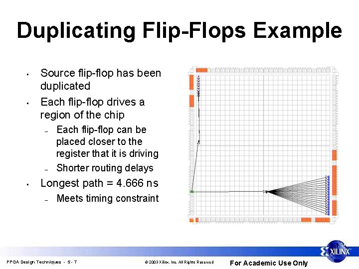
Duplicating Flip-Flops Example • • Source flip-flop has been duplicated Each flip-flop drives a region of the chip – – • Each flip-flop can be placed closer to the register that it is driving Shorter routing delays Longest path = 4. 666 ns – Meets timing constraint FPGA Design Techniques - 5 - 7 © 2003 Xilinx, Inc. All Rights Reserved For Academic Use Only

Tips on Duplicating Flip-Flops • Name duplicated flip-flops _a, _b: NOT _1, _2 – – Numbered flip-flops are mapped into the same slice by default You, generally, want duplicated flip-flops to be separated • • Explicitly create duplicate flip-flops in your HDL code – Most synthesis tools have automatic fanout-control features • • – However, they do not always pick the best division of loads Also, duplicated flip-flops will be named _1, _2 Many synthesis tools will optimize-out duplicated flip-flops • • Especially if the loads are spread across the chip Tell your synthesis tool to keep redundant logic Do not duplicate flip-flops that are sourced by asynchronous signals – – Synchronize the signal first Feed the synchronized signal to multiple flip-flops FPGA Design Techniques - 5 - 8 © 2003 Xilinx, Inc. All Rights Reserved For Academic Use Only

Outline • • • FPGA Design Techniques - 5 - 9 Duplicating Flip-Flops Pipelining I/O Flip-Flops Synchronization Circuits Summary © 2003 Xilinx, Inc. All Rights Reserved For Academic Use Only

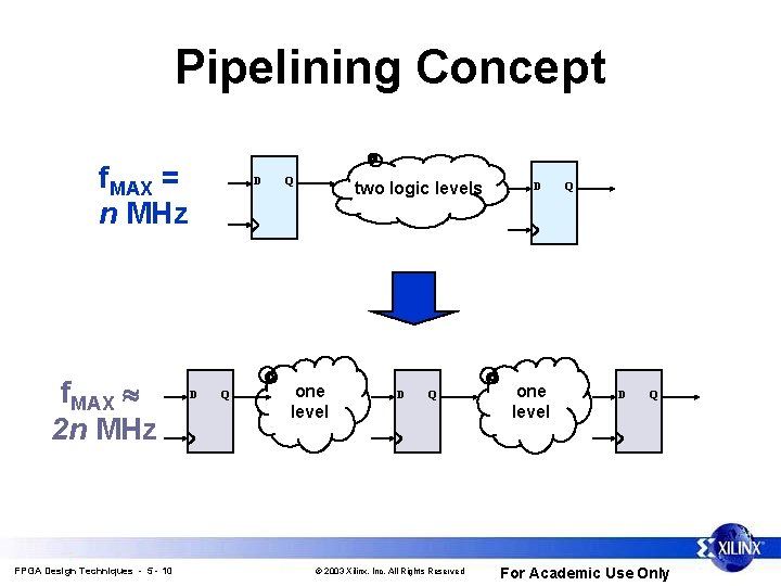
Pipelining Concept f. MAX = n MHz f. MAX 2 n MHz FPGA Design Techniques - 5 - 10 D D Q Q two logic levels one level D Q © 2003 Xilinx, Inc. All Rights Reserved D one level Q D Q For Academic Use Only

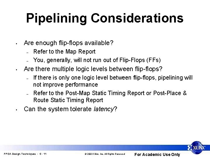
Pipelining Considerations • Are enough flip-flops available? – – • Are there multiple logic levels between flip-flops? – – • Refer to the Map Report You, generally, will not run out of Flip-Flops (FFs) If there is only one logic level between flip-flops, pipelining will not improve performance Refer to the Post-Map Static Timing Report or Post-Place & Route Static Timing Report Can the system tolerate latency? FPGA Design Techniques - 5 - 11 © 2003 Xilinx, Inc. All Rights Reserved For Academic Use Only

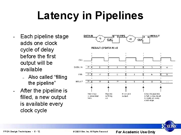
Latency in Pipelines • Each pipeline stage adds one clock cycle of delay before the first output will be available – • Also called “filling the pipeline” After the pipeline is filled, a new output is available every clock cycle FPGA Design Techniques - 5 - 12 © 2003 Xilinx, Inc. All Rights Reserved For Academic Use Only

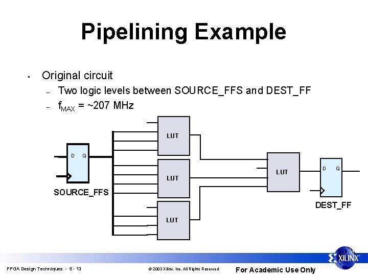
Pipelining Example • Original circuit – – Two logic levels between SOURCE_FFS and DEST_FF f. MAX = ~207 MHz LUT D Q LUT D LUT Q SOURCE_FFS DEST_FF LUT FPGA Design Techniques - 5 - 13 © 2003 Xilinx, Inc. All Rights Reserved For Academic Use Only

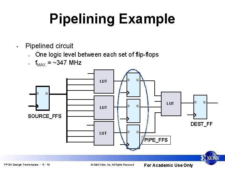
Pipelining Example • Pipelined circuit – – One logic level between each set of flip-flops f. MAX = ~347 MHz D LUT D Q Q D LUT Q SOURCE_FFS DEST_FF LUT D Q PIPE_FFS FPGA Design Techniques - 5 - 14 © 2003 Xilinx, Inc. All Rights Reserved For Academic Use Only

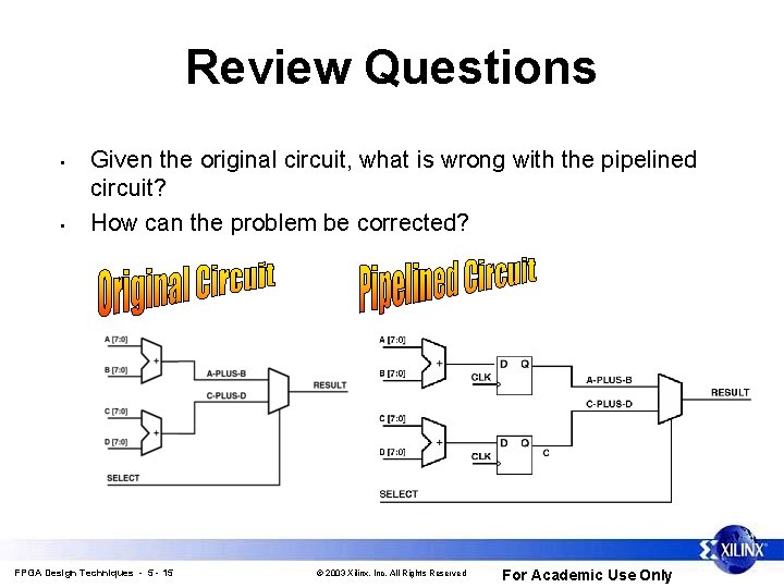
Review Questions • • Given the original circuit, what is wrong with the pipelined circuit? How can the problem be corrected? FPGA Design Techniques - 5 - 15 © 2003 Xilinx, Inc. All Rights Reserved For Academic Use Only

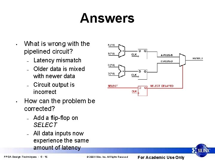
Answers • What is wrong with the pipelined circuit? – – – • Latency mismatch Older data is mixed with newer data Circuit output is incorrect How can the problem be corrected? – – Add a flip-flop on SELECT All data inputs now experience the same amount of latency FPGA Design Techniques - 5 - 16 © 2003 Xilinx, Inc. All Rights Reserved For Academic Use Only

Outline • • • FPGA Design Techniques - 5 - 17 Duplicating Flip-Flops Pipelining I/O Flip-Flops Synchronization Circuits Summary © 2003 Xilinx, Inc. All Rights Reserved For Academic Use Only

I/O Flip-Flop Overview • Each Virtex™-II I/O block contains six flip-flops – – • INFF on the input, OFF on the output, ENFF on the 3 state enable* Single-data-rate or double-data-rate support I/O flip-flops provide guaranteed setup, hold, and clock -to-out times when the clock signal comes from a BUFG FPGA Design Techniques - 5 - 18 © 2003 Xilinx, Inc. All Rights Reserved For Academic Use Only

Accessing I/O Flip-Flops • During synthesis – – • Timing-driven synthesis can force flip-flops into IOBs Some tools support attributes or synthesis directives to mark flip-flops for placement in an IOB Xilinx Constraint Editor – Select the Misc tab, then specify registers that should be placed into IOBs • • During the Map phase of implementation – – • Need to know the instance name of each register Map Properties, Pack I/O Registers/Latches into IOBs is on by default Timing-driven packing will also move registers into IOBs for critical paths Check the Map Report to confirm that IOB flip-flops have FPGA Design Techniques - 5 - 19 © 2003 Xilinx, Inc. All Rights Reserved For Academic Use Only

Outline • • • FPGA Design Techniques - 5 - 20 Duplicating Flip-Flops Pipelining I/O Flip-Flops Synchronization Circuits Summary © 2003 Xilinx, Inc. All Rights Reserved For Academic Use Only

Synchronization Circuits • What is a synchronization circuit? – • Why do I need synchronization circuits? – – • Captures an asynchronous input signal and outputs it on a clock edge Prevent setup and hold time violations End result is a more reliable design When do I need synchronization circuits? – Signals cross between unrelated clock domains • – Between related clock domains, relative PERIOD constraints are sufficient Chip inputs that are asynchronous FPGA Design Techniques - 5 - 21 © 2003 Xilinx, Inc. All Rights Reserved For Academic Use Only

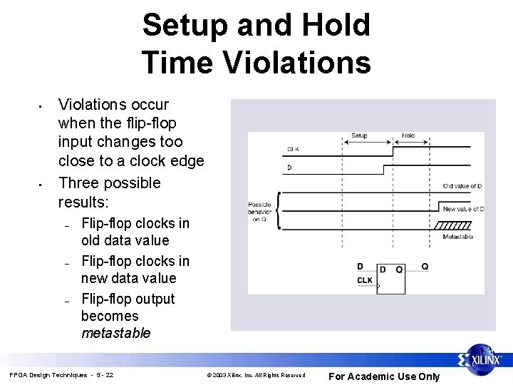
Setup and Hold Time Violations • • Violations occur when the flip-flop input changes too close to a clock edge Three possible results: – – – Flip-flop clocks in old data value Flip-flop clocks in new data value Flip-flop output becomes metastable FPGA Design Techniques - 5 - 22 © 2003 Xilinx, Inc. All Rights Reserved For Academic Use Only

Metastability • Flip-flop output enters a transitory state – Neither a valid 0 nor a valid 1 • – • • Remains in this state for an unpredictable length of time before settling to a valid 0 or 1 Due to its statistical nature, the occurrence of metastable events can only be reduced, not eliminated Mean Time Between Failures (MTBF) is exponentially related to the length of time the flip-flop is given to recover – • May be interpreted as 0 by some loads and as 1 by others A few extra ns of recovery time can dramatically reduce the chances of a metastable event The circuits shown in this section allow a full clock cycle for metastable recovery FPGA Design Techniques - 5 - 23 © 2003 Xilinx, Inc. All Rights Reserved For Academic Use Only

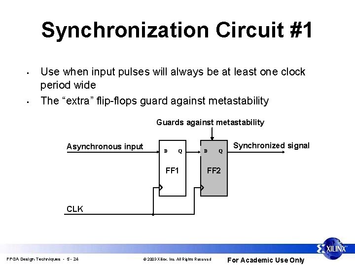
Synchronization Circuit #1 • • Use when input pulses will always be at least one clock period wide The “extra” flip-flops guard against metastability Guards against metastability Asynchronous input D Q FF 1 D Q Synchronized signal FF 2 CLK FPGA Design Techniques - 5 - 24 © 2003 Xilinx, Inc. All Rights Reserved For Academic Use Only

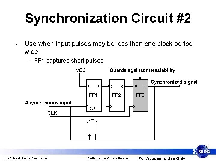
Synchronization Circuit #2 • Use when input pulses may be less than one clock period wide – FF 1 captures short pulses VCC Guards against metastability D Q FF 1 D Q FF 2 D Q Synchronized signal FF 3 Asynchronous input CLR CLK FPGA Design Techniques - 5 - 25 © 2003 Xilinx, Inc. All Rights Reserved For Academic Use Only

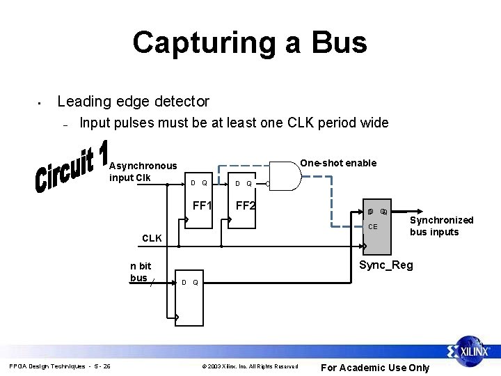
Capturing a Bus • Leading edge detector – Input pulses must be at least one CLK period wide Asynchronous input Clk One-shot enable D Q FF 1 FF 2 D Q CE CLK n bit bus FPGA Design Techniques - 5 - 26 Synchronized bus inputs Sync_Reg DD Q Q © 2003 Xilinx, Inc. All Rights Reserved For Academic Use Only

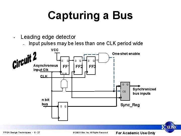
Capturing a Bus • Leading edge detector – Input pulses may be less than one CLK period wide VCC One-shot enable D Asynchronous Input Clk CLK Q FF 1 D Q FF 2 D Q FF 3 CLR D Q CE n bit bus FPGA Design Techniques - 5 - 27 Synchronized bus inputs Sync_Reg D Q © 2003 Xilinx, Inc. All Rights Reserved For Academic Use Only

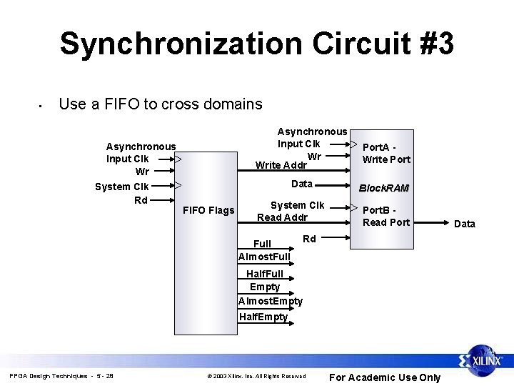
Synchronization Circuit #3 • Use a FIFO to cross domains Asynchronous Input Clk Wr System Clk Rd FIFO Flags Asynchronous Input Clk Wr Write Addr Port. A Write Port Data Block. RAM System Clk Read Addr Full Almost. Full Port. B Read Port Rd Half. Full Empty Almost. Empty Half. Empty FPGA Design Techniques - 5 - 28 © 2003 Xilinx, Inc. All Rights Reserved For Academic Use Only Data

Outline • • • FPGA Design Techniques - 5 - 29 Duplicating Flip-Flops Pipelining I/O Flip-Flops Synchronization Circuits Summary © 2003 Xilinx, Inc. All Rights Reserved For Academic Use Only

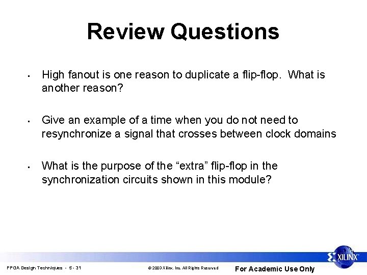
Review Questions • • • High fanout is one reason to duplicate a flip-flop. What is another reason? Give an example of a time when you do not need to resynchronize a signal that crosses between clock domains What is the purpose of the “extra” flip-flop in the synchronization circuits shown in this module? FPGA Design Techniques - 5 - 31 © 2003 Xilinx, Inc. All Rights Reserved For Academic Use Only

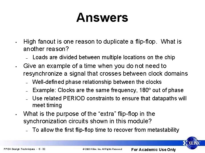
Answers • High fanout is one reason to duplicate a flip-flop. What is another reason? – • Give an example of a time when you do not need to resynchronize a signal that crosses between clock domains – – – • Loads are divided between multiple locations on the chip Well-defined phase relationship between the clocks Example: Clocks are the same frequency, 180º out of phase Use related PERIOD constraints to ensure that datapaths will meet timing What is the purpose of the “extra” flip-flop in the synchronization circuits shown in this module? – To allow the first flip-flop time to recover from metastability FPGA Design Techniques - 5 - 32 © 2003 Xilinx, Inc. All Rights Reserved For Academic Use Only

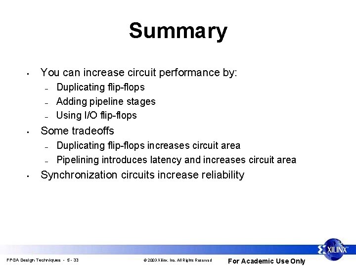
Summary • You can increase circuit performance by: – – – • Some tradeoffs – – • Duplicating flip-flops Adding pipeline stages Using I/O flip-flops Duplicating flip-flops increases circuit area Pipelining introduces latency and increases circuit area Synchronization circuits increase reliability FPGA Design Techniques - 5 - 33 © 2003 Xilinx, Inc. All Rights Reserved For Academic Use Only

Where Can I Learn More? • Data Book: http: //support. xilinx. com Documentation Databook – – • Switching Characteristics Detailed Functional Description Input/Output Blocks (IOBs) Application Notes: http: //support. xilinx. com Documentation App Notes – – XAPP 094: Metastability Recovery XAPP 225: Data to Clock Phase Alignment FPGA Design Techniques - 5 - 34 © 2003 Xilinx, Inc. All Rights Reserved For Academic Use Only