FPGA Based Trigger System for the Klystron Department

FPGA Based Trigger System for the Klystron Department By Darius Gray

What is the problem? ? • Much of the technology used in the Klystron Department is out dated. About 60’s and 70’s technology. • LCLS requirements are 50 f. S rms jitter on the output of a 5045 klystron. Existing systems do not allow measurements of this stability. • A trigger system upgrade is the first step in meeting this requirement.

Old Equipment

Trigger System Upgrade • Upgrades can be implemented to increase the capabilities of the test station. • The trigger system upgrade will allow precision timing for klystron related triggers – Beam Pulse Trigger – RF Trigger – Data Collection Triggers

SLAC 5045 Klystron 60 MW RF Output 500 W RF Input 100 MW Beam Power 5 u. S Pulse width

Klystron Test Stand

• The objective of the research is to develop the trigger system using Field Programmable Gate Array (FPGA) technology with a user interface that will allow one to communicate with the FPGA via a Universal Serial Bus (USB).

• My mentor, Ron Akre, designed the test stand trigger system that would meet the needs of the test lab.

• My primary focus of this task is to program the FPGA.

The FPGA is the black chip in the center of the PCB Board.
 the central timing system")
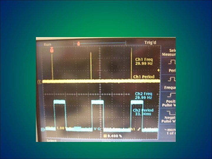
• This design consisted of two parts: • 1) the central timing system and – Generates 1 Hz, 360 Hz, and 119 MHz • 2) the FPGA based trigger generator. – Uses 1 Hz, 360 Hz, and 119 MHz to generate triggers.

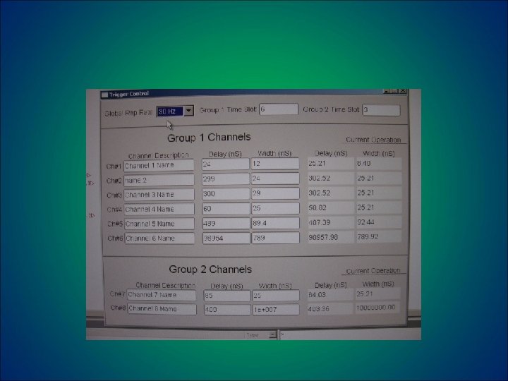
• The operator sets the value for the delay, width, rate, and, if applicable, the phase shift value of the trigger in a user interface.

• The FPGA based trigger generator takes in a signal and generates eight independent triggers.
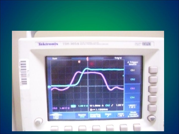

Non DLL channel with 80 ps of jitter.

The Rep rate is 180 Hz using the DLL and there is 172 ps of jitter in two different states.

Questions? ?
- Slides: 19